Abstract— This work presents a combined magnetometer / accelerometer sharing a single surface micromachined structure. The device utilizes electrical current switching between two perpendicular directions on the structure to achieve a 2D in-plane magnetic field measurement based on the Lorentz force. The device can concurrently serve as a 1D accelerometer for out-of-plane acceleration, when the current is switched off. Accordingly, the proposed design is capable of separating magnetic and inertial force measurements, achieving higher accuracy through a single compact device. The sensor supports static operation at atmospheric pressure, precluding the need for complex vacuum packaging. It can alternatively operate at resonance under vacuum for enhanced sensitivity. The device is fabricated using a low temperature surface micromachining technology, which is fully adapted for above-IC integration on standard CMOS substrates. The resonance frequency of one of the fabricated structures is measured to be 6.53 kHz, with a quality factor of ~30, at a10 mTorrambient vacuum level. The magnetic field and acceleration sensitivities of the device are measured using discrete electronics to be 1.57 pF/T and 1.02 fF/g, respectively, under static operation.
Index Terms—Microelectromechanical systems (MEMS), Lorentz force magnetometers, micromachined accelerometers, silicon carbide (SiC), surface micromachining, above-IC integration.
I. INTRODUCTION
Micromachined Lorentz force magnetometers are receiving considerable attention in the sensing community, as they can be fabricated without requiring any custom magnetic
Manuscript received June 3, 2014; revised September 9, 2014. This work was supported in part by McGill University, in part by the Natural Sciences and Engineering Research Council of Canada, in part by the Quebec Fund for Research in Nature and Technology (FQRNT), and in part by the Microsystems Strategic Alliance of Quebec (ReSMiQ).
M. Y. Elsayed and P.-V. Cicek are with the McGill Wireless Integrated Circuits and Microelectromechanical Systems (WICs & MEMS) Group, McGill University, Montreal, QC, H3A 0E9, Canada (emails: [email protected] and [email protected]).
F. Nabki is with the CoFaMic Research Center, Université du Québec à Montréal (UQAM), Montreal, QC, H3C 3P8, Canada (e-mail: [email protected]).
M. N. El-Gamal is with the Department of Electrical and Computer Engineering, McGill University, Montreal, QC, H3A 0E9, Canada (email: [email protected]).
materials (e.g., integrated permanent magnets in [1]). This allows for their co-fabrication alongside other MEMS sensors on the same chip, for augmented functionality with minimum impact on form factor. Such integration is highly attractive for consumer electronics applications, where MEMS sensors are playing an increasing role each day. In such cost-sensitive applications, exotic magnetic materials often do not justify the added costs and fabrication complexity, and limit the compatibility of magnetometers with other MEMS sensing structures and integrated circuits (ICs). In [2], an out-of-plane Lorentz force magnetometer and a ferromagnetic in-plane nickel magnetometer are presented, requiring high temperature fabrication steps (e.g., 800◦C), while, in [3-4], a Lorentz force-based resonant sensor for in-plane or out-of-plane magnetic fields is built using SOI technology. While two similar orthogonal structures could be used for 3D sensing, these devices are not suitable for post-CMOS monolithic integration. In [5], a co-fabricated CMOS-MEMS magnetometer is presented in a TSMC 0.35 µm technology, but is restricted to the materials and constraints inherent to that semiconductor process node.
Alternatively, sensors that are amenable to above-IC integration present lower parasitics to the associated readout circuitry, resulting in an improved overall sensitivity. Furthermore, the area sharing made possible by overlaying the sensors with the electronics allows for smaller overall chip size, compared to the side-by-side co-fabrication approach. Accordingly, this work presents a Lorentz force based magnetometer / accelerometer combined sensor, made from a low temperature, above-IC-compatible fabrication process. The proposed sensor relies on switching an electrical current between two perpendicular directions on the device structure to achieve a 2D in-plane magnetic field measurement. Concurrently, the device serves as a 1D accelerometer for out-of-plane acceleration, by switching the current off and by monitoring the structure's capacitive change in response to acceleration. The design can thus separate magnetic and inertial force measurements, utilizing a single compact device. The proposed sensor supports static operation at atmospheric pressure to avoid the need for complex vacuum packaging. Alternatively, it is also capable of operating at resonance under vacuum for enhanced sensitivity. The device is fabricated using a silicon carbide (SiC) surface micromachining technology as in [6-8], which is fully adapted for above-IC integration on standard CMOS substrates.
Surface Micromachined Combined
Magnetometer / Accelerometer
for Above-IC Integration
Mohannad Y. Elsayed, Student Member, IEEE, Paul-Vahé Cicek, Student Member, IEEE,
Frederic Nabki, Member, IEEE, and Mourad N. El-Gamal, Member, IEEE
500 μm 500 μm 250 μm 250 μm 9 μm 10 μm 40 μm Proof
mass Release holes
Top electrode pad Bottom
electrode pad
Fig. 1. SEM micrograph of a fabricated device.
Top View Cross-Section
i
Vertical motion due to
By + Az
i
Vertical motion due to
Bx + Az By Bx Bottom electrode Top electrode Phase 1 Phase 2
Fig. 2. First two phases of the sensing cycle showing the current direction together with a side cross-section view illustrating the device displacement. This paper first describes the device design, and then
presents finite-elements simulation results. The process flow for the fabrication technology is then detailed, and measurement results are presented and discussed.
II. DESIGN
The principle of operation for a Lorentz force magnetometer can be explained as follows. If a magnetic field B is acting on a wire of length l and carrying a current I, the wire will be affected by a Lorentz force (FLorentz) orthogonal to both the wire and the magnetic field. This force is given by
) (l B i
FLorentz = × . (1) As such, by measuring the displacement caused by the force, while knowing the current and length, the magnetic field can be inferred.
An SEM micrograph of the fabricated device is shown in Fig. 1. Bowing is apparent in the device due to its relatively large area, and the residual stresses present in the film stack. The sensor is composed of: i) a 2 µm-thick 500 μm-wide square suspended SiC structure acting as the current carrying element for magnetometer operation and concurrently serving as the proof mass for the accelerometer; ii) four 250 μm-long and 9 μm-wide suspension beams, anchored from their ends, holding the proof mass and allowing for its free motion; iii) a sensing electrode underneath the structure used for the capacitive detection of the out-of-plane motion resulting from Lorentz or inertial forces; and iv) a metallic layer underlying the SiC structure in order to serve as a low resistivity path for the current, thus helping to reduce electrical noise.
The beam dimensions are chosen to adjust the stiffness of the supports in order to provide adequate sensitivity and ensure the structural integrity of the device. The spring constant k of a simple cantilever beam is given by [9]
3 3 4 simple beam wt k E l = , (2)
where E is the Young’s Modulus of the beam material (amorphous SiC in this case), w is the beam width, t is the structure thickness, and l is the beam length. A summary of the device design parameters is given in Table I.
During device operation, the sensing cycle is divided into three successive phases, as illustrated in Fig. 2:
1) The current is driven along the x-axis, from left to right, causing the resulting Lorentz force to induce a displacement along the z-axis, due to any magnetic field in the y-axis. This displacement is detected capacitively by the sense electrode, and can be used to infer the y-axis component of the magnetic field.
2) The current is directed along the y-axis, from bottom to top.
The resulting Lorentz force then causes a displacement along the z-axis, due to any magnetic field along the x-axis. Capacitive detection at the sense electrode is used to determine the x-axis component of the magnetic field. Notably, measurements in phases 1 and 2 are sensitive to external z-axis inertial force.
3) The current is switched off so that the motion due to the z-axis inertial force is detected and used to cancel out its effect on the magnetic field measurements in phases 1 and 2, achieving a high accuracy combined 2D magnetometer / 1D accelerometer.
In order to increase the number of operation axes of the device, lateral electrodes could eventually be added at the perimeter of the proof mass as suggested in [10] to enable in-plane motion detection and achieve a 3D magnetometer / 3D accelerometer.
TABLE I
SUMMARY OF DEVICE DESIGN PARAMETERS
Parameter Value Proof mass 500 μm × 500 μm Structure thickness 2 μm Suspension dimensions 250 μm × 9 μm Capacitive gap 0.5 μm Spring constant (keq) 1.07 N/m Resonance frequency 4.03 kHz
Fig. 4. First derivative of the total force (dFtotal/dz) vs the displacement (z) for
different values of the inter-electrode gap (d). The selected inter-electrode gap is underlined and the resulting maximum displacement (zmax.) is shown.
Fig. 3. Forces affecting the structure versus vertical displacement. III. CASIMIR FORCE
The Casimir force is an attractive force that acts between two close parallel uncharged conducting plates. It is due to quantum vacuum fluctuations of the electromagnetic field. As the device presented here has a large electrode area and a relatively small gap, this force must be considered. In addition to the Casimir force, the suspended top plate of the device is affected by several other forces, namely the gravitational force, the applied Lorentz and inertial forces, and the suspension spring forces such that
total Casimir gravitational Lorentz inertial spring
F =F +F +F +F +F . (3)
The Casimir force is proportional to the electrode area and is inversely proportional to the fourth power of the distance between the two electrodes. It is given by [4]
480 PM PM Casimir 4 πhcw L F (d z) = − , (4)
where h is Planck’s constant, c is the speed of light in vacuum, wPM is the width of the proof mass (top electrode), and LPM is its length, d is the nominal capacitive gap between the electrodes, and z is the displacement of the top electrode. The force related to the weight of the structure is given by
gravitational SiC PM PM
F =
ρ
gw L t, (5)where ρSiC is the density of the SiC structural material, and g is Earth’s gravitational acceleration. The balancing spring force is given by
spring eq
F = −k z. (6)
where keq is the equivalent spring constant of the structure. At equilibrium, the resultant force must be zero (i.e., Ftotal = 0), as illustrated in Fig. 3, where all the forces are plotted along with that of the restorative spring force. Furthermore, a necessary condition is that the first derivative of total force (i.e., dFtotal/dz) be negative at the point of equilibrium, such that
. 5 0 120 total PM PM eq dF πhcw L k dz = (d−z) − < . (7) Figure 4 shows dFtotal/dz for different values of the gap between the electrodes (d). For small values of d, dFtotal/dz is always positive for all positive displacement (z) values. This means that the top electrode would always be pulled-in by the Casimir force directly after release such that there is no stable
equilibrium state. As d increases beyond a certain value, dcritical, a stable equilibrium range, where the derivative is negative for positive z, is reached. This equilibrium ensures that the structure will not collapse as a result of Casimir force after release. In order to calculate dcritical, the Casimir force for small values of z can be neglected as it is very small, and will otherwise complicate the solution due to its 1/(d-z)4
dependence. For a critically stable condition without pull-in after release, the spring force should balance the weight, such that
eq PI SiC PM PM
k z =
ρ
gw L t, (8)where zPI is the displacement in this critically stable situation. By combining (7) and (8), dcritical can be calculated using
5 120 SiC PM PM PM PM critical eq gw L t πhcw L d d k k ρ > = + . (9)
Using (9), the value for dcritical is calculated to be of 275 nm. The maximum possible displacement of the structure before pull-in collapse due to the Casimir force is expressed as
5 max 120 PM PM πhcw L z d k = − . (10)
Accordingly, a sacrificial layer thickness (gap between the electrodes) of 500 nm is selected in order to ensure structural integrity of the device after release, and to allow sufficient displacement before a pull-in collapse occurs. The derivative of the total force vs the displacement for this selected gap size is shown in Fig. 4, yielding a stable equilibrium region for displacements below 239 nm. This allowable displacement range allows for a good dynamic range of the device.
Note that at all times the electrical potential difference between the electrodes must be kept well below the electrostatic pull-in voltage given by [9]
3 0 8 27 eq PI PM PM k d V L w ε = , (11)
where ε0 is the free space permittivity. The pull-in voltage value is calculated from (11) to be ~130 mV. Accordingly, careful attention needs to be given to this issue during the sensing circuit design, in order to avoid electrostatic pull-in and collapsing of the structure, as will be discussed in section VI. Notably, this calculated pull-in value is expected to be
Fig. 5. FEM simulation showing the structure displacement as a result of a force along the z-axis.
below the actual value, because of the bowing observed in Fig. 1.
IV. SIMULATION RESULTS
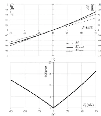
A finite-element simulation illustrating the displacement of the structure as a result of a force along the z-axis is shown in Fig. 5. Figure 6(a) shows simulation results for the displacement Δd relative to Fz, the external force applied along the z-axis. In order to calculate ΔCactual, the resulting change in capacitance for the device, a parallel plate capacitor approximation is used and fringing fields are neglected:
, (12) where A is the area of the capacitor plate and d is the nominal gap size, defined by the thickness of the sacrificial polyimide.
From Taylor series expansion, a linear approximation for the change in capacitance can be made for Δd<<d such that
. (13) Figure 6(a) shows the sensor response calculated using (12) as well as the linear approximation given in (13). Accordingly, the spring constant keq. of the structure can be calculated to be of 1.07N/m, which corresponds to a capacitance sensitivity of 8.24 μF/N. This translates to a magnetic field sensitivity of 8.24 nF/A/T for a structure length of 1 mm in which current flows to generate the Lorentz force, as deduced from (1), and an acceleration sensitivity of 121 fF/g, stemming from (5). The percentage error between the actual and linear capacitance changes is shown in Fig. 6(b), and is expressed as
. (14)
The actual change in capacitance coincides well with the linear approximation for small displacements, but starts to differ for larger motion. By limiting the worst-case linearity error to 10%, the dynamic range of the device is found to be ±50 nN. This value corresponds either to a detected magnetic field of ±50 mT with a driving current of 1 mA, or to a detected acceleration of ±3.4 g.
Furthermore, in order to determine the maximum shock the device can survive before collapsing, a step input acceleration is considered. The damping ratio (ζ) is calculated to be ~0.0167 from the measured value of the quality factor
(Q), given in section VI. Therefore, as shown in [12], the system’s step response experiences an overshoot percentage (Mp) of 95%, according to
. (15)
By limiting the maximum displacement overshoot to 239 nm (zmax. before Casimir pull-in, calculated in section III), determining the displacement step input yielded by the overshoot percentage, and calculating the required acceleration to generate this step, the maximum shock the device can survive is calculated to be ±9 g.
V. FABRICATION PROCESS
The fabrication process sequence is illustrated in Fig. 7. A silicon substrate covered with a layer of thermal oxide is used for this prototype. The process is designed to be fully compatible with monolithic integration on standard CMOS substrates. First, a 200 nm layer of aluminum is deposited onto the substrate by DC sputtering. The aluminum is then patterned and wet etched using phosphoric-acetic-nitric acid (PAN) etchant to form the bottom electrode and the pads, as shown in Fig. 7(a). A 0.5 µm sacrificial polyimide layer is then spin coated. Then, the polymer is oven cured at 200°C to form the vertical gaps for the sense capacitor. An oxygen reactive ion etch patterns the polyimide to allow for the eventual anchoring of the structural supports to the substrate, as shown in Fig. 7(b). Afterwards, the structural stack is deposited, including the following layers, ordered from top to bottom: i) A 2 µm amorphous SiC layer, which is the main structural layer; ii) a 200 nm aluminum layer to form the low resistance path for the current, reducing the electrical noise; and iii) a 20 nm layer of chromium acting as an etch stop layer
(a)
(b)
Fig. 6. (a) Change in capacitance (linear approximation, actual) and displacement vs. external force applied, and (b) percentage error of
Fig. 7. Simplified device fabrication process flow.
Fig. 9. Measured resonance characteristics of fabricated devices (10 mTorr vacuum).
Fig. 10. Schematic of the test setup used for the magnetic characterization of the device.
Fig. 8. Simplified schematic of the test setup used for resonance characterization.
during the second aluminum etch.
The stack is covered by a 600 nm chromium layer to act as a hard mask while etching the SiC layer. The deposition of the four layers is performed using DC sputtering, after which the chromium hard mask is patterned and wet etched. The SiC is then dry etched using nitrogen trifluoride (NF3) reactive ion
etching, stopping onto the underlying aluminum layer. Subsequently, the chromium hard mask is wet stripped as shown in Fig. 7(c), and the underlying aluminum and chromium layers are patterned using wet etching, as shown in Fig. 7(d). During this step, the chromium layer acts as an etch stop, protecting the exposed regions of the first aluminum layer from the etch of the second aluminum layer. Finally, the process is completed by dry release of the sacrificial polyimide using oxygen plasma, as shown in Fig. 7(e). A dry release mitigates the risk of stiction, compared to the more common wet release methods. Release holes with 10 μm diameter and 40 μm spacing are incorporated within the suspended structure to facilitate the release process.
VI. MEASUREMENT RESULTS A. Resonance Characteristics
The resonance characteristics of the fabricated devices are measured under vacuum using the test setup shown in Fig. 8. Bias tees are used to decouple the high frequency
measurement signals from the DC signals, and apply the DC voltages to the device, which are necessary for electrostatic actuation. Measurement results for devices with 200 μm support beam length are shown in Fig. 9. They exhibit a resonance frequency (fr) of 6.53kHz and a quality factor (Q) of 30 under 10 mTorr vacuum level. This Q value is calculated based on the 3-dB bandwidth inferred in Fig. 9. Note that the actual measured peak is slightly lower than 3-dB. However, this method is used to ascertain a worst case value. Alternatively, considering the resonance curve as symmetric and calculating the bandwidth using the right side of the curve only, a Q of 125 is obtained. Finite-element Eigen frequency simulation indicates a resonance frequency of 4.03 kHz. The difference between the simulated and measured values can most likely be attributed to the residual stress also at play in the bowing of the structure.
B. Magnetic Field Response
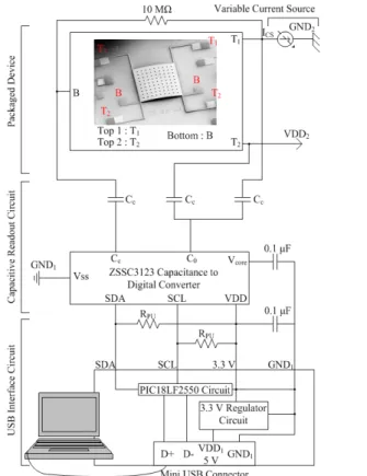
The magnetic field response of the fabricated devices was characterized using a variable electromagnet and discrete electronics. The schematic of the test setup used is shown in
Fig. 10, where DC current is generated by a variable current source and flows through the top structure of the device from pad T1 to pad T2. This current serves to generate a Lorentz
force when the device is subjected to an in-plane magnetic field normal to the current. The resulting capacitance change between the top (T) and bottom (B) electrodes of the device is monitored and used to acquire the magnetic field. The ZMDI ZSSZ3123 capacitance to digital converter chip [13] is configured to measure the capacitance of the device relative to an internal reference capacitor. This chip outputs a 1 MHz 1.8 V square wave excitation signal for the capacitance measurement. As the bowing that the fabricated structure exhibited has widened the gap to ~5 μm, the corresponding electrostatic pull-in voltage has increased to 4.23 V. Accordingly, electrostatic pull-in will not occur during sensing. Coupling capacitors (Cc) of 22 μF are used to couple the AC signal between the device and the capacitance readout chip, as well as prevent any DC current leakage from the current source circuit to the chip. A large resistor of 10 MΩ is connected between the top and bottom electrodes of the device to make sure that they stay at the same DC potential in order to avoid any electrostatic force between them. The capacitance readout chip communicates the digital words for the measured capacitance through an I2C interface to the USB interface
circuit using the two pull-up resistors RPU (2.2 kΩ). A Microchip PIC18LF2550 microcontroller [14] serves to accept the digital data from the capacitance readout circuit through the I2C interface and then transmits it to the host PC via USB.
The microcontroller is also used for configuration of the capacitance readout chip.
The schematic of the current source circuit is shown in Fig. 11, utilizing the Analog Devices MAT14 matched monolithic quad transistor chip [15]. One transistor is connected in a diode configuration with two resistors (Rlimit and Rtune) at the collector, generating the reference current. Rlimit serves as a current-limiting resistor to protect the chip by ensuring that the current does not exceed the maximum current rating for the minimum value of the tuning resistor Rtune. Rlimit is set to 200 Ω, limiting the current to a maximum of 14.5 mA, well
below the rated maximum. A 2 MΩ trimmer variable resistor is used for Rtune, due to its large number of turns, enabling fine
current tuning, with a range from 1.4 μA to 14.5 mA. The remaining three transistors in the chip are connected in a basic current mirror configuration. A DIP switch is used to select the number of transistors driving the output current, thus tripling the tuning range.
The capacitive readout and interface circuits are powered through the 5 V USB supply from the host PC, while the current source circuit is powered through a distinct 4.5 V battery pack feeding a 3.3 V regulator. The grounds are also kept separate as illustrated on the schematics in order to avoid any crosstalk or feedthrough between the different sections of the circuit.
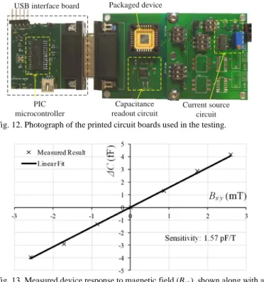
A photograph of the printed circuit boards used in the testing is shown in Fig. 12, illustrating the different functional sections. The measured magnetic field response of the device is presented in Fig. 13. The sensor exhibits a magnetic field sensitivity of 1.57 pF/T under static operation at a 10 mA current. The measured response shows a non-linearity of less than 6 % for the whole ±3 mT measurement range, where the non-linear error is calculated using
100 % . × − = fit linear fit linear result measured Errormeas . (16)
The measured non-linear error is a bit higher than the simulation results due to the non-linearity of the readout circuitry.
C. Acceleration Response
The inertial response of the fabricated devices is characterized by the same test circuitry used for magnetic field response, but with the current source circuit switched off. A picture of the test setup used is shown in Fig. 14. An Aerotech
Fig. 13. Measured device response to magnetic field (Bx/y), shown along with a
linear fit. Packaged device USB interface board
Capacitance readout circuit Current source circuit PIC microcontroller
Fig. 12. Photograph of the printed circuit boards used in the testing. 3.3 V Regulator Circuit VCS GND2 MAT14 SUB Rtune Rlimit ICS DUT VDD2 (3.3 V)
ARMS-200 rate table [16] is used for the test, where the packaged device is placed, along with the capacitive readout circuit, vertically using a right angle mount on the mounting arm at a distance r from the rate table center. The centrifugal acceleration generated by rate table rotation is utilized to measure the rate response of the device. The rate table angular speed, ω, is varied to generate the different acceleration steps for the test using (17) [17]. The centrifugal acceleration, Ac, is given by
2
c
A =mrω , (17)
where m is the proof mass. The digital capacitance data is then transmitted to the interface microcontroller circuit through the I2C interface via a 15 pin D-SUB cable and the rate table slip
rings, which maintain the electrical connectivity throughout rotation.
The measured acceleration response of the device is shown in Fig. 15. The sensor exhibits an acceleration sensitivity of 1.02 fF/g for static operation, with a non-linear error less than 10% in the range of ±2g.
The current test setup is limited to one axis being tested at a time. As such, different axis measurements can currently be achieved only by interfacing the test setup manually to the different pads of the device. The test setup could be augmented with an automated switching mechanism to allow for sequential testing of both axes without intervention.
VII. DISCUSSION
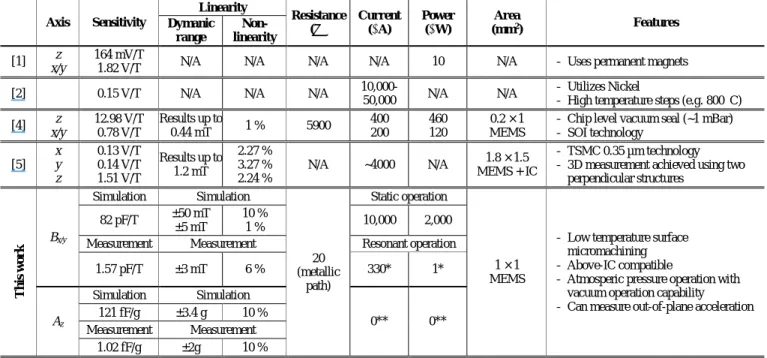
Table II compares the proposed device to state-of-the-art. The different units used to report the sensitivities are a result of the different readout schemes utilized. Piezoresistive readout is used in [1-2], while insufficient information is provided in [4-5] to extract the capacitance change.
Readout PCB with packaged device USB interface PCB ` Mounting arm Rate table r
Fig. 14. Picture of the test setup used for acceleration response characterization.
Fig. 15. Measured device response to out-of-plane acceleration (Az), shown
along with a linear fit.
TABLE II
COMPARISON BETWEEN THE COMBINED MAGNETOMETER/ ACCELEROMETER PROPOSED IN THIS WORK AND THE STATE-OF-THE-ART
Axis Sensitivity
Linearity
Resistance (Ω)
Current
(μA) Power (μW) (mmArea 2) Features Dymanic range Non-linearity [1] z x/y 164 mV/T
1.82 V/T N/A N/A N/A N/A 10 N/A – Uses permanent magnets
[2] 0.15 V/T N/A N/A N/A
10,000-50,000 N/A N/A
– Utilizes Nickel
– High temperature steps (e.g. 800 ◦C)
[4] z x/y 12.98 V/T 0.78 V/T Results up to 0.44 mT 1 % 5900 400 200 460 120 0.2 × 1 MEMS
– Chip level vacuum seal (~1 mBar) – SOI technology [5] x y z 0.13 V/T 0.14 V/T 1.51 V/T Results up to 1.2 mT 2.27 % 3.27 % 2.24 % N/A ~4000 N/A 1.8 × 1.5 MEMS + IC – TSMC 0.35 µm technology – 3D measurement achieved using two
perpendicular structures T h is wo rk Bx/y Simulation Simulation 20 (metallic path) Static operation 1 × 1 MEMS
– Low temperature surface micromachining – Above-IC compatible
– Atmosperic pressure operation with vacuum operation capability – Can measure out-of-plane acceleration 82 pF/T ±50 mT
±5 mT
10 %
1 % 10,000 2,000
Measurement Measurement Resonant operation
1.57 pF/T ±3 mT 6 % 330* 1* Az Simulation Simulation 0** 0** 121 fF/g ±3.4 g 10 % Measurement Measurement 1.02 fF/g ±2g 10 %
*Values estimated based on static operation measurements, while maintaining the same sensitivity.
In this work, the measurement results for sensitivity are lower than the simulated results mainly due to the bowing of the structure, as clear from the SEM micrograph in Fig. 1. This bowing causes an increase of the effective gap between the electrodes of the capacitor by a factor of ~10 and consequently reduces the capacitance variation and sensitivity by a factor of ~100. The bowing could be reduced by optimizing the device and suspension dimensions, and further tuning the stress profile of the material stack. Another cause for the sensitivity reduction lies in interconnect parasitics between the device and the readout circuitry, as discrete components were used for measurements. Fabricating the sensor directly above a full-fledged CMOS ASIC, as made possible by the fabrication process, is expected to allow for significant sensitivity improvements. Alternatively, wire bonding the device and the interface circuit within the same package could be used to reduce noise and parasitics (e.g., as demonstrated in [18] for a capacitive accelerometer). The metallic track below the structure leads to a low resistive path for the current (~20 Ω), which results in power dissipation and electrical noise reduction. Measurements were performed at a 10 mA current, which corresponds to 2 mW power dissipation. These values can be lowered, while maintaining good sensitivity, by reducing the bowing, and parasitics, as discussed earlier. They can also be significantly improved by using resonant operation. Based on the static operation measurements and a resonant mode with Q-factor of 30 (measured), the current required to keep the same sensitivity level will be reduced to ~330 μA, and the power consumption of the device is expected to be ~1 μW.
VIII. CONCLUSION
This work introduced a combined magnetometer / accelerometer design based on the Lorentz force, where an electrical current is switched between two orthogonal directions on the device structure to achieve a 2D in-plane magnetic field measurement. The device can concurrently serve as a 1D accelerometer for out-of-plane acceleration, when the current is switched off. The design is therefore capable of separating the magnetic and inertial force measurements, achieving higher accuracy with a single compact device. The proposed sensor supports static operation at atmospheric pressure, precluding the need for costly vacuum packaging. It can alternatively operate at resonance under vacuum for enhanced sensitivity. The device is fabricated using a low temperature SiC surface micromachining technology, which is fully adapted for above-IC integration on standard CMOS substrates. Measurement results from the fabricated device, using a discrete electronics interface, show a magnetic field sensitivity of 1.57 pF/T and an acceleration sensitivity of 1.02 fF/g for static operation.
The device could be further enhanced by adding lateral electrodes around the proof mass to allow for more axes of operation.
ACKNOWLEDGMENT
The authors would like to thank CMC Microsystems for providing the layout design tools and the testing equipment needed. The authors would also like to thank Mr. Don
Pavlasek from McGill’s mechanical workshop for his help on the mechanical test setup, and Mr. Karim Allidina for his support on the electrical test setup.
REFERENCES
[1] D. Ettelt et al., “A Novel Microfabricated High Precision Vector Magnetometer,” Proc. IEEE Conf. on Sensors, pp. 2010-2013, Oct. 2011. [2] M. El Ghorba, N. André, S. Sobieski, J. -P. Raskin, “CMOS Compatible
Out-of-Plane and In-Plane Magnetometers,” Proc. IEEE Conf. on
Solid-State Sensors, Actuators and Microsystems, pp. 2373-2376, June 2007.
[3] M. Thompson, M. Li, and D. Horsley, “Low Power 3-Axis Lorentz Force Navigation Magnetometer,” Proc. IEEE Conf. on MEMS, pp. 593-596, Jan. 2011.
[4] M. Li, V. Rouf, M. Thompson, and D. Horsley, “Three-Axis Lorentz Force Magnetic Sensor for Electronic Compass Applications,”
J. Microelectromech. Syst., vol. 21, no. 4, pp. 1002-1010, Aug. 2012.
[5] C. -I. Chang, M. -H. Tsai, Y. -C. Liu, C. -M. Sun, and W. Fang, “Development of Multi-Axis CMOS-MEMS Resonant Magnetic Sensor Using Lorentz and Electromagnetic Forces,” Proc. IEEE Conf. on MEMS, pp. 193-196, Jan. 2013.
[6] F. Nabki, T. Dusatko, S. Vengallatore, and M. El-Gamal, “Low-Temperature (<300oC) Low-Stress Silicon Carbide Surface
Micromachining Fabrication Technology,” Tech. Digest of the Hilton
Head Solid-State Sensors, Actuators and Microsystems Workshop, pp.
216 - 219, June 2008.
[7] F. Nabki, T. Dusatko, S. Vengallatore, and M. El-Gamal, “Low Stress CMOS-Compatible Silicon Carbide Surface-Micromachining Technology - Part I: Process Development and Characterization,”
J. Microelectromech. Syst., vol. 20, no. 3, pp. 720-729, June 2011.
[8] F. Nabki, P. Cicek, T. Dusatko, M. El-Gamal, “Low Stress CMOS-Compatible Silicon Carbide Surface-Micromachining Technology - Part II: Beam Resonators for MEMS above IC,” J. Microelectromech.
Syst., vol. 20, no. 3, pp. 730-744, June 2011.
[9] S. D. Senturia, Microsystem Design, Springer, 2001, pp. 136-217. [10] M. El-Gamal, P. -V. Cicek, F. Nabki, “Low temperature ceramic
microelectromechanical structures,” WO Patent 2010003228, 2010. [11] W.-H. Lin and Y.-P. Zhao, “Casimir Effect on the Pull-in Parameters of
Nanometer Switches,” Microsystem Technologies, vol. 11, no. 2-3, pp. 80-85, Feb. 2005.
[12]K. Ogata, “Transient and Steady-State Response Analysis,” in Modern
Control Engineering, 5th ed., Prentice Hall, 2010, pp. 172.
[13]ZSSC3123 cLiteTM Capacitive Sensor Signal Conditioner Datasheet, Rev. 1.61, Zentrum Mikroelektronik Dresden AG (ZMDI), Dresden, Germany, 2013.
[14]PIC18F2455/2550/4455/4550 Datasheet, Microchip Technology Inc., Chandler, AZ, 2009.
[15]MAT14 Matched Monolithic Quad Transistors Datasheet, Analog Devices Inc., Norwood, MA, 2010.
[16]ARMS Series Stage User Manual, Rev. 1.01.00, Aerotech Inc., Pittsburg, PA, 2011.
[17]J. R. Taylor, Classical Mechanics, University Science Books, 2005, pp. 344.
[18]A. Alfaifi, K. Allidina, F. Nabki, and M. El-Gamal, “A Low Cross-Sensitivity Dual-Axis Silicon-On-Insulator Accelerometer Integrated as a System In Package with Digital Output,” Analog Integrated Circuits and
Signal Processing, vol. 77, no. 3, pp. 345-354, 2013.
Mohannad Y. Elsayed (S’08) was born in Cairo, Egypt, in 1985. He received the B.Sc. degree with honors and M.Sc. degree in electronics and communications engineering from Cairo University, Giza, Egypt, in 2007 and 2010, respectively. He is currently working towards the Ph.D. degree at the Wireless Integrated Circuits and MEMS Laboratory, McGill University, Montreal, QC, Canada.
From 2007 to 2010, he was a Teaching Assistant with the Department of Electronics and Communications Engineering,
Cairo University, and a Research Assistant with the Yousef Jameel Science and Technology Research Center, The American University in Cairo, Cairo, Egypt. He has held internship positions with several institutions including Rice Automated Nanoscale Design Laboratory, Rice University, Houston, TX, and Thales, Canada. His research interests include MEMS devices and analog circuits, with special focus on MEMS sensors’ design, fabrication, the design of their interfacing electronics, and their monolithic integration with CMOS integrated circuits. He authored and coauthored nine journal and conference papers. He has filed three patents on novel circuit designs and MEMS devices.
Mr. Elsayed has held scholarships from McGill University and the Microsystems Strategic Alliance of Quebec (ReSMiQ).
Paul-Vahé Cicek (S’09) received the B.Eng. degree in electrical engineering (minor in arts) with distinction from McGill University, Montreal, QC, Canada, in 2006, where he is currently working toward the Ph.D. degree in electrical engineering.
He is currently a Researcher in the McGill Wireless Integrated Circuits and Microelectromechanical Systems (WICs & MEMS) Group, McGill University, where he interned in 2005 and 2006, developing a novel wafer-level packaging technology. His research interests include novelty MEMS design and fabrication, radio-frequency electronic design, advanced packaging and full monolithic integration of MEMS, and VLSI electronics.
Mr. Cicek was a recipient of scholarships from McGill University, the Quebec Fund for Research in Nature and Technology (FQRNT), the Microsystems Strategic Alliance of Quebec (ReSMiQ), and the Natural Sciences and Engineering Research Council of Canada (NSERC).
Frederic Nabki (S’99–M’10) received the B.Eng. degree in electrical engineering with honors and the Ph.D. degree in electrical engineering from McGill University, Montreal, QC, Canada, in 2003 and 2010, respectively.
In 2008, he joined the Université du Québec à Montréal (UQAM), Montreal, where he is currently an Associate Professor of microelectronics engineering. His research interests include microelectromechanical systems (MEMS) and RF/analog microelectronics, specifically focusing on the creation of next-generation MEMS processes using advanced materials, the integration of MEMS devices with CMOS systems, the modeling of MEMS devices, and the design of CMOS phase-locked loops, ultra-wideband transceivers, and MEMS interface circuits. He has published two book chapters and over 50 publications, and holds four issued patents and six pending patent applications related to MEMS and CMOS/MEMS monolithic integration.
Dr. Nabki is a member of the Quebec Order of Engineers. He was a recipient of the Governor General of Canada’s Academic Bronze Medal. He has held support from the Microsystems Strategic Alliance of Quebec (ReSMiQ), the Quebec Fund for Research in Nature and Technology (FRQ-NT), the Natural Sciences and Engineering Research Council of Canada (NSERC), and the Canada Foundation for Innovation (CFI).
Mourad N. El-Gamal (S’92–M’99) received the B.Sc. degree with honors in electrical engineering from Ain-Shams University, Cairo, Egypt, in 1987, the M.Sc. degree (minor in computer science) in electrical engineering from Vanderbilt University, Nashville, TN, in 1993, and the Ph.D. degree in electrical engineering from McGill University, Montreal, QC, Canada, in 1998.
He has held the William Dawson Scholar Chair in the Department of Electrical and Computer Engineering, McGill University, since 2004 and served as a member of the steering committee of the Nanofabrication facility of the Institute for Advanced Materials. He was an Associate Vice Principal- Research and International Relations (VP-RIR) of McGill University from March 2007 to July 2008. The office of the VP-RIR oversees all aspects of research activities at McGill, from science and engineering to biomedical and drug development. Among the main initiatives that he spearheaded was the development of a comprehensive university–industry partnership strategic plan, including all aspects of technology transfer and commercialization. In 2002, while on leave from McGill, he was the Director of Engineering and then the Vice President and General Manager of the Wireless Business Unit of MEMSCAP headquartered in France—a 165-employee publicly traded company specializing in microelectromechanical systems (MEMS). Earlier, he worked for IBM Research and for the French telecommunications company ALCATEL. He consults for companies and the Canadian Government on policies and strategies on regular basis. His research interests are in micro and nanoscale integrated electronics and mechanical systems, with a special interest in advanced materials. His research focus has been on the combination of these technologies to produce new knowledge and innovative solutions for a wide range of applications, including wireless communications systems, health care, and aerospace. He has published over 80 technical articles and three book chapters, and his team has received several research awards. He is the holder of one patent and currently has five patents filed on novel micro/nano processes and devices.
Dr. El-Gamal has been the recipient of numerous teaching awards. He was an Associate Editor of the IEEE TRANSACTIONS ON CIRCUITS AND SYSTEMS I from 2006 to 2008 and is currently the Chair of the Biomedical, Sensors, Displays, and MEMS subcommittee of the IEEE Custom Integrated Circuits Conference, formerly the Emerging Technologies subcommittee.