HAL Id: tel-02345743
https://tel.archives-ouvertes.fr/tel-02345743
Submitted on 4 Nov 2019HAL is a multi-disciplinary open access
archive for the deposit and dissemination of sci-entific research documents, whether they are pub-lished or not. The documents may come from teaching and research institutions in France or abroad, or from public or private research centers.
L’archive ouverte pluridisciplinaire HAL, est destinée au dépôt et à la diffusion de documents scientifiques de niveau recherche, publiés ou non, émanant des établissements d’enseignement et de recherche français ou étrangers, des laboratoires publics ou privés.
cryogenic temperatures and for a bio-medical application
Andrii Nagai
To cite this version:
Andrii Nagai. Investigation of SiPM physics parameters down to cryogenic temperatures and for a bio-medical application. Instrumentation and Detectors [physics.ins-det]. Université Paris Saclay (COmUE), 2016. English. �NNT : 2016SACLS552�. �tel-02345743�
Investigation of SiPM Physics
Parameters down to Cryogenic
Temperatures and for a Bio-medical
Application
Thèse de doctorat de l'Université Paris-Saclay préparée à l'Université Paris-Sud École doctorale n°576 Particules hadrons énergie et noyau :
instru-mentation, image, cosmos et simulation (PHENIICS) Spécialité de doctorat: imagerie médicale et radioactivité
Thèse présentée et soutenue à Orsay, le 22 septembre 2016, par
Andrii NAGAI
Composition du Jury: Achille Stocchi
Professor, Paris-Sud University, director of Linear accelerator laboratory Président
Gianmaria Collazuol
Assistant professor, University of Padova, Department of Physics and Astronomy Rapporteur
Christian Morel
Professor, Aix-Marseille University, Department of Physics Rapporteur
Adam Para
Dr., Fermi National Accelerator Laboratory, Semiconductor depatment Examinateur
Pascal Vincent
Dr., Sorbonne University, Pierre and Marie Curie Campus,
Laboratory of Nuclear Physics and High Energies Examinateur
Nicoleta Dinu-Jaeger
Abstract
Silicon PhotoMultiplier (SiPM) detector has become a suitable visible light/photon detector for many applications like high energy physics and neutrino experiments, fluorescence detection, bio-photonics and medical imaging. The main advantages are coming from its compactness (i.e. Si wafers ~300 µm thickness), easily adjustable size (i.e. from single to hundreds of readout channels), low operating voltage (i.e. Vbias < 80 V), high gain (i.e. G 105 ÷ 107), speed of response (i.e. tens of ps single photon timing resolution) and insensitivity to
magnetic fields (i.e. confirmed up to 7 T).
To achieve the best performance for a given application, two important points should be addressed: (1) device physics parameters like gain G, breakdown voltage VBD, signal shape, cell capacitance Cµcell, quenching resistance Rq, dark count rate DCR (i.e. thermal rate, afterpulses, cross-talk), photon detection efficiency PDE, and their temperature T variation should be known and their impact on the measurement quality must be understood, and (2) SiPM device with the best adapted technological and geometrical parameters should be selected.
During my thesis I have performed studies on various SiPM devices of the same cell size (50 × 50 m2) produced by two main manufacturers (i.e. Hamamatsu HPK and KETEK) and I
directed my analysis to improve our knowledge in the field of both previously mentioned points.
The first part of my thesis was oriented to the studies of SiPM physics parameters as a
function of temperature. Particularly, recent KETEK devices (year 2015) with different technological characteristics like p/n and n/p junctions, with and without trench technology, and different widths of epitaxial layer were studied in the temperature range from 308.15 K (+35 °C) down to 238.15 K (-35 °C). In addition, the Hamamatsu devices from 2011 production run as well as new devices from 2015 year, with improved technological characteristics inducing a reduced noise, were investigated in a wider temperature range from 318.15 K (+45 °C) down to 98.15 K (-175 °C).
For these purposes, I participated to the design, installation, commissioning and calibration of a cryogenic experimental setup dedicated to electrical, optical and temperature studies of SiPM devices. Also, I have developed an automatic analysis procedure able to handle in a short time an impressive quantity of experimental data (i.e. tens of Gb/device) and to give a precise and fast information on main SiPM parameters and their temperature dependence. In particular, a complete set of AC electrical parameters like gain G, breakdown voltage VBD, microcell capacitance Cµcell, pulse shape, quenching resistance Rq, dark count rate DCR and optical cross-talk were calculated. Detector properties like photon detection efficiency PDE and associated Geiger triggering probability PGeiger were also be evaluated.
I have also developed a physical model describing the DC I-V curves of SiPM detectors at different temperatures. The proposed model fits well the shape of IV curve in a very large currents range from 10-12 A up to 10-5 A over the full working range of various devices.
Consequently, the IV model can be used as a simple and fast method for determination of SiPM parameters like breakdown voltage VBD, the shape of Geiger triggering probability PGeiger as a function of Vbias as well as the Vbias working range. The comparison of these parameters with those calculated from AC measurements and analyzed by the automatic procedure showed a good agreement.
The second part of my thesis was oriented to the study of SiPM devices and their physical
parameters required to build a prototype of beta-sensitive intracerebral probe. Such probe is dedicated to measure the local concentration of radiolabeled molecules on awake and freely
moving animal and to study new animal models of human disorders (neurodegenerative diseases, tumor growth, and neuropsychiatric disorders). It is composed of small size, low-noise SiPM device coupled to a scintillating fiber and read-out by a dedicated miniaturized low-power consumption electronics. Three SiPM devices have been chosen as the most adapted for our application: two small KETEK devices of 0.5 × 0.5 mm2 size (with and without optical trenches,
specially developed by KETEK to fulfill our requirements) and a standard Hamamatsu device of 1.3 × 1.3 mm2 size, all devices having 50 × 50 μm2 μcell size. For each SiPM the gain G,
dark count rate DCR and beta sensitivity were measured as a function of Vbias and temperature. The obtained results showed that the small field of view and newly developed structure of the KETEK devices allow a large decrease of the dark count rate DCR. However, this small field of view also leads to a reduced light collection due to the thickness of the epoxy protection resin on top of the SiPM and the acceptance angle of the fiber. Since the beta sensitivity represents a tradeoff between photon detection efficiency PDE and dark count rate DCR, KETEK SiPMs exhibit similar performances in comparison with the Hamamatsu device. Preliminary results demonstrate that the beta sensitivity of KETEK devices can be significantly improved by using focusing lens between the scintillating fiber and the SiPM or by reducing the thickness of its epoxy protection resin.
Résumé
Les Photomultiplicateurs Silicium (SiPM) sont devenus aujourd’hui des détecteurs de lumière visible, applicables dans de nombreux domaines comme la Physique des Hautes Énergies, les expériences Neutrinos, la détection de fluorescence, pour des applications de bio-photonique ou d’imagerie médicale. Les principaux avantages de ces composants tiennent dans leur compacité (épaisseur des plaquettes de Si ~300μm), une surface de détection ajustable (de un à plusieurs centaines de canaux de lecture), un fonctionnement à faible tension de polarisation (i.e. Vbias < 80 V), un gain élevé (G 105 ÷ 107), une réponse rapide (quelques dizaines de picosecondes de résolution temporelle pour un photon), et une insensibilité aux champs magnétiques (jusqu’à 7 T).
Pour obtenir les meilleures performances pour une application donnée, il faut considérer deux points importants : (1) Les paramètres physiques comme le gain G, la tension de breakdown VBD, la forme du signal, la capacité de la μ-cellule Cμcell, la résistance de quenching Rq, le dark count rate DRC (i.e. : bruit thermique, afterpulses, diaphonie entre cellules) ainsi que leurs variations en fonction de la température doivent être connus, mais également leur impact sur la qualité de la mesure doit être comprise; (2) Le composant SiPM doit être sélectionné sur certains critères technologiques et sur l’adéquation de ses paramètres géométriques à l’application.
Durant ma Thèse, j’ai étudié plusieurs types de SiPM de même taille de μ-cellule (50 × 50 μm2) produits par deux sociétés (KETEK et HAMAMATSU), et j’ai concentré mes
analyses sur l’amélioration de nos connaissances concernant les paramètres mentionnés précédemment.
La première partie de ma Thèse concerne l’étude des divers paramètres physiques des
SiPM en fonction de température T. En particulier, des composants récents (2015) de KETEK ayant diverses caractéristiques technologiques comme des jonctions p/n ou n/p, avec ou sans trench entre cellules, différentes épaisseurs de couches épitaxiales, etc … ont été étudiés dans la gamme de T de 308.15 K (+35 °C) à 238.15 K (-35 °C). En plus, des composants Hamamatsu de production 2011, ainsi que de production 2015 avec des caractéristiques technologiques améliorées (faible bruit), ont été testés dans la gamme 318.15 K (+45 °C) à 98.15 K (-175 °C).
Pour ces études, j’ai participé à la conception, l’installation, la mise en service et la calibration d’un banc cryogénique destiné aux caractérisations électriques, optiques, et en température, des SiPM. J’ai développé une procédure d’analyse automatisée, capable de traiter en un temps très court une énorme quantité de données expérimentales (i.e. dizaines de Gb/détecteur), et de fournir une information rapide et précise sur les principaux paramètres et leur dépendance en T. En particulier, un set complet des paramètres électriques en AC, comme G, VBD, Cμcell, forme du signal, Rq et DCR furent calculés. Des paramètres comme la PDE et la probabilité de triggering PGeiger associée ont été également évalués.
J’ai développé un modèle physique décrivant les courbes IV en DC pour différentes T. Ce modèle proposé reproduit bien la forme de la courbe IV dans une large gamme de courants allant de 10-12 à 10-5 A sur toute la zone de fonctionnement des divers détecteurs. Ainsi, le
modèle IV peut être utilisé comme un outil simple et rapide pour déterminer les paramètres du SiPM comme le VBD, la forme de la courbe PGeiger en fonction de Vbias, ainsi que la plage des
tensions de fonctionnement. La comparaison de ces paramètres avec ceux obtenus en mesure AC, et analysés par la procédure automatisée, sont en bonne concordance.
La seconde partie de ma Thèse a porté sur l’étude de composants SiPM spécialement
adaptés à une application biomédicale. Il s’agit d’une sonde intracérébrale, sensible à l’émission β (Nβ) de molécules marquées par un traceur radioactif, injectées dans le cerveau d’un animal vivant. Le but étant de construire un nouveau modèle animal de maladies humaines telles que les maladies neuro-dégénératives ou neuropsychiatriques et la croissance de tumeurs. Cette sonde se compose d’un SiPM de très petite taille, bas bruit, couplé à une fibre scintillante, suivie d’une électronique de lecture spécifique, miniaturisée, à faible consommation. Ces SiPM ont été choisis comme les plus adaptés à notre application : deux SiPM de KETEK de 0.5 × 0.5 mm2
(spécialement développés par cette compagnie pour nos besoins), et un SiPM standard de 1.3 × 1.3 mm2 de Hamamatsu, tous ayant des μ-cellules de 50 × 50 m2. Pour chaque composant, les
paramètres G, DCR et la sensibilité β ont été mesurés en fonction de Vbias et T. Les résultats obtenus montrent que le faible champ de vue des nouvelles structures KETEK permet une bonne amélioration du DCR. Cependant ce faible champ de vue entraîne une perte de collection de lumière due à l’épaisseur de la couche de résine époxy de protection, et à l’angle d’acceptante de la fibre.
Comme la sensibilité β est un compromis entre le PDE et le DCR, les SiPM de KETEK montrent au final des performances voisines de celles de Hamamatsu. Les résultats préliminaires démontrent que la sensibilité β de KETEK peut être améliorée significativement en utilisant une lentille de focalisation entre la fibre scintillante et le SiPM, ou en diminuant l’épaisseur de la couche de résine époxy de protection.
Acknowledgements
First and foremost, I would like to express my sincere gratitude to my thesis advisor Nicoleta Dinu-Jaeger, You have been a tremendous mentor for me. It has been an honor and great opportunity to work with her. I appreciate all her contributions of time, ideas and funding to make my PhD experience productive. Without her guidance this dissertation would not have been possible. Nicoleta deserves very warm words for her patience in paying continuous attention to my scientific and nonscientific problems. I definitely can say that I caught a great opportunity to work with her as she is a good example of a successful physicist. Physicist who know how to manage the scientific work in all stages (e.g. planning and preparing the experiment, data taking, data analysis and presenting the results).
I would like to thank the reviewers Gianmaria Collazoul and Christian Morel who kindly agreed to spend part of their precious time and read this manuscript, their comments were very helpful and very much appreciated. Also, I would like to thank the rest of my thesis jury: Achille Stocchi, Adam Para and Pascal Vincent.
I would like to express my special appreciation and thanks to Adam Para. It is very hard to overestimate the importance of his advises and fruitful discussions during our meetings in Skype. His huge experience and knowledge in experimental physics and data analysis were extremely important and very much appreciated.
During my thesis I worked in collaboration with team from IMNC laboratory on a bio-medical application and therefore my sincere thanks also goes to IMNC laboratory: Laurent Menard, Laurent Pinot, Philippe Laniece, Marc-Antoine Verdier, Sara Spadola and many others.
Many thanks to LAL mechanical and infrastruction services for the precious help in designing and building the cryogenic set-up, as well as to SERDI/GRED group for providing lasers, measurement instruments and help in cabling. A special thanks is given to Hammoudi Nourredine from IPNO laboratory for his advises on calibration of the cryogenic set-up.
A lot of thanks to Jean-Jacques Jager for his patience, instruments and help with French language.
I would like to thank Sergey Barsuk for his useful advices and even more useful questions. Also, I would like to thank Elias Khan, Fabien Cavalier, Christiane Eder, Sylvie Prandt and all other people who helped me to resolve all administrative problems and as a result bring this thesis to the end.
I would like to thank all my friends with whom I had wonderful discussions with a cup of coffee every day at 16h00. In particular to: Leonid, Iryna, Viacheslav, Sviatoslav, Illya and Maksym.
Last but not the least, I would like to thank my family. To my parents and my brother who are always near and support me in all my pursuits and decisions. To my best grandfather in the world. Every hour which has been spent with you gave me a huge boost of energy for next months.
Table of contents :
Abstract ________________________________________________________________ - 1 - Résumé _________________________________________________________________ - 3 - 1. Introduction _________________________________________________________ - 9 - 2. SiPM - state of the art ________________________________________________ - 11 - 2.1. Precursors of SiPM – Photodiode, APD, GM-APD _____________________________ - 11 - 2.2. SiPM physics and technology _____________________________________________ - 19 - 2.2.1. Working principle ___________________________________________________________ - 19 - 2.2.2. Static characteristics _________________________________________________________ - 21 - 2.2.2.a. Forward IV characteristic ________________________________________________ - 21 - 2.2.2.b. Reverse IV characteristic _________________________________________________ - 22 - 2.2.3. Dynamic characteristics ______________________________________________________ - 25 - 2.2.3.a. Signal shape __________________________________________________________ - 25 - 2.2.3.b. Gain (G) ______________________________________________________________ - 27 - 2.2.3.c. Breakdown voltage (VBD) _________________________________________________ - 28 - 2.2.3.d. Dark count rate (DCR) ___________________________________________________ - 31 - 2.2.3.e. Optical cross-talk _______________________________________________________ - 34 - 2.2.3.f. Afterpulses ___________________________________________________________ - 37 - 2.2.4. Photon detection efficiency (PDE) ______________________________________________ - 39 - 2.2.4.a. Quantum efficiency (QE) _________________________________________________ - 39 - 2.2.4.b. Geometrical fill factor (ε) ________________________________________________ - 40 - 2.2.4.c. Triggering probability (PGeiger) _____________________________________________ - 40 - 2.2.4.d. Measurements of Photon Detection Efficiency (PDE) __________________________ - 42 - 2.2.5. Temperature dependence ____________________________________________________ - 44 - 2.2.5.a. Forward IV characteristic vs. T ____________________________________________ - 44 - 2.2.5.b. Reverse IV characteristic vs. T _____________________________________________ - 45 - 2.2.5.c. Signal shape vs. T ______________________________________________________ - 46 - 2.2.5.d. G vs. T _______________________________________________________________ - 47 - 2.2.5.e. VBD vs. T ______________________________________________________________ - 48 - 2.2.5.f. DCR vs. T _____________________________________________________________ - 50 - 2.2.5.g. Optical cross-talk vs. T __________________________________________________ - 52 - 2.2.5.h. Afterpulses vs. T _______________________________________________________ - 52 - 2.2.5.i. PDE vs. T _____________________________________________________________ - 53 - 3. Investigation of SiPM parameters down to cryogenic temperatures ___________ - 56 - 3.1. Experimental setup _____________________________________________________ - 56 - 3.1.1. Climatic chamber ___________________________________________________________ - 57 - 3.1.2. Electrical connections ________________________________________________________ - 57 - 3.1.3. Light injection ______________________________________________________________ - 58 - 3.1.4. Temperature Sensors (T sensors) _______________________________________________ - 58 - 3.1.5. Mechanical fixations _________________________________________________________ - 59 - 3.1.6. Temperature calibration ______________________________________________________ - 60 - 3.1.7. Read-out chain for DC / AC measurements _______________________________________ - 61 - 3.1.8. Remote operation: LabView automatic data acquisition program _____________________ - 62 - 3.2. Measured devices & measurements conditions ______________________________ - 64 - 3.3. Static characterizations _________________________________________________ - 66 -3.3.1. Forward IV characteristic vs. T _________________________________________________ - 66 - 3.3.2. Reverse IV characteristic vs. T _________________________________________________ - 68 - 3.4. Dynamic characterizations _______________________________________________ - 72 - 3.4.1. Automatic analysis procedure _________________________________________________ - 72 - 3.4.1.a. Waveform analysis _____________________________________________________ - 72 - 3.4.1.a.1. Waveform parameters _______________________________________________ - 72 - 3.4.1.a.2. Baseline restoration _________________________________________________ - 74 - 3.4.1.b. Pulse analysis _________________________________________________________ - 81 - 3.4.1.b.1. Pulse finding procedure ______________________________________________ - 81 - 3.4.1.b.2. Templates _________________________________________________________ - 82 - 3.4.1.b.3. Pulse characteristics _________________________________________________ - 83 - 3.4.1.b.4. Pulse identification __________________________________________________ - 85 - 3.4.1.b.5. Structure of a train of pulses and waveform simulation program ______________ - 86 - 3.4.1.b.6. Template subtraction procedure _______________________________________ - 87 - 3.4.1.c. Efficiency of automatic analysis procedure __________________________________ - 90 - 3.4.2. Properties of Poisson statistics for DCR & PGeiger calculation __________________________ - 91 -
3.4.3. Calculation of SiPM parameters ________________________________________________ - 93 -
3.4.3.a. G vs. Vbias vs. T _________________________________________________________ - 93 -
3.4.3.b. VBD vs. T ______________________________________________________________ - 95 -
3.4.3.c. G vs. ΔV vs. T __________________________________________________________ - 98 - 3.4.3.d. Cµcell vs. T _____________________________________________________________ - 99 -
3.4.3.e. Signal amplitude vs. Vbias vs. T ____________________________________________ - 103 -
3.4.3.f. DCR vs. DV vs. T ______________________________________________________ - 104 - 3.4.3.g. Optical cross-talk vs. DV vs. T ____________________________________________ - 108 - 3.4.3.h. PGeiger vs. DV vs. T ______________________________________________________ - 109 - 3.5. Physical model of the reverse IV characteristic _____________________________ - 112 - 3.5.1. Experimental data at room T fitted by the IV model _______________________________ - 114 - 3.5.1.a. Dark conditions _______________________________________________________ - 114 - 3.5.1.b. Light conditions _______________________________________________________ - 117 - 3.5.2. Experimental data at various T fitted by IV model _________________________________ - 119 - 3.5.2.a. Dark conditions _______________________________________________________ - 119 - 3.5.2.a.1. VBD vs. T __________________________________________________________ - 121 - 3.5.2.a.2. Working range vs. T _________________________________________________ - 122 - 3.5.2.a.3. PGeiger-DC vs. T ______________________________________________________ - 123 - 3.5.2.b. Light conditions _______________________________________________________ - 125 - 3.5.2.b.1. VBD vs. T __________________________________________________________ - 126 - 3.5.2.b.2. Working range vs. T _________________________________________________ - 127 - 3.5.2.b.3. PGeiger vs. T ________________________________________________________ - 128 - 4. Investigation of SiPM parameters in a bio-medical context _________________ - 131 - 4.1. Introduction _________________________________________________________ - 131 - 4.1.1. Principle of beta-sensitive intracerebral probes __________________________________ - 131 - 4.1.2. “Sonde IntraCerebrale” SIC __________________________________________________ - 132 - 4.1.3. Pixelated intracerebral probe PIXSIC ___________________________________________ - 133 - 4.2. New miniaturized probe for charged particles detection in molecular imaging based on SiPM (SONIM) ______________________________________________________________ - 135 - 4.2.1. SiPM devices for SONIM project ______________________________________________ - 136 - 4.2.2. Experimental setup _________________________________________________________ - 137 - Miniaturized electronics __________________________________________________________ - 138 - 4.2.3. Test procedure ____________________________________________________________ - 140 - SiPM characterization using LAL cryogenic setup ______________________________________ - 141 -
Calibration of DCR measured using the LAL and IMNC setups ____________________________ - 143 - Determination of SiPM position for light collection optimization __________________________ - 145 - 4.2.4. Experimental results ________________________________________________________ - 147 - 5. Summary of SiPM parameters investigations and perspectives ______________ - 151 - 5.1. Summary ____________________________________________________________ - 151 - 5.2. Perspectives _________________________________________________________ - 153 - A. Resume __________________________________________________________ - 155 - Annex 1 – Static measurements ___________________________________________ - 163 - Forward measurements __________________________________________________________ - 163 - Reverse measurements __________________________________________________________ - 164 -
Annex 2 - PGeiger measurements ____________________________________________ - 169 -
Annex 3 – Numerical TCAD C-V simulation ___________________________________ - 173 -
Annex 4 - PGeiger parameterization __________________________________________ - 175 -
Thesis results __________________________________________________________ - 179 -
List of the papers published on the thesis results __________________________________ - 179 -
List of the conferences attended presenting the results of the thesis __________________ - 179 -
1. Introduction
Silicon PhotoMultiplier (SiPM) detector has become a suitable photon detector for many applications that would employ typically PMTs or MA-PMT. Thanks to its important advantages such as compactness (i.e. Si chips ~300 µm thickness), easily adjustable size (i.e. from single to hundreds of readout channels), low operating voltage (i.e. < 80 V), high gain (i.e. 105 – 107), speed of response (i.e. tens of ps single photon timing resolution) and insensitivity
to magnetic field (i.e. confirmed up to 7 T), the SiPM is used today in many applications like high energy physics [1] and neutrino experiments [2], fluorescence detection [3], and biophotonics [4] and medical applications [5] [6].
To achieve the best performances for a given application, two important points should be addressed:
SiPM physics parameters like gain, breakdown voltage, signal shape, dark count rate (i.e. thermal rate, afterpulses, cross-talk), photon detection efficiency, and their temperature variation should be known, and their impact on the measurement quality should be understood;
a SiPM device with the best adapted technological and geometrical parameters should be selected.
During my thesis I directed my work to improve our knowledge in the field of both previously mentioned points. More precisely, I performed studies on various SiPM devices of the same cell size (50 × 50 m2), with different technological characteristics, produced by two
main manufacturers (i.e. Hamamatsu HPK and KETEK) and I analyzed their parameters in a context of temperature and bias voltage variation and for a biomedical application.
An overview of SiPM physics and technology, as well as the present state of the art of its various physics parameters is given in the Chapter 2 “SiPM - state of the art”. In particular, static characteristics as forward and reverse current-voltage IV curves, dynamic characteristics as signal shape, gain, breakdown voltage, dark count rate, cross-talk and afterpulsing, and optical parameter as photon detection efficiency including quantum efficiency, geometrical fill factor and triggering probability are described in detail. Moreover, the present knowledge on their temperature dependence is also presented.
The main part of my thesis was oriented to the study of the physics parameters of various SiPM devices as a function of temperature and bias voltage, in dark and light conditions, and it is included in the Chapter 3 “Investigation of SiPM parameters down to cryogenic temperatures”. Particularly, I studied SiPM’s from 2015 production year runs with:
different technological characteristics like p/n and n/p junctions, with and without trench technology, and different widths of epitaxial layer produced by KETEK company; these devices were tested in a temperature range from 308.15 K (+35 °C) down to 238.15 K (-35 °C).
improved technological characteristics inducing a reduced noise produced by Hamamatsu company; these devices were tested in a wider temperature range from 318.15 K (+45 °C) down to 98.15 K (-175 °C); for calibration and comparison purposes, an old Hamamatsu device from 2011 production run was also tested in the same conditions.
In this context, the cryogenic setup developed at the Laboratory of Linear Accelerator (LAL) as well as various elements of particular relevance for our measurement like climatic chamber, electrical connections, light injection, temperature sensors, mechanical fixations, temperature
calibration etc… are described in detail in the Section 3.1 “Experimental setup” and Section 3.2 “Measured devices & measurements conditions”.
The main physics results of the thesis are presented in the Sections 3.3 “Static characterizations” and 3.4 “Dynamic characterizations”. In particular, the temperature dependence of forward and reverse IV characteristics allowing to calculate the quenching resistance and respectively the breakdown voltage are given in the Sections 3.3.1 and respectively 3.3.2. Moreover, the temperature and bias voltage dependence of various AC electrical parameters as gain, breakdown voltage, capacitance, signal amplitude, dark count rate, optical cross-talk and Geiger triggering probability are given in the Section 3.4.3.
Since the analysis of SiPM AC parameters in various temperature and bias voltage experimental conditions involved a huge amount of experimental data (tens of Gb/device), an automatic procedure able to handle these data in a very short time and to extract the parameters of interest was developed on ROOT data Analysis Framework and it is described in detail in the Section 3.4.1 “Automatic analysis procedure”. In particular, the general waveform parameters and the procedure for baseline restoration are given in the Sections 3.4.1.a.1 “Waveform parameters” and respectively 3.4.1.a.2 “Baseline restoration”. Various steps involved in the analysis of SiPM pulse analysis like pulse finding procedure, pulse template, pulses characteristics and identification, trains of pulses and template subtraction procedure are described in the Section 3.4.1.b, while the efficiency of the analysis procedure is related in the Section 3.4.1.c.
A fully new physical model describing the shape of reverse IV characteristics was developed and it is presented in the Section 3.5. This model allows fast calculation of three important SiPM parameters like breakdown voltage, working range and the shape of Geiger triggering probability. The results of these parameters extracted from experimental IV curves fitted by our model are presented in the Sections 3.5.1 (room temperature) and 3.5.2 (various temperatures). The second and quite modest part of my thesis was oriented to the study of SiPM devices dedicated to a beta sensitive intra-cerebral probe and it is presented in the Chapter 4, “Investigation of SiPM parameters in a bio-medical context”. A short introduction describing the detection principle and the limitations of previously developed beta probes is given in the Section 4.1 “Introduction”. Details on the new miniaturized probe based on SiPM and its principle are presented in the Section 4.2. The selected SiPM devices selected (two small devices of 0.5 × 0.5 mm2 specially developed by KETEK company at our request, and a
standard Hamamatsu device of 1.3 × 1.3 mm2) are presented in the Section 4.2.1 “SiPM devices
for SONIM project”. The experimental setup developed in collaboration with our colleagues from the laboratory of “Imagerie et Modelisation en Neurobiologie et Cancerologie” and dedicated to characterize the SiPM physics parameters of interest for this application (dark count rate, beta sensitivity) as well as the miniaturized dedicated read-out electronics developed at LAL are described in the Section 4.2.2 “Experimental setup”. The test procedure and the obtained experimental results are given in the Section 4.2.3 “Test procedure” and 4.2.4 “Experimental results”.
The manuscript of the thesis is finishing with the Section 5, “Summary of SiPM parameters investigations and perspectives” including the main results of the thesis and future perspectives.
2. SiPM - state of the art
In this Section, a review of various silicon devices developed up today and dedicated to visible light detection will be given. Primary, the technological structures and the light detection principle of the well-known Photodiode (PN or PIN), Avalanche Photodiode (APD) and Geiger-Mode Avalanche Photodiode (GM-APD) will be related. Then, the attention will be focused on the most recent silicon photon detector, the so-called Silicon PhotoMultiplier (SiPM), device to which my thesis studies were particularly dedicated. The SiPM technological structures, its static (e.g. forward and reverse current-voltage IV curves) and dynamic characteristics (e.g. signal shape, gain, breakdown voltage, dark count rate, cross-talk and afterpulsing) and photo-detection efficiency will be described in details. Since the temperature variation of many SiPM parameters is important for many applications, a particular attention to the temperature dependence of the SiPM parameters will be given. This overview is based on some reference publications, with the aim to learn what has been already known in the field before starting my PhD thesis and to motivate the choice of the work and futures studies I have performed during my thesis.
2.1. Precursors of SiPM – Photodiode, APD, GM-APD
For a better understanding of the main reasons for which the SiPM was developed as photon detector as well as for an easier transition to the physical phenomena’s involved in the SiPM, a short review of its ancestors will be given below.
Photodiode
A photodiode device is using the functionality of reversed biased p-n junction to detect light. The cross section of a generic Si photodiode is presented in Figure 2.1 [7]. The p-type impurity is shallow diffused at the active surface of n-type Si substrate to form the p-n junction (typical thickness of the p-type layer is 1 µm or less). The contact pads are deposited, the positive electrode (anode) on the front of active area and the negative electrode (cathode) on the back side. To reduce the light loos due to light reflection the active area is passivated with an antireflection coating.
When the photons with an energy greater than bandgap energy Eg (EgSi = 1.12 eV which corresponds to a wavelength of 1100 nm) strike a device, the valence band electrons are excited to the conduction band, leaving holes in their place in the valence band. Because of presence of internal electric field inside the junction, the electrons and holes drift in opposite directions to device electrodes. The number of collected charges is proportional to the intensity of the incident light, and therefore a photodiode is a device with an internal gain of 1.
Because of their simplicity, the photodiodes are used today in many applications, particularly where photomultipliers tubes are too bulky and delicate, or where high voltage is not possible to be applied or where insensitivity to magnetic fields is required. However, because of their lack of internal gain, the smallest detectable light flux should be at least 108 ÷ 109 photons/s.
In a first approximation, the photodiode current can be described by the Shockley ideal diode law:
1 exp T j s V V I I 2.1
where Is – is the reverse biased saturation current, Vj – is the voltage across the junction, VT – is the thermal voltage (VT = kT/q, where k – is the Boltzmann constant, T – is the temperature and q – is the elementary charge), η – is the ideality factor (has a value of 1 for the diffusion current and is approximately 2 for the recombination current).
The dark IV characteristic is presented by the curve (1) in Figure 2.2 [7]. However, when the light illuminates the photodiode, the curve (1) shifts by the amount of photocurrent Iph which is proportional to the photon flux (curves (2) or (3)). Thus:
ph T j s I V V I I exp 1 2.2
Figure 2.1 The cross section of generic Si photodiode [7] Figure 2.2 Current-voltage characteristic for a photodiode in dark (1) and light conditions (2) and (3) [7]
A photodiode can be operated either in photovoltaic mode (unbiased) or in photoconductive mode (few volts reverse biased voltage).
The photodiode optical performance is characterized by the responsivity Rλ and quantum efficiency QE. Rλ is the effectiveness of the conversion of the light power Popt into electrical photodiode current Iph: opt ph P I R 2.3
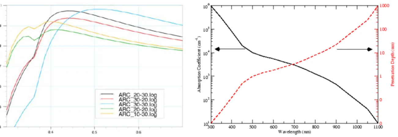
The Rλ varies with the incident light wavelength λ, applied bias voltage and temperature T. The Rλ as a function of λ for various photodiodes produced by Hamamatsu is presented in Figure 2.3 [7]. The photodiode QE is defined as the ratio between the incident photons to photons that contribute to photocurrent. It is connected to Rλ as:
R e c h R QE 1240 2.4
where h – is the Plank constant, c – is the light speed in the vacuum, e- – is the electron charge, Rλ – is the responsivity in A/W and λ – is the wavelength in nm. As can be observed in Figure 2.3 the QE has maximum of 65 ÷ 90% for an 800 ÷ 900nm wavelength range.
Figure 2.3 Rλ as a function of λ for various
photodiodes produced by Hamamatsu [7]
The photodiode is considered linear if the Iph increases linearly with the Popt. The lower limit of linearity is limited by the noise dark current Itn. The Itn is the sum of the thermal noise (or Johnson noise) IJn and the shot noise Isn:
2 2 sn Jn tn I I I 2.5
The upper limit of photodiode linearity is limited by the diode series resistance and the load resistance.
The photodiode characteristics are affected by change in temperature. The most affected ones are: dark current, shunt resistance, and responsivity. The dark current is approximately double for every 8 ÷ 10 0C increases in temperature. The shunt resistance may double for every
6 0C decreases in temperature. The variation of responsivity is related to absorption coefficient
which changes with temperature.
Avalanche Photodiode (APD)
An APD is also using the functionality of silicon p-n junction to detect light. The mechanism by which carriers are generated inside an APD is the same as in a photodiode, but the APD is different from a photodiode in that it has a functionality to multiply the generated internal current.
An APD is designed to work at higher reverse bias voltage (e.g. tens to hundreds of volts), which leads to an electrical field inside the p-n junction one order of magnitude higher than the photodiode (See Figure 2.4) and riches up to 105 V/cm. Therefore, if the electrical field is high
enough, the primary generated carriers accelerate and gain enough energy to ionize the crystals lattice with the subsequent production of the secondary electron-hole pairs, phenomena called impact ionization. The secondary pairs will be accelerated and can multiply too. This
phenomena is called “avalanche multiplication” and it is used by APD if it is reverse biased at enough high voltage, approaching the breakdown voltage. The multiplication rate (number of generated charges) due to impact ionization is given by the equation:
p p n
n J J
M 2.6
where αp, αn – are the holes and electrons ionization rates respectively, Jp, Jn – are the hole and electron current densities.
The APD gain or multiplication rate M increases the internal photo-electric signal. Therefore, the output current is expressed as:
opt
APD M R P
I 0 2.7
where R0(λ) – is the intrinsic responsivity of the APD at a gain M = 1, λ – is the wavelength, M – is the gain of the APD and Popt – is the incident optical power. The gain of APD varies with applied reverse voltage Vbias. The gain-voltage curve of APD produced by Hamamatsu (S12023-05) is presented in Figure 2.5. The optimal gain depends in part on the excess noise factor F: 2 2 2 M M F M 2.8
where σM – is the gain variation. We can observe that APD’s can reach gains of the order of 500 ÷ 1000, and therefore, with special designs, APD’s may improve the signal-to-noise ratio with respect to Photodiode and increase the sensitivity by at least two orders of magnitude (e.g. photon flux of tens to hundreds of photons can be detected).
Figure 2.4 Schematic representation of an APD and internal electrical field [7]
Figure 2.5 An APD (Hamamatsu S12023-05 device) gain as a function of reverse voltage [7]
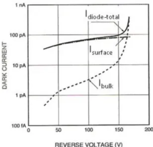
The dark current for an APD can be described in a first approximation by the Shockley ideal diode law given by Eq. 2.1. But it gives only a qualitative agreement with reverse current-voltage IV characteristics of real device. The real APD device`s dark current Idiode-total consists of the sum of surface leakage current Isurface flowing through the interface between the p-n junction and Si oxide layer existing on the diode surface and the internal current Ibulk generated inside of the Si substrate multiplied by the multiplication factor M:
bulk surface
total
diode I M I
I 2.9
The Ibulk flows in the avalanche region so it is multiplied by the APD gain M, whereas Isurface doesn`t flow in the avalanche region and therefore is not multiplied. The contributions of Isurface and Ibulk to the total Idiode-total as a function of Vbias for a classical APD is presented in Figure 2.6 [7]. We can observe that the Ibulk increases much faster with respect to Isurface with increasing Vbias due to increases of M, as was expected from Eq. 2.9.
Figure 2.6 Dark current vs. reverse voltage for a classical APD device; the contributions of surface leakage current Isurface
and the bulk generated leakage current Ibulk are showed [7]
The APD characteristics, similar to photodiode`s, are affected by temperature changes. In particular, the APD gain variates with temperature with a temperature coefficient of:
C dT dM M 0 %/ 2 . 2 1 2.10
Geiger Mode Avalanche Photodiode (GM-APD)
As we will see in the Section 2.2, the GM-APD represents the elementary cell of SiPM, therefore its structure and physical properties will be described in details in the following.
As its predecessors, the GM-APD structure is also based on a p-n junction, but it is designed in such a way that it works at reverse bias voltage exceeding the breakdown voltage and consequently, the electrical field inside the junction reaches high values of the orders of 3÷9×10⁵V/cm. That means that each single carrier created by an incident photon gain enough
energy to trigger an avalanche with a multiplication factor close to infinity (M = ). Such condition is called Geiger mode. Historically, the first GM-APD devices have been proposed by Haitz (Haitz, 1964, 1965) and McIntire (R. McIntyre, 1961, 1966) in their studies of micro-plasma instabilities. The proposed structures are quite different and they are presented in Figure 2.7.
Figure 2.7 GM-APD devices proposed by Haitz, 1965 a) and McIntyre, 1966 b)
The first one shown in Figure 2.7 a) represents a so-called thin-junction GM-APD structure with an optical window on top side and an avalanche region (high electrical field) formed by the n+ layer with the p-type substrate. An n- guard ring is used to isolate and create a small, well
defined avalanche region. Such kind of device has two main features: low breakdown voltage of 20 ÷ 50 V and small active area of 20 ÷ 100 µm in diameter.
The second one shown in Figure 2.7 b) represents a so-called thick-junction GM-APD structure with an optical absorption window on the bottom and the avalanche region formed by the n+p+ layer on the top. Typically, the avalanche region thickness extends more than 10 µm.
Such kind of devices has three main features: breakdown voltage of 200 ÷ 500 V, wide active area of 100 ÷ 500 µm in diameter and high avalanche current of few tens of mA. These devices are delicate and costly, therefore not widely presented. The actual GM-APD devices are mainly based on the structure initially developed by Haitz.
Following the McIntyre (R. McIntyre, 1961) the operation of GM-APD can be qualitatively described as in Figure 2.8. In this representation the GM-APD is biased to Vbias above the breakdown voltage VBD. It will stay in an OFF state (no current is flowing) until a carrier will trigger an avalanche what will bring the device into its ON state (current increases). Not every carrier in the depletion region will initiate an avalanche, therefore the probability to trigger an avalanche is characterized by the triggering probability PGeiger (more details in chapter 2.2.4). To be able to detect next photon, the avalanche current must be turned off by using proper quenching mechanism, able to reduce the bias voltage to VBD or below, and finally recharge it to initial Vbias.
Figure 2.8 Qualitative description of the operating mechanism of GM-APD
Few different mechanisms can be used to quench the avalanche. The simplest one, the so-called passive quenching, is by using a high ohmic resistor (hundreds of kΩ) in series with the GM-APD [8] (See Figure 2.9 a)). Also, an active quenching mechanism presented in Figure 2.9 b), and composed by an active resistor made on MOS transistor controlled by fast trigger electronics [8] can be used.
Figure 2.9 Schematic representation of GM-APD connected to passive a) and active b) quenching mechanism [8]
Since the quenching mechanism involved in SiPM µcells is the passive one, I will describe in more details the dynamic behavior of a GM-APD quenched by a quenching resistance. Starting from the electrical model developed by Haitz [9] and presented in Figure 2.10, the GM-APD can be presented as a diode resistance RD and a capacitance CD, connected in series to a quenching resistance RQ (passive quenching mechanism). The switch S represents the GM-APD into its OFF state (before avalanche multiplication) and into its ON state (carrier triggers an avalanche). The time evolution of current ID and voltage VD across the GM-APD during the avalanche evolution are presented in Figure 2.11.
During the pre-avalanche state (t < t0) the CD is charged at VD = Vbias > VBD and no current is flowing through the circuit. When a carrier triggers an avalanche (t = t0), the new state of the GM-APD can be modeled by turning ON the switch S (the VBD and RD added to the circuit). Following Haitz [9] and Senitzky [10], at t = t0 a very short current spike of ~10-11 s occurs through the diode, with a maximum current of (Vbias - VBD)/RD. In the same time, the CD discharges exponentially from VD = Vbias - VBD to VBD through RD with a time constant
τdischarge = RD × CD. At t = t1 when the CD is discharged and VD is reached to VBD, the current flows to an asymptotic value of (Vbias - VBD)/(RD + RQ). If the value of RQ is big enough, it will let the ID decreases to a level smaller than a critical value called Ilatch and the avalanche will be quenched. The Ilatch represents the current below which the population of the carriers is enough small that they will transit out of the high-field region without ionizing. The probability that the current is so low that statistical fluctuation brings the instantaneous number of carriers flowing through the high-field region to zero and consequently quenches the avalanche is called turn-off probability Pturn-off.
Figure 2.10 Equivalent circuit of a GM-APD [9] Figure 2.11 Time evolution of the avalanche current signal and the voltage across the GM-APD [9]
As the avalanche multiplication is quenched, the switch S is again in OFF position (t > t1). The CD which was discharged at VBD (during the avalanche multiplication) starts the recharging to its normal state of Vbias through RQ with a time constant τrecharge = CD × RQ. The total recharge time, defined as the time needed to recharge the diode from 0 to 99% of the bias voltage is given as: 5 × τrecharge = 5 × CD × RQ. Since the RQ >> RD the recharge time is much longer than the discharge: τrecharge >> τdischarge. During the time interval from t1 to t2 the device can work and detect a new photon, but since the CD is not fully recharged the GM-APD gain will be limited by: e rech normal t G t G arg exp 1 ) ( 2.11
where G(t) – is the GM-APD gain in t1 < t < t2, Gnormal – normal device gain when the CD is charged to Vbias. The G increases with increasing Vbias and can reach a typical gain of PMT`s ~106. The GM-APD will be operable with a normal gain only at t > t
2 therefore the device dead time tdead is defined as:
Q D e rech dead t t C R t 2 0 5 arg 5 2.12
A typical tdead of a GM-APD is in a range from few tens up to few hundreds of ns as a function of device RQ and CD.
As shown in this section, employing the avalanche breakdown mechanism the GM-APD becomes the first detector in silicon technology which provides high gain, comparable with that of the photomultiplier tubes. Thanks to this property, the GM-APD allows the detection of single photon, reason for which it is also called single-photon avalanche photodiode (SPAD) [11]. However, the tdead limits the GM-APD dynamic range and it cannot provide proportional
information regarding the magnitude of an incoming photon flux. Therefore, to overcome this limitation, new devices called the SiPM`s were invented by Golovin and Sadygov [12] [13] and they will be presented in details in the following section.
2.2. SiPM physics and technology
2.2.1. Working principle
The SiPM structure is composed by a parallel array of µcells on a common silicon substrate, where each µcell is a GM-APD connected in series with a Rq. A top view to a commercial device of 1 × 1mm2 total area with 400 µcells of 50 × 50 µm2 size is presented in Figure 2.12.
Two electrodes are shown on the top of the device, one is connected through a metallic grid to µcells and another one to the common substrate. A detailed cross-section of a typical device is presented in Figure 2.13. The µcells are shown, each of them being represented by a p-n junction built on a thin (1 ÷ 4 µm) epitaxial layer grown on a Si substrate. Individual Rq is connecting each µcell with the metal grid. The active area is covered by an antireflection coating to optimize the detection of light with a given wavelength.
To use the SiPM as a low light level detector an external amplifier should be connected to the device. An example of connection of the SiPM to an amplifier is presented in Figure 2.14 [7]. The 1 kΩ resistance and 0.1 µF capacitance serve as a low-pass filter that eliminates high frequency noise of the power supply. An oscilloscope connected to the amplifier`s output is the easiest way to observe the signals from the SiPM. An example of typical output SiPM signals coming from different µcells is presented in Figure 2.15. The situations where one, two and three fired µcells are shown. Each µcell works as a digital device, and gives a standard output signal independent of the number of photons which fired the device (no information on light intensity). However, all µcells are connected together in parallel on a common load, producing an output signal which is the sum of signals from all fired µcells (the SiPM works as an analog device; it can measure the light intensity).
Figure 2.13 Schematic drawing of a typical SiPM device
1m
mm
1m
m
Figure 2.12 Picture of SiPM detector produced by Hamamatsu HPK, with a total area of 1x1 mm2 and µcell
of 50 × 50 µm2; a metallic grid is connecting the µcells in
Figure 2.14 Example of connection of the SiPM to an
amplifier [7] Figure 2.15 Typical output signals, We can distinguish a signal from single µcell, two, three and four fired µcell in the same time
The SiPM’s presented today on the market can be classified in two main technological categories: (1) devices with n+/p µcells build on p-type substrate, produced by FBK (e.g. RGB
SiPMs) and SensL (e.g. M-series) and (2) devices with p+/n µcells build on n-type substrate,
produced by FBK (e.g. NUV SiPMs), Hamamatsu, KETEK, and SensL (e.g. B-series). The main difference of these two categories is that the first one is more sensitive to green light, whereas the second one is more sensitive to blue light (more details will be given in the Section 2.2.4 “Photon detection efficiency (PDE)” the two types of structures are schematically represented in Figure 2.16 a) and b) [14]. For both structures, device sizes of 1 × 1 mm2,
2 × 2 mm2, 3 × 3 mm2 and 6 × 6 mm2 with different µcell size from 10 µm to 100 µm are
available. Small µcell size leads to a higher dynamic range at the expense of geometrical fill factor which leads to a decrease of photon detection efficiency (see Section 2.2.4 “Photon detection efficiency (PDE)”).
Figure 2.16 Schematic representation of two categories of SiPM µcells and the corresponding electrical field shape: a) FBK (RGB SiPMs) and SensL (M-series) devices (µcells of n+/p/p-epi/p substrate); b) Hamamatsu devices (µcells of p+/n/n-epi/n
substrate) [14]
Besides the main difference in between these two categories mentioned previously, inside of a given category the SiPM parameters vary from one producer to another as well as from one device to another. Therefore, for a good selection of the most adapted device as well as for achieving the best performance to a given application, the most important SiPM parameters like gain, breakdown voltage, signal shape, dark count rate, and photon detection efficiency should be known. Majority of these parameters can be determined from dynamic measurements (the so-called AC tests), with an expenses of a quite complicate experimental setup (it requires an amplifier and a data acquisition system). However, a much faster and simpler static current-voltage measurements (so-called DC tests), requiring just a connection of the device to a
source-meter, can be used to easily measure parameters like breakdown voltage, device working range and quenching resistor Rq. Moreover, the reverse IV characteristic can be also used to determine
the shape of the Geiger probability, one of the SiPM parameter which is not yet fully understood in our days.
I should mention here that the number of scientific publications reporting on the characterization of SiPM devices and on the analysis of their parameters increased exponentially since last 10 years and a detailed overview is almost impossible to be given in this short chapter of my thesis. However, a modest summary of SiPM parameters extracted from some reference publications will be given, showing that many physical phenomena related to this device are already known today, but still more work is required for a full understanding of some of them.
2.2.2. Static characteristics
2.2.2.a. Forward IV characteristic
The forward IV characteristics of various SiPM`s produced by Hamamatsu HPK, SensL, FBK and KETEK are presented in Figure 2.17[15] and Figure 2.18 (A. Nagai, not published). Independent of device, we can observe that IV curve is characterized by a very small increase of the forward current with the Vbias up to a given Vcr (e.g. 0.6 V for Hamamatsu, KETEK and FBK devices; 6 V for SensL devices) and a much faster and linear increase of the current for Vbias exceeding Vcr.
Figure 2.17 Forward static characteristics of the different SiPM`s produced by Hamamatsu HPK, SensL and FBK [15]
Figure 2.18 Forward static characteristics of the different SiPM`s produced by KETEK (A. Nagai, not published)
For a physical interpretation of these results, we can start from the ideal Shockley low and express the forward current flowing through a p-n diode as following by Eq. 2.1. From this equation the Vj can be expressed as:
1 ln s T j I I V V 2.13
The voltage Vj is the difference between the applied voltage Vbias and the voltage drop across the neutral region and the ohmic contacts on the two sides of the junction IRs:
Vj = Vbias - IRs 2.14 Replacing Vj by Vbias in the Eq. 2.13, we obtain:
s s T Bias IR I I V V ln 1 2.15
Since the SiPM is composed by a given number of µcell`s Nµcell, where each of µcell is presented as a diode (GM-APD) connected in series with a quenching resistor Rq, the Eq. 2.15 can be implemented for a single SiPM µcell by adding an additional voltage drop on quenching resistance Rq: q s s T Bias IR IR I I V V ln 1 2.16
or for full SiPM device with Nµcell, where each µcell is connected in parallel:
cell q cell s s T Bias N R I N R I I I V V ln 1 2.17 The 𝐼 𝑅𝑠 𝑁𝜇𝑐𝑒𝑙𝑙+ 𝐼 𝑅𝑞
𝑁𝜇𝑐𝑒𝑙𝑙 term remains negligible when I is small, however it dominates at high
currents (I > 10 mA). As the result the Rs + Rq of a SiPM can be calculated from linear fit (I = a + b × Vbias, where a and b – are the fit free parameters) of the forward IV plots presented in Figures 2.18 and 2.19: b N R R R R Rq q s q s cell 2.18
where Nµcell – is the number of the SiPM µcells. Consequently, Rq ranging from 70 kΩ for Hamamatsu HPK up to 770 kΩ for KETEK devices have be found.
2.2.2.b. Reverse IV characteristic
The reverse IV characteristics of different SiPM`s produced by Hamamatsu HPK, SensL, FBK and KETEK are presented in Figure 2.19 [15] and Figure 2.20 [16]. We can recognize the value of VBD ~22.5 V for KETEK devices, the VBD 28 ÷ 32 V for SensL and FBK devices and the VBD ~69 V for the Hamamatsu devices. Independent of the device and producer, the shape of reverse IVs is characterized by two main zones:
The pre-breakdown region corresponding to Vbias below VBD; in this region, the current increases slowly with Vbias, being determined by free carriers of surface dark current (i.e. ionic impurities deposited on the surface during device fabrication) and bulk dark current (i.e. Shockley-Read-Hall (SRH) thermal carrier`s generated in the depleted region and carriers resulting from trap-assisted or band-to-band tunneling); The post-breakdown region, corresponding to Vbias exceeding VBD; in this region, the current increases much faster with Vbias, being determined by Geiger discharges resulting from impact ionization of free carriers within depleted region (i.e. SRH
thermal generation and tunneling) and the associated effects (afterpulsing, cross-talk).
Figure 2.19 Reverse static characteristics of the different
SiPM`s produced by Hamamatsu HPK, SensL and FBK [15] Figure 2.20 Reverse static characteristics of the three KETEK devices with different µcell sizes [16]
The reverse IV measurements can be used for fast VBD calculation. Two main methods are presented in the literature: parabolic fit procedure discussed in [17] and inverse logarithmic derivative method shown in [18] and [19].
The first method described by Piemonte [17] approximates the reverse IV by a line in the pre-breakdown region and by a parabola in the post-breakdown region to determine the VBD as a vertex of the parabolic fit. An example of parabolic fit procedure is presented in Figure 2.21 [17].
Figure 2.21 Example of the reverse IV characteristics and parabolic fit procedure for VBD determination [17]
The second method called the inverse logarithmic derivative method is also used to determine VBD from reverse IV curves [18], [19]. In this method the few assumptions were done:
When the SiPM is operating in dark environment, the main contribution to the measured current is done by the dark counts and their correlated noise (cross-talk and afterpulsing) (more details on these parameters can be found in the sections 2.2.3.d, 2.2.3.e, 2.2.3.f);
Since the dark count rate and cross-talk probability show an approximately linear dependence on the bias voltage, and the SiPM gain increases linearly with the overvoltage (difference between bias voltage and breakdown voltage), the measured current was approximated as:
n I BD bias V V I 2.19
where I – is the measured reverse current, α and n – are the model constants which determine the shape of the reverse IV. Therefore the inverse logarithmic derivative of the Eq. 2.19:
n V V dV I d bias BDI 1 ln 2.20
which shows a linear increases after the VBD. The VBD was calculated as an intercept of the linear fit with the x axis. This method was used for two SiPM devices and presented in Figure 2.22 [19].
Figure 2.22 a) Reverse current and b) logarithmic derivative curves of the reverse IV measurements as a functions of the difference between the applied voltage Vbias and breakdown voltage calculated from AC measurements VGBD for of the
Hamamatsu MPPC S10362-11-050P and KETEK (25µm pixel size and in total with 2304) devices [19]
The comparison between the breakdown voltage calculated from AC measurements VG
BD (more details about this method will be given in the Section 2.2.3.b “Gain (G)”) and breakdown voltage from the inversed logarithmic derivative method VI
BD is presented in Table 2.1. We can observe that for both devices the VI
BD shows in ~50 mV systematically higher value with respect to VG
BD. The resulting VIBD depends on the relative magnitude of the avalanche-induced current and the parasitic currents [19].
Device VG
BD (V) VIBD (V)
Hamamatsu 69.47±0.03 69.52±0.05 KETEK 25.22±0.01 25.26±0.01
Table 2.1 Comparison of the breakdown voltage calculated from AC measurements (VG
BD) and inverse logarithmic
derivative method (VI BD) [19]
For a better understanding of the systematical difference between the VBD determined by different methods as well as to overcome the limitations of the presented calculation methods, deeper studies of physical mechanism determining the reverse IV shape are required. Therefore, one of the main aim of my thesis was the development of a physical model describing the shape of the IV curves over full working range of various SiPM`s. This model can be used to determine SiPM characteristics like VBD, the shape of Geiger probability PGeiger and the device working range. More details about PGeiger will be given in the Section 2.2.4) “Photon detection efficiency (PDE)” and the developed model will be described in the Section 3.5 “Physical model of the reverse IV characteristic”.
2.2.3. Dynamic characteristics
2.2.3.a. Signal shapeEven if the SiPM signal shape is slightly modified by used read-out electronics (see the Section 2.2.1 “Working principle”), it contains useful information like: amplitude and signal length (e.g. leading edge and falling edge). These parameters should be known to choose the read-out chain with the best adapted characteristics (input impedance, bandwidth, shaping time, gain, etc.).
Since each SiPM µcell is composed by a GM-APD connected in a series with Rq we can expect that SiPM signal shape is similar to GM-APD output signal. The dynamic behavior of a GM-APD was described in the Section 2.1 and it was shown that the GM-APD signal shape is characterized by a very fast leading edge (hundreds of ps) and a slow falling edge with an exponential decay (tens of ns.). However, it was found [20] that other passive (not fired) µcells and parasitic grid capacitance Cg affect the SiPM output signal shape.
The equivalent circuit of the SiPM [20] is presented in Figure 2.23. In this figure the fired µcell is presented as a GM-APD connected in series with Rq and parasitic quenching capacitance CQ. All others µcells, as well as the parasitic grid capacitance Cg are connected in parallel with the fired µcell and contribute to the final signal shape. Following the Seifert [20] the SiPM signal rise time is characterized by a time constant:
τrise ≈ (CD + CQ) × RD 2.21
where CD – is the capacitance of the reverse-biased diode, and RD – is the diode series resistance, and CQ – is the stray capacitance, associated to Rq.
The signal falling edge consists of two parts:
Fast one characterized by a time constant:
τfall fast ≈ (CD + CQ) × Rload 2.22 Slow one characterized by a time constant:
τfall slow ≈ (CD + CQ) × (Rload + Rq) 2.23
Figure 2.23 Equivalent circuit of the SiPM, with firing µcell, passive µcells and parasitic grid capacitance connected to load resistance and voltage amplifier [14]
A proper electrical model with well-known values of passive components can be used to simulate the signal shape from a given SiPM, this significantly simplifying the development of a dedicated amplifier. More details about the simulation of the SiPM signals can be found in the references: [21] [22] and [20].
Single SiPM signals measured at the output of a given amplifier (e.g. MITEQ, bandwidth = 500 MHz, gain = 45 dB) for SiPM devices produced by Hamamatsu HPK and FBK are presented in Figure 2.24 [15], by SensL devices are presented in the Figure 2.25 [15] and by KETEK devices in Figure 2.26. As expected from the electrical model presented above [20], we can observe that all devices show a fast leading edge with a time constant τrise ~2 ns and a falling edge composed by a fast time constant τfall fast 0.5 ns (clearly seen for FBK and KETEK devices) and a slow time constant τfall slow in a range from 5 ns (Hamamatsu with 25 µm µcell size) to ~120 ns (SensL and KETEK devices). The total recovery time, calculated as ~5 × τfall slow, corresponds to the time needed to recharge the cell from 0 to 99% of the Vbias.
Figure 2.24 Single SiPM signals at the output of the amplifier produced by: a) FBK and b) Hamamatsu HPK [15]
Figure 2.25 Single SiPM signals at the output of the amplifier produced by SensL [15]
![Figure 2.9 Schematic representation of GM-APD connected to passive a) and active b) quenching mechanism [8]](https://thumb-eu.123doks.com/thumbv2/123doknet/2332689.32076/22.892.117.785.512.773/figure-schematic-representation-connected-passive-active-quenching-mechanism.webp)
![Figure 2.68 Normalized signal shape at different temperatures for the SiPM of a) 1×1 mm 2 and b) 3×3 mm 2 [49]](https://thumb-eu.123doks.com/thumbv2/123doknet/2332689.32076/51.892.119.777.423.692/figure-normalized-signal-shape-different-temperatures-sipm-mm.webp)
![Figure 2.79 The DCR as a function of ΔV for different T for the Hamamatsu devices S10362-11-050 a) and S10362-33-050 b) [49]](https://thumb-eu.123doks.com/thumbv2/123doknet/2332689.32076/54.892.125.764.713.986/figure-dcr-function-dv-different-t-hamamatsu-devices.webp)
![Figure 3.5 LakeShore Silicon Diode Temperature Sensor DT-670: a) general view, b) drawing and c) four-lead measurement scheme [58]](https://thumb-eu.123doks.com/thumbv2/123doknet/2332689.32076/63.892.124.789.107.261/figure-lakeshore-silicon-temperature-sensor-general-drawing-measurement.webp)