HAL Id: hal-00871084
https://hal.archives-ouvertes.fr/hal-00871084
Submitted on 8 Oct 2013
HAL is a multi-disciplinary open access
archive for the deposit and dissemination of
sci-entific research documents, whether they are
pub-lished or not. The documents may come from
teaching and research institutions in France or
abroad, or from public or private research centers.
L’archive ouverte pluridisciplinaire HAL, est
destinée au dépôt et à la diffusion de documents
scientifiques de niveau recherche, publiés ou non,
émanant des établissements d’enseignement et de
recherche français ou étrangers, des laboratoires
publics ou privés.
New Digital Block Implementation Algorithm for
MIMO Channel Hardware Simulator
Mouhammad Malli, Bachir Habib, Gheorghe Zaharia, Ghaïs El Zein, Youssef
Nasser, Karim Kabalan
To cite this version:
Mouhammad Malli, Bachir Habib, Gheorghe Zaharia, Ghaïs El Zein, Youssef Nasser, et al.. New
Digital Block Implementation Algorithm for MIMO Channel Hardware Simulator. 13th Mediterranean
Microwave Symposium (MMS), Sep 2013, Saida, Lebanon. pp.1-4. �hal-00871084�
New Digital Block Implementation Algorithm for
MIMO Channel Hardware Simulator
Mouhammad Malli
1, Bachir Habib
1, Gheorghe Zaharia
1, Ghaïs El Zein
1, Youssef Nasser
2, Karim Kabalan
21Institute of Electronics and Telecommunications of Rennes (IETR), UMR CNRS 6164, Rennes, France
2
American University of Beirut (AUB), ECE Department, Beirut, Lebanon {Mouhammad.Malli, Bachir.Habib}@insa-rennes.fr
Abstract—The hardware simulator facilitates the test and
validation cycles by replicating channel artifacts in a controllable and repeatable laboratory environment. After a description of the MIMO channel models and the hardware simulator architecture, this paper presents new implementation algorithm of its digital block. The proposed algorithm allows the selection of specific environments and various scenarios, standards (LTE or WLAN 802.11ac) and Doppler speeds to implement the digital block architecture. The digital block architecture is implemented for 2×2 MIMO channel on a Xilinx Virtex-IV FPGA using batch and command line files. The occupation on the FPGA, the accuracy of the output signals and the latencies of the architecture for each configuration are then analyzed.
Keywords— Hardware simulator; FPGA; MIMO channels; LTE; WLAN 802.11 ac; implementation algorithm
I. INTRODUCTION
Multiple-Input Multiple-Output (MIMO) systems offer significant increases in data throughput and link range without additional bandwidth or increased transmit power. Several recent publications have shown an increased MIMO order such as 8×8 and higher [1]. This is made possible by advances at all levels of the simulator platforms [2].
In practice, the transmitted electromagnetic waves interact with the propagation environment. Thus, they have to be considered in the design of the wireless communication systems. The performance of the channel can be tested by real measurements or by using a hardware simulator. Tests conducted under realistic conditions are expensive and difficult. Moreover, it is not possible to test the worst situations under real conditions. A hardware simulator reproduces the behavior of a radio channel and allows the testing of mobile radio communication systems while remaining in the laboratory.
There are many hardware simulators presented in industry, as Spirent (VR5) [3] and Elektrobit Propsim (F8) [4]. However, they are very expensive. Thus, a low cost hardware simulator that covers almost all types of environments and considers heterogeneous environments and networks is designed and realized.
With continuing increase of the Field Programmable Gate Array (FPGA) capacity, entire baseband systems can be mapped onto faster FPGAs for more efficient prototyping and
testing. As shown in [5], the FPGAs provide the greatest design flexibility and visibility of resource utilization.
The channel models can be obtained by standard channel models, as the 3GPP-LTE [6] and TGn 802.11n [7], or from measurements conducted with the MIMO channel sounder designed and realized at IETR [8]. In the MIMO context, little experimental results have been obtained regarding time variations, partly due to several limitations of the channel sounding equipment [9]. However, theoretical models of time-varying channels can be obtained using Rayleigh fading [10].
In the literature, several architectures of the digital block of the hardware simulator have been proposed and studied in both time and frequency domain. Typically, wireless channels are simulated using Fast Fourier Transform (FFT) or Finite Impulse Response (FIR) filters [11-13]. In [14], it is shown that the time domain architecture is better in terms of occupation on FPGA, precision and latency. Thus, it is considered in this paper.
The main contributions of this paper are:
A simple new implementation algorithm is proposed,
designed and realized. It connects the Graphical User Interface (GUI) to the FPGA and implements the digital block file using the required parameters chosen by the user. It uses a simple and flexible method based on batch and command line files [2].
This paper presents a system that simulates almost all
types of environments using 2×2 MIMO channels. Moreover, it offers the possibility to simulate
heterogeneous networks that switch between
environments and standards (for example from LTE to WLAN 802.11ac) in a continuous way.
The rest of this paper is organized as follows. Section II presents the channel models. Section III describes the digital block architecture of the hardware simulator. Section IV presents the proposed implementation algorithm. Section V analyses the accuracy of the output signals. Lastly, Section VI gives a conclusion and some prospects.
II. CHANNEL DESCRIPTION
In this section, the different impulse responses of MIMO propagation channel models that can be used to supply the digital block of the channel simulator are described.
The authors acknowledge CEDRE program for partially funding this work (project reference number: 30092WL).
M of N M of N 14 bits 16 bits 16 bits 1 2 M 34 bits 14 bits 14 bits 14 bits 16 bits t=tref t=0 01010011001100 14 bits 34 bits
A. Standard Impulse Responses Models
Two standard channel models can be used by the simulator to cover many indoor and outdoor environments: the TGn and the 3GPP-LTE channel models.
1) TGn: There are 6 TGn channel models, labeled from A
to F, which cover all the scenarios for WLAN applications. Each model has a number of clusters. Each cluster corresponds to specific tap delays, which overlaps each other
in certain cases. WLAN 802.11ac signalsare considered with
a bandwidth of B = 80 MHz. The sampling frequency and
period are fs = 165 MHz and Ts = 1/fs respectively. The
relative power of each tap of the impulse response for all TGn channel models are presented in [7] by taking the Line-Of-Sight (LOS) path as reference.
2) 3GPP-LTE: The 3GPP-LTE channel model is used for
mobile wireless applications. Three channel models are considered: pedestrian, vehicular and typical urban models. A
detailed description is presented in [6]. LTE signals are
consideredwith B = 20 MHz and fs = 50 MHz.
B. Measured Impulse Responses
Measured impulse responses are obtained by the MIMO channel sounder designed and realized by IETR [8]. Two measurement campaigns were carried out [15]: the first on a shipboard at 2.2 GHz, while the second for outdoor-to-indoor
scenarios at 3.5 GHz. The channel sounder has fs = 200 MHz.
To use the measured impulse responses with LTE signals, an
algorithm combining each 4 taps to 1 is used, thus fs passes
from 200 MHz to 50 MHz.
C. Time-Varying Channel
To obtain a time-varying channel, a Rayleigh fading solution based on the Kronecker method [10] is used. The
refresh frequency fref between two successive MIMO profiles
depends on the Doppler speed and model used. For indoor environment, the environment speed v varies between 0 to 9 km/h, while for outdoor vehicular environments it can attend
300 km/h. The maximum Doppler frequency shift fd is:
(1) where c is the celerity and fc is the carrier frequency. fref is
chosen greater than 2fd to respect the Nyquist-Shannon
sampling theorem.
D. Heterogeneous Networks
Tests have been made for many scenarios switching between different outdoor and indoor environments, and for heterogeneous networks. These networks provide services through a cellular network using LTE standard and are able to maintain the service when switching to a WLAN 802.11ac. The impulse responses used for these scenarios are either derived from standard channel models or from recorded data based on a measurement campaigns.
III. DIGITAL BLOCK ARCHITECTURE
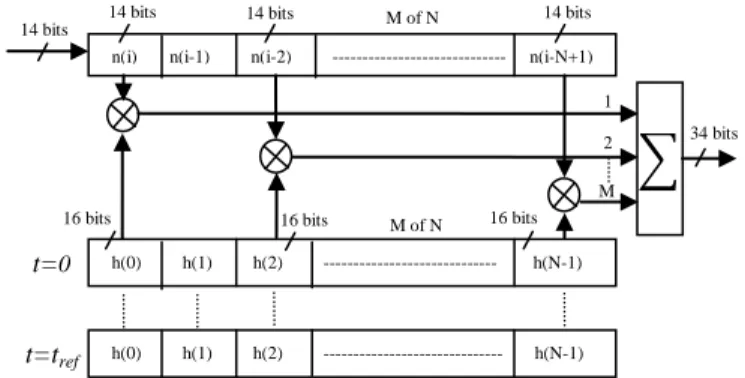
Four FIR filters are considered to simulate 2×2 MIMO channels. The FIR filter length and the number of used multipliers are determined by the taps of each SISO channel.
To use a limited number of multipliers on the FPGA and to switch from one environment to another, a solution is proposed to control the change of delays by connecting each multiplier to the corresponding cells of the shift register and the memory (RAM). Fig. 1 presents one FIR filter of a length
N and with M multipliers (M taps). We have developed our
own FIR filter instead of using Xilinx MAC filter to make it possible to reload the filter coefficients.
Fig. 1. FIR filter N with M multipliers for one SISO channel.
For M = 9 (using TGn model B), the final output is quantified on 34 bits. Due to the use of a 14-bit Digital-to-Analog Converter (DAC), the final output must be truncated. The best solution is the Sliding window Truncation (ST), presented in Fig. 2, which uses the 14 most significant bits.
Fig. 2. Sliding window truncation, from 34 to 14 bits.
To increase the precision of the output signals, an Auto-Scale Factor solution is used [16]. The simulations are made with ISE from Xilinx [2].
IV. IMPLEMENTATION ON FPGA
Fig. 3 shows the XtremeDSP Virtex-IV board from Xilinx [2] used for the implementation of the architecture and the connection between the PCI and the FPGA.
Fig. 3. XtremeDSP Development board Kit-IV for Virtex-IV.
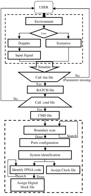
In the recent years, communication usually takes larger place by the use of GUI. In this context, a new algorithm that connects the GUI to the digital block of the FPGA for each configuration is realized. It will be able to implement the considered architecture in a simple way, as shown in Fig. 4. The user configures the parameters, starting by choosing a specific environment (indoor, outdoor, outdoor-to-indoor, etc.), the scenarios, a specific Doppler speed, the considered input signals and the clock frequencies. The user has the possibility
n(i) n(i-1) n(i-2) --- n(i-N+1)
h(0) h(1) h(2) --- h(N-1)
h(0) h(1) h(2) --- h(N-1)
0001010011001100001…
to use an external, internal Gaussian or Dirac input signals. An external or internal clock can be used. The internal clock
provides the Ts of WLAN 802.11 or LTE.
Fig. 4. Implementation algorithm.
In the first stage of the simulation, the system checks the parameters to choose the specific BATCH file (.bat). Then, this batch file calls a new command file (.cmd) specific for these parameters. The command file contains the algorithm that implements the digital block file (.bit) into the FPGA. Moreover, a scan is launched to find a boundary. Then, a configuration of the ports is needed before identifying the used system. In the next step, two processes are made. Firstly, the digital block file (.bit) of the clock is assigned to its position in the boundary. Secondly, a searching task is launched to identify the FPGA code which gives the access to implement the digital block file (.bit) of the required environments parameters in its proper position in the boundary. When the simulation is complete, the output signals are shown on the screen of the oscilloscope, as in Fig. 3.
This solution for MIMO hardware simulators allows, for each configuration, the implementation of different digital block file, which requires multi-task to be applied. It offers simplicity and flexibility for the user to simulate its required parameters. One negative point of this algorithm is the non-acceptable simulation without a batch file [2].
V. RESULTS AND ACCURACY
In order to determine the accuracy of the digital block, a comparison is made between the theoretical and Xilinx output
signals.AninputGaussiansignal x(t)=x1(t)=x2(t) is considered:
where Wt = 384Ts, mx = 3.Wt/4 and σ = mx/32. These
parameters are chosen in a way to show the effect of each path of the impulse responses on the output signals. The ADC and DAC converters have a full scale [-Vm,Vm], with Vm = 1 V.
Thus, we consider xm = Vm/4. The impulse responses can be
presented in baseband with complex values, or as real signals
with limited bandwidth B between fc – B/2 and fc + B/2. In this
paper, to eliminate the complex multiplication and the fc, the
hardware simulation operates between Δ and B + Δ, where Δ = 2 MHz is introduced to prevent spectrum aliasing. To obtain
thespectrumofx(t)between[ , +B],itmustbe multiplied by:
The theoretic output signals are calculated by:
where Mij depends on the number of taps of the channel. We
define the error vector for a 2×2 MIMO system as:
TheRelativeError(RE) is givenforeachoutputsampleby:
and the Relative Signal-to-Noise Ratio (RSNR) by:
SNR = 20
The Global values of the SNR (GSNR) are necessary to evaluate the accuracy. Thus, they are computed by:
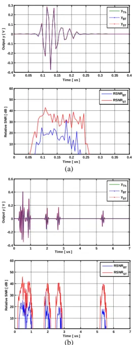
Fig. 5 shows a snapshot of the output signal y1 and the
SNR using TGn B (a) and 3GPP-LTE ETU (b). YTh stands for
theoretical output signal while BT for Brutal Truncation.
Search Search USER Simulate No (Parameter missing) CMD file No Yes Yes Case
Assign Clock file
Assign Digital block file Done Done Search Search System identification Call .bat file Environment Doppler Input Signal Scenarios BATCH file Call .cmd file Boundary scan Ports configuration
(a)
(b)
Fig. 5. Results for y1 using TGn model B (a) and 3GPP-LTE ETU (b).
Table I shows the mean GSNR for each output with the occupation on the FPGA for several environments using standard and measured impulse responses.
TABLE I. MEAN GLOBAL SNR AND OCCUPATION ON FPGA
GSNR (dB) Occupation on FPGA Virtex-IV
Channel y1 y2 Slices (%) RAM (%) DSP (%)
TGn model B 73.3 73.1 14 5 19
TGn model C 73.2 72.3 16 5 30
TGn model D 73.5 73 17 5 38
TGn model E 73.3 73.1 17 5 38
TGn model F 73.4 72.1 17 5 38
LTEmodelETU 72.6 73.2 14 5 19
LTEmodelEVA 73.2 72.9 14 5 19
LTEmodelEPA 73.2 72.2 13 5 15
Measured
Outdoor-to-Indoor 61.7 64.4 21 5 99 Measured
Shipboard 71.4 71.2 20 5 91
The relative error is high only for small values of the output signals because the Gaussian signal test is close to 0.
VI. CONCLUSION
This paper introduced an algorithm based on batch files to configure the FPGA devices. It considers the implementation of the digital block file of the MIMO hardware simulation into the Xilinx Virtex-IV FPGA. This algorithm connects the GUI of the hardware simulator to the digital block on the FPGA. This algorithm allows the user to select the channel parameters that are used to conclude the appropriate digital block file. The objective of this work is to obtain a hardware simulator system for different environments and scenarios. The accuracy and the occupation on FPGA of the architecture for different channel models has been presented and analyzed.
As a perspective, we aim at implementing of high order 8×8 MIMO channels on more performing FPGA as Virtex-VII. Moreover, several measurement campaigns will be carried out to obtain different impulse responses to cover many types of environments.
REFERENCES
[1] A. S. Behbahani, R. Merched, and A. Eltawil, “Optimizations of a MIMO relay network,” IEEE, vol. 56, no. 10, pp. 5062–5073, Oct. 2008. [2] “Xilinx: FPGA, CPLD and EPP solutions and iMPACT User
Guide”,www.xilinx.com.
[3] Wireless Channel Emulator - Spirent Communications, 2006.
[4] Baseband Fading Simulator ABFS - Reduced costs through baseband simulation - Rohde and Schwarz, 1999.
[5] P. Murphy, F. Lou, A. Sabharwal and P. Frantz, “An FPGA based rapid prototyping platform for MIMO systems”, Asilomar Conf. on Signals, Systems and Computers, ACSSC, vol. 1, pp. 900-904, 9-12 Nov. 2003. [6] Agilent Technologies, “Advanced design system – LTE channel model -
R4-070872 3GPP TR 36.803 v0.3.0”, 2008.
[7] V. Erceg, L. Shumacher, P. Kyritsi, et al., “TGn Channel Models”, IEEE 802.11- 03/940r4, May 10, 2004.
[8] H. Farhat, R. Cosquer, G. Grunfelder, L. Le Coq and G. El Zein, “A dual band MIMO channel sounder at 2.2 and 3.5 GHz”, IMTC, Victoria, BC, Canada, May 2008.
[9] P. Almers, E. Bonek et al., “Survery of channel and Radio propagation models for wireless MIMO systems”, EURASIP Journal on Wireless Communications and Networking, Article ID 19070, 2007.
[10] L. Schumacher, K. I. Pedersen and P.E. Mogensen, “From antenna spacings to theoretical capacities – guidelines for simulating MIMO systems”, in Proc. PIMRC Conf., vol. 2, pp. 587-592, Sep. 2002. [11] S. Picol, G. Zaharia, D. Houzet, G. El Zein, "Design of the digital block
of a hardware simulator for MIMO radio channels", IEEE PIMRC, Helsinki, Finland, Sep. 2006.
[12] H. Eslami, S.V. Tran and A.M. Eltawil, "Design and implementation of a scalable channel Emulator for wideband MIMO systems", IEEE Trans. on Vehicular Technology, vol. 58, no. 9, pp. 4698-4708, Nov. 2009. [13] S. Fouladi Fard, A. Alimohammad, B. Cockburn, C. Schlegel, "A single
FPGA filter-based multipath fading emulator", VTC-Fall, Canada, 2009. [14] B. Habib, G. Zaharia, G. El Zein, “Hardware Simulator: Digital Block Design for Time-Varying MIMO Channels with TGn Model B Test”, IEEE ICT, Jounieh, Lebanon, 23-25 April, 2012.
[15] B. Habib, H. Farhat, G. Zaharia, G. El Zein, “MIMO Hardware Simulator with Standard Channel Models and Measurement Data at 2.2 and 3.5 GHz”, Journal of Communication and Computer, 2012. [16] B. Habib, G. Zaharia, G. El Zein, “Accuracy Improvement of MIMO
Hardware Simulator using an Auto-Scale Factor”, International Journal of Research in Wireless Systems (IJRWS), 2013.
0 0.05 0.1 0.15 0.2 0.25 0.3 0.35 0.4 -0.4 -0.3 -0.2 -0.1 0 0.1 0.2 0.3 Time [ us ] O ut pu t y [ V ] yTh yBT yST 0 0.05 0.1 0.15 0.2 0.25 0.3 0.35 0.4 10 20 30 40 50 60 Time [ us ] R e la ti v e S N R [ dB ] RSNRBT RSNRST 0 1 2 3 4 5 6 7 -0.4 -0.2 0 0.2 0.4 0.6 Time [ us ] O ut pu t y [ V ] yTh yBT yST 0 1 2 3 4 5 6 7 10 20 30 40 50 60 Time [ us ] R e la ti v e S N R [ dB ] RSNRBT RSNRST