Université du Québec
Institut National de la Recherche Scientifique Énergie Matériaux Télécommunications
HYDROTHERMAL EPITAXY
OF FUNCTIONAL PEROVSKITE THIN FILMS
parIvan Alejandro Velasco-Davalos
Thèse présentée pour l’obtention du grade de Philosophae Doctor (Ph.D.)
en Sciences de l’énergie et des matériaux
Jury d’évaluation Président du jury et examinateur interne Examinatrice externe Examinateur externe Directeur de recherche
Professeur Fiorenzo Vetrone, INRS - EMT, Canada
Professeure Clara Santato,
École Polytechnique de Montréal Professeur Fabio Variola,
University of Ottawa
Professeur Andreas Ruediger, INRS - EMT
Abstract
1
Abstract
Functional oxides and their thin film epitaxy have become increasingly requested and further improvement in the existing technologies of information storage and energy harvesting heavily depends on the performance of such heterostructures at the nanoscale. Ferroelectric materials show a spontaneous electric polarization, which can be switched repeatedly by applying an external electric field. Since the discovery of ferroelectric BaTiO3 as the first oxide
ferroelectric, the period prior to 1988 was mainly restricted to modelling ferroelectric phase transitions and discovering new ones. However, the focus has been significantly changed in the nineties, when thin films were developed and integrated into semiconductors at the nanoscale. This down scaling and bi-stable polarization of ferroelectrics were attractive in memory devices through ferroelectric random access memory, smart cards etc., and in tunable microwave devices through phase shifters, delay lines, resonators etc., apart from the conventional capacitor applications. Similarly, work on multiferroic can be traced back to pioneering research in the 1950s and 1960s, but there has been a recent resurgence of interest driven by long-term technological aspirations. For more than a decade, BiFeO3, being a magnetic and a strong
ferroelectric material at room temperature, has been renowned as a multiferroic materials that addresses a range of possible applications that no other material class exhibits so far. Out of many possible options, photovoltaic applications are being extensively considered due to the relatively low band-gap (~2.5 eV). These two material systems, BaTiO3 and BiFeO3 are widely considered
as the model systems for ferroelectric and multiferroic properties and hence epitaxial thin film growth on lattice matched SrTiO3 substrates by an inexpensive hydrothermal method are
considered in this thesis.
One of the main requirements of producing high quality epitaxial thin films on SrTiO3
substrates is the single termination of its surface. To this effect, a novel microwave-assisted hydrothermal etching was successfully applied to the surface preparation of pure and Nb-doped SrTiO3 single crystals with (100), (110) and (111) orientations. Without the possibility of fluorine
contaminations from the Teflon liner and by avoiding the etching chemistry involved with HF widely used, the surface structure appears perfect within the limitations of the in-plane and out-of-plane miscut angles. These results indicate that the utilization of this method, without any
Abstract
2 corrosive chemicals during the preparation steps, to achieve atomically flat surface with single chemical termination of SrTiO3 substrates is feasible and compatible with batch processing. This
technique is inexpensive, fast, safe, environmentally benign, compatible with batch processes, and showed remarkable reproducibility. Further, this method does not need an ultra-high vacuum environment and long annealing time at high temperatures. The possibility to reduce the etching time significantly avoids the formation of etch pits and holes on the substrate surface.
The hydrothermal technique is shown to be a feasible way to obtain good crystalline quality thin films of BaTiO3 and BiFeO3. This method is an inexpensive alternative technique, which is
defined as any chemical reaction in presence of aqueous solvents conducted at autogenous pressure, which corresponds to the vapor pressure above room temperature and below the critical point, generally lower than 370 °C for water, in a closed system. As for the synthesis of the thin films, two hydrothermal technique modes were employed; conventional hydrothermal for BaTiO3 and microwave assisted hydrothermal for BiFeO3. The conventional hydrothermal mode,
where the heating process happens by convection at heating rates of 10 °C/min using a stainless steel reactor in a conventional oven; and, the microwave assisted hydrothermal mode, which consists in utilizing a relatively low budget high strength polymer reactor in a microwave oven for which the heating process happens by absorption through water molecules of the 2.45 GHz radiation which allows a more efficient heating process to synthesize films in less time compared to the conventional process.
In the case of BaTiO3 films, TiO2 nanoparticles dispersed in the Ba(OH)2 alkaline solution
are used as precursors. The incorporation of H2O2 into precursor solution served as a strong
oxidant and catalyst for the uniform nucleation of BaTiO3 on the substrate surface. Polarization
reversal in single phase epitaxial and polycrystalline BaTiO3 thin films were demonstrated on
Nb:SrTiO3 and Pt/Al2O3/SiO2/Si substrates, respectively. Raman scattering studies revealed the
necessity of cumulative depositions with 10 min of microwave radiation at a power of 120W for the single phase formation of BaTiO3 films. No traces of impurity phases were present according
to the x-ray diffraction and Raman scattering results which is primarily due to the absence of mineralizers. Local phase hysteresis of BaTiO3 thin film on Nb:SrTiO3 substrate confirms
Abstract
3 Highly ordered BiFeO3 thin films were successfully produced by hydrothermal synthesis
on SrTiO3:Nb (100) substrates. Surfactants were avoided and significantly reduced the
concentration of potassium hydroxide (KOH) by a factor of 10 compared to reports in literature to reduce the leakage current. Due to this reduction of mineralizer, leading to less solubility of the precursors and decreasing the reaction rate, deposition time of ~18 h were required to grow a 40 nm thin film. As-grown BiFeO3 films were also annealed at 500 °C under nitrogen flow for
better crystallization and to remove hydrogen. For the first time, polarization reversal is demonstrated by successful reduction of electronic leakage. A first demonstration of the bulk photovoltaic effect in hydrothermally grown BiFeO3 shows that this technique can be used to
produce multiferroics for photovoltaic applications. Our experimental results confirm realization of single termination of SrTiO3 and epitaxial deposition of BaTiO3 and BiFeO3 by an inexpensive
hydrothermal method with or without microwave radiation.
Keywords: Functional oxides, Perovskites, BaTiO3, BiFeO3, Thin films, Epitaxial growth, SrTiO3, Single crystal, Substrate surface preparation, Etching, Step-terrace structure, Single termination. Hydrothermal synthesis, Atomic Force Microscopy, Ferroelectric polarization switching, Microwave-assisted hydrothermal method, Conventional hydrothermal process, Topography, Bulk photovoltaic effect, Photocurrent.
Acknowledgments
4
Acknowledgments
If I had known that coming to Canada to pursue my PhD would be a complete, sometimes painful, life changing, I would have done it anyways...
First of all, I would like to express my gratitude to my research director Andreas Ruediger for his invaluable pieces of advice, patience, encouragement and criticism in science and in personal life as a great human being that he is. I feel very fortunate to have counted on his mentorship and guidance. I will always have present the first contact email that I had with him. My complete admiration for him.
Thanks to the Institut national de la recherche scientifique, INRS, which provided me the facilities to perform my research. I would also like to thank the jury members, Professors Clara Santato, Fiorenzo Vetrone and Fabio Variola for accepting the invitation and for their helpful contribution.
Special mention goes to Dr. Reji Thomas and Fabian Vargas for their feedback and precious support expressly in the phase of developing and revising my thesis. Nothing would have been the same without them. The astounding good vibe was very inspirational in the research group of Andreas. I feel really pleased to have got along with inspiring colleagues in his research group, and to have had fruitful discussions with them ever since I started this journey. Christian, Mischa, Mathieu, Zabar, Chawki, Julien, Nordine, David, Gitanjali, Mert, Chahinez, Binod, Fernando, Andreas Buescher, Fabian Gersmeier, Thierry, Niklas, Brenda, Angelica, Josefina, Lucia, Manuel, Caroline, Cedric, Azza, and Clarick. There were many people from other groups and institutions who I will always be thankful for their support, friendship, great vibe and love during working hours and at party times: Shun, Maria, Bruno G, Gaston, Maribel, Marta, Eva, Antonio, Shadi, Oscar, Manoj, Belete, Joy, Teresa, Juliana, Mauricio, Bruno M, Denis, Marc, Mernusc, Esen, Maye, Hamid, Stefano, Catalin, Francesca, Romain, Spyros, Jussara, Hassan, Simon, Ania, Pao, Caro, Isabel, and Tim.
I also thank les messieurs Sylvain Gingras, George Lamoureux, and Christophe Chabanier for their technical support, as well to all members of the administration and last but not the least, to professor Federico Rosei whom I appreciate for his great labor to keep the INRS to be one of
Acknowledgments
5 the most recognized institutions in Canada and in the world. I also thank him for allowing me to give me the chance to share great moments with him.
As always, to my parents, Laura and Salvador, who were the first in teaching me pro-feminist/anti-patriarchal values, (specially my mom), for their encouragement, support and endless love; to my sister Lilianita and brothers Josuesin and Vadimcho, my Tita and all my family and friends in Mexico who have been mindful and given moral support and love at every moment. To all my friends in Montreal who also were with me in the good and in the challenging moments and who have had a big spiritual influence. Some of them still in Montreal, others elsewhere, all of them pursuing new and encouraging projects: Lilia, Christelle, Horst, Helga, Andree, Yvan, Isabelle, Didier, Matilida, Samy, Fabien, Emma, Ximena, Mois, Juli, Miguel, Elodie, Oscar, Mcfly, Fercita, Marie, Ghita, Vanesa, Paulita, Berecita, Isaac, Nori, Carol-Anne, Laurie, Matias, Jorge, Hannita, Louison, Celia, Jairo, Margarita, Eve, Ariane, Maribel, Oussama, Emiluna, Salima, Cindy, Jessi, Angelica, Lucia, Luis, Olivita, Julieta, Romina, Etien, Caroline, Sylvie Frida, Pamelita, Renato, Daniela, Chantal Leblanc, Abraham, Lindita, Fernando, Oscar, Gilda, Chantal Latendresse, Florent, Nathalie, Susan, Mape, Candy, Angelika Voor, Helene, Juan Pablo, Marion, Lupita, Mateusz, Caro, Mario, Erandi and Jonathan. Thank you all. You all have a big special place in my heart.
Similar profound thanks goes to professor Carlos Gomez-Yanez who actually was my supervisor in Mexico for my engineer and master’s degree, and with who we kept developing collaboration projects thanks to the financial support from Fonds de recherche du Québec nature et technologies, FRQNT; The Natural sciences and engineering research council of Canada, NSERC; the Canadian institute for photonics innovations, CIPI, support through a PBEEE-MELS fellowship and from Consejo nacional de ciencia y tecnología, CONACyT-Mexico.
Contents 6
Contents
Abstract ... 1 Acknowledgments... 4 Contents ... 6 1. Introduction ... 9 1.1. Multifunctional perovskites ... 101.1.1. Barium titanate (BaTiO3) ... 13
1.1.2. Bismuth ferrite (BiFeO3)... 14
1.2. Thin film epitaxy... 16
1.2.1 Substrate selection ... 19
1.2.2 Substrate surface preparation ... 21
1.2.3 Deposition technique ... 25
1.3 Research objectives ... 27
2. Characterization tools ... 28
2.1. Atomic Force Microscopy ... 28
2.1.1. Piezoresponse Force Microscopy ... 31
2.1.2. Photoconductive Atomic Force Microscopy ... 31
2.2. X-Ray Diffraction ... 32
2.3. X-Ray Photoelectron Spectroscopy ... 32
3. Strontium titanate surface preparation ... 33
3.1. Experimental details... 36
Contents
7
3.3. SrTiO3 (110)... 42
3.4. SrTiO3 (111)... 53
3.5. Conclusion ... 57
4. Multifunctional barium titanate and bismuth ferrite thin films ... 60
4.1. BaTiO3 thin films ... 60
4.1.1 Experimental details... 61
4.1.2. Surface coverage ... 64
4.1.3. Reaction time and cycles ... 66
4.1.4. Epitaxial BaTiO3 on Nb:SrTiO3 substrates ... 68
4.1.5. Ferroelectric properties ... 73
4.2. BiFeO3 thin film ... 74
4.2.1 Experimental details... 75
4.2.2 Morphology and microstructure ... 76
4.2.3 Ferroelectric properties ... 78
4.2.4 Photocurrent ... 79
Contents
8
5. Summary and Outlook ... 84
6. References ... 88
7. Abbreviations ... 96
8. Publications, conference presentations and awards ... 98
Introduction
9
1. Introduction
Multifunctional oxide materials are under continuous investigation and development to sustain the growth of integrated circuit and to improve the energy conversion/storage. Among them, perovskite oxides with ferroelectric and multiferroics properties, play an important role in the current state-of-the-art information storage and processing by realizing new functionalities and advanced electronic devices.1,2 Ferroelectric materials show bi-stable electric polarization which
can be switched by applying an external electric field. This ferroelectric effect was first observed by Valasek in 1921 in the Rochelle salt and it was not considered that time for any practical applications due to the water solubility. However, the ferroelectric switching in BaTiO3 ceramic3
and single crystals4 was discovered later, through systematic dielectric anomaly studies and since
then water insoluble ferroelectric oxide are widely used for many practical applications. However, recent interest in ferroelectric BaTiO3 is in the growth of ultra-thin epitaxial film and strain
engineering with enhanced ferroelectric properties for high density ferroelectric memories and electro-optic devices.5-9 ‘Multiferroic’ is a relatively new term, originally introduced by Schmid,10
which defines a class of materials which exhibit any type of long-range magnetic ordering and ferroelasticity (hysteretic strain), antiferroelectricity and/or ferroelectricity at the same time. However, according to the current usage, ‘multiferroics’ generally excludes the elastic part (most ferroelectrics are also ferroelastic, so that combination is not unusual) and refers only to magnetic and electric properties.11 Since the discovery of enhancement of polarization in heteroepitaxially
constrained thin films of ferroelectromagnetic BiFeO3 at room temperature, multitiferroic BiFeO3
recently ignited interest among materials scientists worldwide and is also attractive for photovoltaic applications.10,12 So oxide materials are an attractive alternative to silicon technology
because they possess multifunctional properties that can be utilized in various novel electronic and energy conversion/storage devices. The ability to realize atomically flat oxide substrates and production of epitaxial heterostructures with multifunctional oxides of atomic layer precision made “oxide electronics” a field of its own and is rival to semiconductors multilayers now. The preparation of conducting and insulating oxide single crystal substrates (SrTiO3) surface with
single termination, the realization of ferroelectric (BaTiO3) and multiferroic (BiFeO3)
Introduction
10
1.1. Multifunctional perovskites
All crystals can be divided into 32 different classes depending on their symmetry; 20 of them exhibit piezoelectricity and among those, 10 are pyroelectric. If the spontaneous polarization of the pyroelectric crystal has two stable states, and this polarization can be switched from one state to the other by the application of an electric field, then the crystal is ferroelectric.13 A
graphical overview of the crystal classification is given in Figure 1.1
Figure 1.1: Classification of the 32 crystal groups; adapted from reference 14.
The dielectric behavior of a non-centrosymmetric crystal which possesses piezoelectric, pyroelectric and ferroelectric properties at the same time is described by:
𝐷𝑖 = 𝜀0(𝜀𝑖𝑗𝐸𝑗+ 𝑑𝑖𝑗𝑘𝑇𝑗𝑘+ 𝑝𝑖∆𝑇 + 𝑃𝑆𝑖) Equation 1.1 where 𝐷𝑖 denotes the electrical displacement in direction 𝑖; 𝜀𝑖𝑗 is the relative permittivity, 𝐸𝑗 the
electric field in direction 𝑗; 𝑑𝑖𝑗𝑘 is the piezoelectric tensor element permitting a crystal to exhibit electric polarity when subject to a mechanical stress 𝑇 and vice versa; 𝑝𝑖 is the pyroelectric coefficient for small temperature changes ∆𝑇 ; and, 𝑃𝑆𝑖 is the inherent spontaneous
polarization20,21. The Figure 1.2a shows a typical ferroelectric P-E hysteresis loop which
represents the polarization reversal by the application of an external electric field. It has been noticed that several authors confuse ferroelectric behavior by reporting unrelated coercive field and remnant polarization from cigar-shaped loops (Figure 1.2b) that are typical of lossy dielectrics2,15.
32 groups
All crystalline materials electrostrictive 11 groups centrosymmetric 21 groups Non-centrosymmetric 1 group Non-piezoelectric 20 groups Piezoelectric 10 groups Non-pyroelectric 10 groups Pyroelectric Non-ferroelectric Ferroelectric
Introduction
11 Figure 1.2: a) Ferroelectric hysteresis loop for a truly ferroelectric material; (b) charge versus voltage giving a cigar-shape loop typical for a lossy dielectric, in this case the peel of a banana; adapted from reference 15.
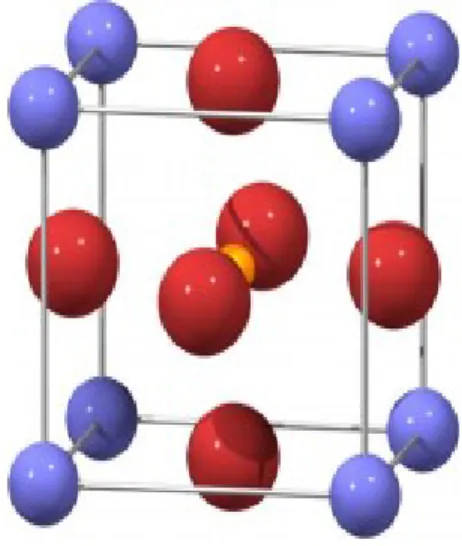
Some materials that exhibit ferroelectric properties belong to the group of so called perovskite structure. The perovskite structure has the general stoichiometry ABO3, where
A cations are located at the corner of the structure, B in the center of the body and O on the face centers as seen in Figure 1.3. The A and B cations can have a variety of charges and in the original perovskite mineral (CaTiO3) the A cation is divalent and the B cation is tetravalent. The
ferroelectric effect is attributed to the dipole interaction between the B body centered cation and the oxygen anion located on the face centers resulting in the B- ionic displacement from the center in non-centrosymmetric structure. This spontaneous ionic displacements or as well named spontaneous polarization can be possible where the force to displace the ion is strong enough to overwhelm the repulsive force between the ions.16
Introduction
12 Figure 1.3: The perovskite structure has the general stoichiometry ABO3, where A atoms are located at the corner of the structure, B in the center of the body and O in the face centers.
On the other hand, multiferroics are formally defined as materials that exhibit more than one primary ferroic order parameter simultaneously in one phase10 as shown in Figure 1.4. In a
ferroic material, polarization 𝑃, magnetization 𝑀, or strain 𝜀 are spontaneously formed to produce ferroelectricity, ferromagnetism or ferroelasticity, respectively.
Figure 1.4:The electric field E, magnetic field H and stress σ control the electric polarization P, magnetization M and strain ε respectively; adapted from reference 17.
Introduction
13 1.1.1. Barium titanate (BaTiO3)
Barium titanate has been considered as a paradigmatic ferroelectric material which possesses a perovskite tetragonal structure at temperatures between 5°C and 120 °C of the type ABO3 as shown in the previous Figure 1.3. The unit cell parameters for the tetragonal phase are:
𝑎 = 0.3992 nm and 𝑐 = 0.4036 nm. The transition from the ferroelectric tetragonal phase to the paraelectric cubic one occurs around 120°C which corresponds to the Curie temperature. At room temperature, BaTiO3 exhibits a polarization along the c axis which is reversible when applying an
electric field. 18-21 The applications of particular interest with this material are positive temperature
coefficient of resistivity (PTCR) thermistors, multilayer ceramic capacitors (MLCCs) and electro-optic devices.2 More recently, ferroelectric properties of BaTiO
3 have been coupled with the
electron tunneling phenomena to develop ferroelectric tunnel junctions which has been subject of investigation.9 Ferroelectric tunnel junctions (FTJ), which are composed of two metal electrodes
separated by an ultrathin ferroelectric barrier, are considered as promising candidates for non-volatile resistive memories. The Figure 1.5 shows atomic force microscopy results of a tunneling heterostructure composed of a metal-ferroelectric-semiconductor configuration (Pt/BaTiO3/Nb:SrTiO3) produced by pulsed laser deposition (PLD), where the height and the width
of the barrier can be electrically modulated as a result of a ferroelectric field effect that leads to a greatly enhanced tunneling electroresistance.9 The author argues that the giant tunneling
electroresistance, reliable switching reproducibility and long data retention observed in this configuration suggest a great potential in non-destructive readout non-volatile memories.
Introduction
14 Figure 1.5: a), morphology of a BaTiO3 surface on Nb:SrTiO3 semiconductor substrates. b), local Piezoresponse Force Microscopy hysteresis loops: top, phase signal; bottom, amplitude signal. c,d, PFM out-of-plane phase and amplitude images recorded after writing an area of 3 × 3 μm2 with −5 V and then the central 1.5 × 1.5 μm2 square with +5 V using a biased conductive tip. e, Current mapping over the same area shown in c),d),e), demonstrating the polarization direction-dependent resistance in the BaTiO3/Nb:SrTiO3 heterostructure. Adapted from reference 9.
1.1.2. Bismuth ferrite (BiFeO3)
Bismuth ferrite is a multiferroic material with polar and magnetic ordering coexisting at room temperature. 28,29 It has a rhombohedral perovskite structure in bulk (monoclinic in thin films)
with bismuth atoms located at the corners of the cell, iron at the center, and oxygen at the face centers.22 It has excellent ferroelectric and piezoelectric properties and it is considered to be a
suitable material for high-temperature applications thanks to its ferroelectric Curie temperature (Tc) ~830 °C and Néel temperature (TN) ~ 370 °C.23 Facing an increasing demand for alternative
Introduction
15 and renewable energy sources, researchers have begun to screen a broader spectrum of photovoltaic materials. Complex oxide compounds can be inexpensive and stable, and their properties can be tuned in order to be applied for photovoltaic applications.24 The low mobility of
charge carriers and the large band gap have so far impeded the use of bulk-photovoltaic materials in solar cells and their use might indeed be in optoelectronic sensor applications instead. The conversion process of light energy to electrical energy in conventional solar cells, e.g. silicon based devices, relies on the charge separation using the potential developed at the p–n junction.25 The
electrons increase the minority carrier density in the p-type region and the holes in the n-type region respectively. The minority excess lowers the potential at the junction, which might be compensated by a current to the electrodes.24,26 In contrast to p-n junctions, photocurrent and
photovoltage in polar materials have been found to arise from the inherent non-centrosymmetry in the bulk material by exhibiting an intrinsic electric field due to their crystal structure. This field can give rise to a charge separation of photo-excited electron-hole pairs. When these charges reach external electrodes, an electrical current is generated. This phenomenon is known as the bulk photovoltaic effect (BPVE).26-28 The main characteristics of this effect are its large,
non-equilibrium photovoltage and its small photocurrent, which is oriented according to the polarization direction and charge-carrier separation in homogeneous media.26,27 The mechanism
by which the anisotropic properties of the dipole excitations can be analyzed is represented by the photovoltaic tensor described in equation 1.2 which expresses the details of the response of the current density 𝐽𝑖 to the light intensity 𝐼, where the components 𝑒𝑘𝑒𝑙∗ represent unit vectors of the light electric field and 𝑖𝑘𝑙 is a third rank complex tensor which expresses the relation of the squares of the incident photon electric fields 𝐸 ∙ 𝐸∗, although this mechanism is not fully
understood29. Nevertheless, polar materials with large bandgap tend to have a fast carrier
recombination having a detrimental effect on the short current, making them unattractive for photovoltaic applications.
𝐽𝑖 = 𝑖𝑘𝑙𝑒𝑘𝑒𝑙∗∙ 𝐼 Equation 1.2
When a ferroelectric in an open circuit is illuminated by ultraviolet light (UV), for example, a high photovoltage, much larger than the band gap, has been observed in the direction of the electric polarization 35,36. The magnitude of this photovoltage is directly proportional to the crystal
Introduction
16 length in the polarization direction. The photovoltaic effect has been studied in ferroelectric BiFeO3 since 2009 when Choi et. al30, reported single ferroelectric domain BiFeO3 crystals
exhibiting a diode-like effect where the forward direction of the diode was determined by the direction of the electric polarization, and the directionality of the diode could be reproducibly switched by large external electric fields. Associated with the diode effect, a substantial zero-bias PV current was induced by visible light. Its relatively small band gap of ~2.74 eV makes it an interesting candidate for high performance photovoltaic and optoelectronic applications26.
1.2. Thin film epitaxy
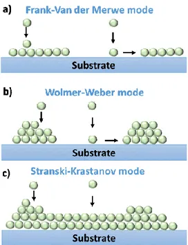
An appropriate understanding of the thin film growth process is required to produce high quality epitaxial thin films on single crystalline substrates. Crystal growth modes (Figure 1.6), as well as the atomistic model to describe the processes for the film growth are discussed in this section. Figure 1.6a corresponds to the layer-by-layer, or Frank-Van der Merwe (FM) growth mode which is observed when atoms are more strongly bounded to the substrate than to each other. When there is no firm bonding between the substrate and the arriving particles, three dimensional island growth can be observed as depicted in Figure 1.6b called Volmer-Weber (VW) mode. Finally, Figure 1.6c describes the layer by layer plus island growth, or Stranski-Krastanov (SK), which is an intermediate mode. After the first or a few monolayers subsequent layer growth is unfavorable and islands are formed on top of this ‘intermediate’ layer.
Introduction
17 Figure 1.6: Film growth modes: a) layer-by-layer Frank-Van der Merwe, b) island Volmer-Weber, (c) Stranski-Krastanov.
The specific growth mode conditions can be understood in terms of surface or interface energy (𝛾), which is the free energy (per unit area) to create an additional surface or interface as shown in Figure 1.7.
Figure 1.7: Schematic representation of the surface energy related to the thin film growth.
Since 𝛾 can be interpreted as a force per unit length of boundary, force equilibrium at a point where substrate and 3D island of the deposited film are in contact requires:
Introduction
18
𝛾𝑆= 𝛾𝐹+ 𝛾𝑆/𝐹𝑐𝑜𝑠Φ Equation 1.3
where 𝛾𝑆 is the surface tension of the substrate, 𝛾𝐹 corresponds to the one of the film, and 𝛾𝑆/𝐹 to that of the substrate/film interface. By employing the Equation 1.3, the (layer-by-layer, FM) and (islanding, VW), can be distinguished by the wetting angle Φ as follows.
FM: 𝛷 = 0, 𝛾𝑆 ≥ 𝛾𝐹+ 𝛾𝑆/𝐹 Equation 1.4
VW: 𝛷 > 0, 𝛾𝑆 < 𝛾𝐹+ 𝛾𝑆/𝐹 Equation 1.5 Stranski-Krastanov (SK) corresponds to a mixed growth mode and it can be explained by assuming that there is a lattice mismatch between the deposited film and the substrate. The lattice of the film tries to adjust to the surface, but at the expense of the elastic deformation energy thus leading to a strained film. The film grows in a layer-by-layer mode until a certain critical thickness and it is when 3D islands are formed31.
The growth modes are a thermodynamic approach to crystal growth. Kinetic effects have to be considered in the hydrothermal process. The individual atomic processes responsible for adsorption and crystal growth on the surface are illustrated by supplies of single atoms (number density n1 (t)) on a substrate with N0 sites per unit area, making the single-atom concentration
n1/N0. These atoms may then diffuse over the surface until they nucleate or re-dissolve, as seen on
Figure 1.8. Atoms or clusters can be captured at defect sites such as steps or nucleate in new 2D or 3D clusters. Each of these processes will be governed by characteristic times, dependent on the single-atom concentration and/or coverage.
Introduction
19 Figure 1.8: Schematic diagram of processes and characteristic energies in nucleation and growth on surfaces, adapted from reference 32
The nucleation density, Nx, of clusters is determined by the amount of particles arriving on
the surface, R (deposition rate) and the distance an atom can travel on a flat surface, the diffusion length.
𝑙𝑑 = √𝐷𝑆𝜏 Equation 1.6
𝜏 is the residence time before re-evaporation or incorporation. 𝐷𝑆 the diffusion coefficient
defined as:
𝐷𝑆 = 𝑣𝑎2𝑒𝑥𝑝 (− 𝐸𝐴
𝐾𝑏𝑇) Equation 1.7
𝐸𝐴 being the activation energy for diffusion, 𝑣 the attempt frequency and 𝑎 the characteristic jump distance. From Equation 1.5 it is clear that the deposition temperature (substrate temperature) is important, influencing the 𝑙𝑑 and with that the nucleation density.32
1.2.1 Substrate selection
A successful realization of an epitaxial growth of thin film on any single crystal substrates requires a thorough consideration to choose the proper single crystal substrate33,34. Figure 1.9
shows the lattice match/or mismatch between some of the single crystal substrates with multiferroic thin films.
Introduction
20 Figure 1.9: Commercially available perovskite substrates to show compatible lattice matching adapted from reference 35
Perovskite strontium titanate, which has a cubic room temperature structure with a = 3.905 Å, is a key player and is widely used as a substrate material for hetero-epitaxy, as well as an active player in various interface controlled phenomena. The selection of SrTiO3 as a
substrate for the hetero-epitaxial growth of multifunctional perovskites was due to (i) its structural compatibility in terms of the lattice matching, (ii) its thermal stability at very high deposition temperatures, and (iii) its chemical robustness in highly reactive or corrosive ambient. Figure 1.10 depicts an epitaxial perovskite heterostructure. Single crystal SrTiO3 can be made electrically
conductive by doping Niobium (Nb) into the lattice in order to create additional energy levels. Doping concentration (0.1 ~ 1 wt. %) change resistivity from 10-1 to 10-3 Ohmcm by partially
substituting Ti4+ by Nb5+, and such substrates are useful for many epitaxial thin film applications,
which require a conducting or semiconducting bottom electrode. Epitaxial perovskite ferroelectrics and multiferroics on semiconducting SrTiO3 substrates have recently proven to be advantageous
for ferroelectric tunnel junctions. Hence, doped SrTiO3 substrates are widely used as bottom
Introduction
21 Figure 1.10: Highly oriented epitaxial perovskite films are of particular interest since its physical properties are directly linked to the direction of the crystallographic orientation. Adapted from reference 36.
1.2.2 Substrate surface preparation
The surface morphology of the substrate is an important aspect to be studied in order to determine and understand the thin film growth. Another important aspect is to procure a best possible interface quality by proper preparation of single chemically terminated surfaces. The (100) oriented SrTiO3 single crystal is non-polar in nature containing a sequence of charge neutral
sheets of SrO and TiO2 along the (100) direction with an interplanar spacing of 𝑎
2. On the other
hand, SrTiO3 oriented in the (110) direction corresponds to a polar surface containing a sequence
of charged sheets of SrTiO4+ and O
24- with an interplanar spacing of 𝑎 2√2.
37 In the case of a (111)
oriented crystal, alternately stacked cationically different (SrO3)4− and Ti4+ charged sheets with
interplanar spacing of 𝑎
2√3 exist. SrTiO3 orientations are discussed in detail in Chapter 3 in terms
of the specific application and method used to prepare them. All the three crystallographic orientations of SrTiO3 are of great importance in achieving heteroepitaxy and multilayer
superlattices of many complex oxides targeted for various applications.38,39 However, most of the
Introduction
22 composition. The step height between them will remain the same after reconstruction and the terrace width is determined according to the equation 1.8 as function of the miscut angle, α which is the angle at which the surface is slanted with respect to the specified crystal plane (0.05 < < 0.3),
tan 𝛼 = 3.905
𝑡𝑒𝑟𝑟𝑎𝑐𝑒 𝑤𝑖𝑑𝑡ℎ Equation 1.8
Surface reconstruction plays an important role that can affect the nucleation mechanisms in thin film growth and may induce different physical properties from those of the bulk40. For
example, according to preparation and ambient conditions, at least 8 different reconstructions and relaxations have been reported for the SrTiO3 (100) surface being ( 1 𝑥 1) one of the most
energetically favorable with TiO2 termination40.
For the SrTiO3 (110) surface under oxidizing conditions, (3 𝑥 1), (4 𝑥 1), (5 𝑥 1) and
(6 𝑥 1) reconstructions have been observed and appear to be related41. A reconstruction on the
(110) surface is termed (𝑛 𝑥 𝑚) indicating that it has dimensions of 𝑛 times the bulk unit-cell length in the (110) direction. These 𝑛 𝑥 1 (𝑛 = 3 − 6) reconstructions show similar features in scanning tunneling microscopy and can evolve from one to the next often with two being present at the same time41.
In the case of (111), the presence of a perpendicular dipole causes the surface energy of the termination to be infinite and the dipole can be removed via four mechanisms: by changing the surface stoichiometry, by redistribution of electrons in the surface region, adsorption of atoms or molecules, and faceting. These mechanisms allow a large number of reconstructions to be formed, with variable compositions and surface chemistry. It has been found that when polished and unsputtered SrTiO3 (111) samples are annealed in ultrahigh vacuum (UHV) at 850 °C for 30 min,
a surface with coexisting domains of (√7 𝑥 √7) R19.1° and (√13 𝑥 √13) R13.9° reconstructions are formed42. Few other reconstructions on (111) have been reported; for example, a Ti4+-rich
(4 𝑥 4) reconstruction by annealing in UHV at 1200 °C for 5 min and studied the influence of using different atmospheres finding that annealing in O2 the surface was more Ti enriched than
Introduction
23 In order to get uniform substrate/film interfaces, the substrate surface should be single chemically terminated, i.e. it should be either SrO or TiO2 for (100), (SrTiO) or (O2) for (110) and
(SrO3) or Ti for (111) orientations.The practical importance of obtaining this step-terrace on the
surface, which is unavoidable when the single crystals are cut and polished at some controlled ‘miscut’ angle, a few fractions of a degree off with respect to the nominal orientation of the crystal lattice, are very important in realizing epitaxy as steps often act as nucleation sites during the film growth. Control of this step density and knowing the surface prior to deposition is important to obtain reproducible epitaxy under identical experimental conditions. Thus surface step morphology is used as a parameter to optimize subsequent thin film growth.43 It is essential to
carefully control the substrate surface to control the nucleation and improve the quality of thin films.
The most common procedure to obtain atomically flat step-and-terrace structures with single chemical termination is by immersion of the SrTiO3 substrate in a buffered hydrofluoric
(HF) solution followed by an O2 annealing at elevated temperatures.44,45 Not only does the HF
treatment impose severe safety precautions, it is also environmentally hazardous. It has been shown that HF etching promotes incorporation of F within the top layers of TiO2 (an average of
~ 13 % of the O anions are replaced by F) which results in lower electron mobility at complex oxide hetero-junctions due to impurity scattering.46 This fluorine contamination can be avoided by
replacing HF with boiling DI H2O and optimizing the time-temperature product of the annealing
step, respectively.39 An approach that substantially reduces the processing time and achieves
surfaces of equal quality as under buffered HF treatment without the possibility of fluorine contamination is of outmost importance and hence a novel a novel approach is necessary. Since SrO is a basic oxide (metal oxidation state < +4, forms a base with water) and TiO
2 is an acidic
oxide (metal oxidation state > +4; forms an acid with water), the control of the pH of the wet etch
solution provokes either SrO or TiO2 termination.44 Water adsorption and dissociation studied by
density functional theory supported the experimentally observed selective hydroxylation of the SrO-termination in the regime of low water partial pressures.47 This Sr-hydroxide complex
improves the solubility of SrO layer under hydrothermal conditions compared to the TiO2 layer.
Introduction
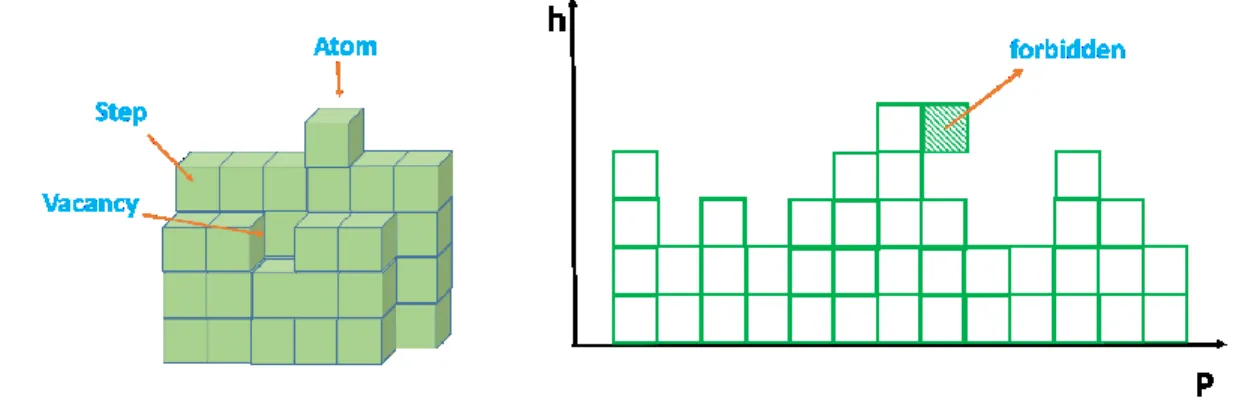
24 The simplest way to approach the problem of surface roughening is to consider the surface of a Kossel crystal, which leads to the so-called TSK (Terrace, Step, and Kink) model for the surface (Figure 1.11). The crystal is made by piling together cubic unit cells which interact through their lateral faces with an energy. The ground state of a crystal surface is obtained when the cubes form a close-packed arrangement with every square face lying in the same plane. When the temperature is raised, thermal excitations can appear. These are point defects: adatoms, forbidden vacancies and kinks on steps or collective defects forming steps which can eventually isolate closed flat domains. All of these defects lead to what we shall call atomic roughness.
Figure 1.11: Kossel crystal (left) and Solid on solid (SOS) model (right).
In order to characterize this roughness more quantitatively, we shall restrict the model somewhat using the SOS assumption (Solid-On-Solid). As far as vacuum/solid interfaces are concerned, this hypothesis is generally quite well verified. Then any surface configuration can be characterized by a set of integers which represents the height of columns above the reference plane.32 The surface morphology and the dynamics of growth after the formation of interfaces and
surfaces can be described in microscopic detail through discrete growth models. In the ballistic deposition model (BD), the particles rain down vertically onto a d’-dimensional substrate and aggregate upon first contact. It uses simple basic laws to determine these surface characteristics on a lattice (Figure 1.12) by generating a non-equilibrium interface that exemplifies many of the essential properties of a growth process.
Introduction
25 Figure 1.12: The ballistic model (BD) with the nearest-neighbor, illustrating two sticking possibilities for the newly deposited particles.
A particle is released from a randomly chosen position above the surface, located at a distance larger than the maximum height of the interface. The particle follows a straight vertical trajectory until it reaches the surface whereupon it sticks. The deposited particles form a cluster or an aggregate with a very particular geometry. In this work we use the height to height correlation function (HHCF) to quantify the roughness.
1.2.3 Deposition technique
The hydrothermal method can be effectively used for the surface preparation of SrTiO3
single crystals and for the thin film deposition of BaTiO3 and BiFeO3 multiferroic materials.
Epitaxial thin films of BaTiO3 and BiFeO3 are typically produced by means of physical methods
such as radio frequency sputtering, pulsed laser deposition (PLD) or molecular beam epitaxy (MBE); and chemical techniques such as chemical vapor deposition (CVD), sol-gel, atomic layer deposition (ALD) or hydrothermal processes.2,48,49 Most of these methods require relatively
expensive setups, as well as high temperature processes, except for the sol-gel, ALD and the hydrothermal method which correspond to low energy processes. As reported in literature, sol-gel depends upon a subsequent annealing step to achieve the necessary crystallinity, whereas in the case of ALD, which certainly provides a crystallinity to the product, a thermal treatment could be required to enhance it. The use of the term “hydrothermal” was initiated in the middle of 19th
Introduction
26 create changes in the earth’s crust leading to the formation of various minerals.50 The hydrothermal
method is considered as a mild and low temperature process. It is defined as any chemical reaction in presence of aqueous solvents conducted at autogenous pressure in a closed system. This pressure (> 1 atm.) is generated by the vapor pressure above room temperature and below the critical point (25 °C < T < 370 °C, in the case of water). The use of mineralizers could be required to promote the solubility.51-53 This technique has gained interest among researchers because of an increase of
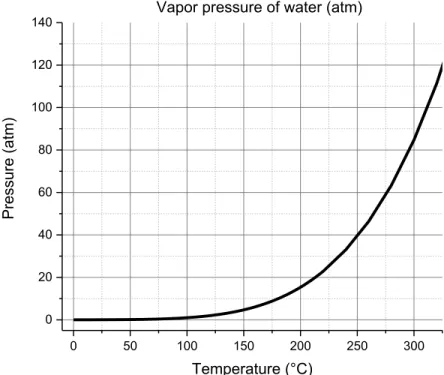
the development of new materials, primarily ceramic oxides that can be prepared under mild conditions. The Figure 1.13 shows the vapor pressure diagram of water as function of temperature. When getting close to the critical point of water, at approximately 374 °C, the dielectric constant of water decreases dramatically, thus water can act as organic solvent.
Figure 1.13: Vapor pressure diagram of water as function of temperature.
More recently, the addition of microwave energy into hydrothermal process has added the convenience of producing thin films and nanostructures with comparable improvement in crystallinity with respect to a conventional hydrothermal process while requiring significantly less time and reducing the cost of energy by about thousands of times54,55. Metallic surfaces are good
reflectors of microwaves; however, electrically semi-conductive materials as Nb doped SrTiO3
0 50 100 150 200 250 300 0 20 40 60 80 100 120
140 Vapor pressure of water (atm)
Pressure (atm)
Introduction
27 allow microwave to pass through them with very little absorption and thus, the heating effect directly depends on the microwave radiation on water.
1.3 Research objectives
BaTiO3 and BiFeO3 are the model perovskite oxide systems that exhibits ferroelectric and
multiferroic properties, respectively. Epitaxial thin films of ferroelectric BaTiO3 and multiferroic
BiFeO3 are very interesting for the non-destructive readout non-volatile memories and
photovoltaic applications, respectively. A successful realization of an epitaxially growth thin film requires a proper single crystal substrate. Single crystal SrTiO3 is widely used as a substrate
material for hetero-epitaxy, as well as an active player in various interface controlled phenomena. In order to get a uniform epitaxial interface between the substrate and the film, the SrTiO3 surface
should be single chemically terminated prior to the film deposition, i.e. it should be either SrO or TiO2 for the (100); SrTiO4+ or O24- for the (110); and SrO34- or Ti4+ for the (111) crystallographic
orientations. The main goal of this research is to investigate the realization of pure and Nb doped SrTiO3 substrate surface with single chemical termination; and to address challenges in fabricating
BaTiO3 and BiFeO3 thin films on single chemically terminated Nb:SrTiO3(100) substrates with
low electric leakage which might be influenced by the hydrogen from the hydrothermal process or by impurities coming from mineralizers. The use of hydrogen peroxide as a strong oxidizer (hydrogen scavenger) is also discussed.
The specific objectives of the thesis are:
Preparation of single chemically terminated pure and Nb doped SrTiO3 substrate surface
with a novel, fast and environmentally benign hydrothermal etching method.
Synthesis of BaTiO3 and BiFeO3 thin films by conventional and microwave assisted
hydrothermal methods
Characterization of the substrate surface with atomic force microscopy and x-ray photoelectron spectroscopy.
Study the structure, microstructure and ferroelectric properties of BaTiO3 and BiFeO3
Characterization tools
28
2. Characterization tools
The work presented in the thesis consist of single chemically terminated surface preparation of pure and Nb doped SrTiO3 substrates by a microwave assisted hydrothermal
method. Similarly, thin film preparation of BaTiO3 and BiFeO3 multifunctional oxides on
Nb:SrTiO3 were also realized by a microwave assisted and conventional hydrothermal technique.
The experimental details of the hydrothermal method used for the surface preparation and thin film deposition are discussed in chapter 3 and 4, respectively. The different orientations of SrTiO3
surfaces and properties of multifunctional oxides were characterized with various tools and that are discussed here.
2.1. Atomic Force Microscopy
Atomic Force Microscopy (AFM) is a technique that allows to obtain topographic images by using a sharp tip at the end of a cantilever that is scanned over a surface.14 The AFM is equipped
with piezoelectric crystals that control the movement of the tip relative to the sample. The cantilever acts as an optical lever arm reflecting a laser beam onto a four sector photodiode which measures the deflection of the beam and thereby the deformation of the cantilever in interaction with the surface (Figure 2.1). The measured deflection gives a topography image of the sample to estimate the thickness of a film by doing a line profile of the cross section between an edge of the film and the substrate. Depending on the type of sample, the probe and/or set up experiment, ferroelectric or photoconductive measurements can be also determined as explained in 2.1.1 and 2.1.2 of the present document.
Characterization tools
29 Figure 2.1: Principle of Atomic Force Microscopy. The cantilever reflects a laser beam, and the movement is detected by a four sector diode.
The principle of atomic force microscopy is the atomic interaction of the tip with the surface of the material in question. Figure 2.2 shows the Lennard-Jones potential in which at very small tip-sample distances (a few angstroms) a very strong repulsive force appears between the tip and sample atoms due to the overlap of the electronic orbitals at atomic distances. When this repulsive force is predominant, the tip and sample are considered to be in “contact”. An instantaneous polarization of an atom induces a polarization in nearby atoms and therefore an attractive interaction due to Van der Waals forces.
Characterization tools
30 Figure 2.2: Atomic interaction at different tip-surface distances.
AFM images can be obtained by two main regimes: The contact mode where the deflection of the cantilever is maintained constant, and the non-contact regime where the tip is oscillated at the resonance frequency and the amplitude of the oscillation is maintained constant. A combination of these two modes leads to a semi-contact or tapping mode where only intermittent touching occurs on the sample. Hence, the dragging forces during scanning are greatly reduced leading to less damage of the sample. During oscillation, the tip goes through both the attractive and the repulsive regimes of the tip-sample force field and it provides a higher resolution. In the present work we kept the focus on the semi-contact mode, except for the case of photovoltaic measurements where contact mode was employed.
In the semi-contact mode, three different images are obtained simultaneously. One that corresponds to the topography, the second one to the phase image which depicts the phase lag between the signal that drives the cantilever to oscillate by a piezoelectric driver, and the cantilever oscillation output signal. In phase image, a contrast can be interpreted by variations in surface properties as adhesion 14; and an error signal image. The morphological analysis of the substrate
surface and the thin film was carried out using atomic force microscopy (AFM, Smart SPM1000-AIST-NT Inc.) and silicon probes (Nanosensors, PPP-NCHR).
Characterization tools
31 2.1.1. Piezoresponse Force Microscopy
Piezoresponse Force Microscopy (PFM) is a tool that has been extensively employed to characterize materials in the nanometer scale allowing to evaluate the ferroelectric properties by the inverse piezoelectric effect.14 Ferroelectric properties of the films were investigated by means
of a PFM module coupled to the AFM system (AFM, Smart SPM1000-AIST-NT Inc.) by using a soft conductive probe (HQ:NSC15/Pt-MikroMasch) as top electrode and a semi-contact technique called Top-PFM developed by AIST, where the probe is gently “scanned” over the sample surface in the semi-contact mode, applying an AC signal only when the tip is in “touch” with the sample generating an electric field under the tip which excites the ferroelectric domains locally due to the inverse piezoelectric effect. Top-PFM technique limits damage to both the sample and the probe by avoiding friction force. The piezoelectric response of the material leads to a mechanical movement of the cantilever and, taking into account the configuration previously shown in Figure 2.1, the laser will be reflected and detected by the photodiode.
2.1.2. Photoconductive Atomic Force Microscopy
In order to study the photovoltaic properties for the case of BiFeO3, photoconductive
atomic force microscopy (PCAFM) was conducted using a conductive probe (HQ:NSC15/Pt-MikroMasch) in contact mode by illuminating the sample locally with a UV laser (355 nm) in order to read the photo-generated currents by the short circuit current (when the voltage is zero). The setup is shown in Figure 2.3.
Characterization tools
32 Figure 2.3: Setup for photovoltaic characterization (PCAFM); adapted from reference 56.
2.2. X-Ray Diffraction
Crystalline properties of the film were measured utilizing X-ray diffraction (XRD, Panalytical Xpert Pro, Cu K radiation) in -2 mode and epitaxial character can be evaluated by
means of scan mode. The crystallite size was calculated using Scherrer equation and lattice parameter out-of-plane was determined using the Nelson Riley extrapolation function.57
2.3. X-Ray Photoelectron Spectroscopy
X-ray photoelectron spectroscopy (XPS) is a very surface sensitive characterization tool which provides valuable quantitative and chemical state information from the variations in binding energies, or chemical shifts within a depth of 3 to 10 nm, and the identification of the elements in the sample can be made directly from the kinetic energies of the ejected photoelectrons:
𝐸𝐾 = ℎ𝑣 − 𝐸𝐵− 𝜙 Equation 2.9
where 𝐸𝐾 corresponds to the kinetic energy of ejected photoelectron, 𝜙 the spectrometer work
Strontium titanate surface preparation
33
3. Strontium titanate surface preparation
This chapter discusses the existence of different chemical terminations on single crystal strontium titanate (SrTiO3) substrates and to realize single chemical termination on its surface to
address epitaxial oxide thin film growth with uniform interface. In the case (100) oriented SrTiO3,
alternating layers of (SrO) and (TiO2)are separated by d100/2 (a/2=0.2 nm) existing along <100>
direction and equivalent (SrO) or (TiO2) stacks separated by d100 (a/1=0.3905 nm), where ‘a’ is
the lattice constant (0.3905 nm) of SrTiO3. Similarly, in the case of (111) orientation alternately
stacked layers (SrO3)4− and Ti4+ separated by d110/2 (a/23=0.113 nm) exist along <111> direction)
and the equivalent (SrO3)4− or Ti4+stacks separated by d111 (a/3=0.225nm). In both (100) and
(111) orientations, two adjacent layers contains either Sr or Ti only, even though the composition of the layers (in terms of O coordination) is different. However, in the case of (110) orientation, equivalent stacks are separated by d110 (a/2=0.276nm) and adjacent (SrTiO)4+- (O2)4− stacks
separated by d110/2 (0.138 nm); suggesting both Sr and Ti exist together in one of the adjacent
layers. In terms of polarity of the surface (110) and (111) are similar as they are charged polar surface, whereas (100) is a neutral surface. The aforementioned layers are restricted to the out-of-plane direction, i.e. direction perpendicular surface. The in-out-of-plane layers are discussed now as it concerns the morphology of surface, very important for the thin film deposition. In ideal cases, when the miscut angle is zero, which is the angle at which the surface is slanted with respect to the specified crystal plane, the cleaved single crystal surface is terminated with one of the layers and hence it will be always single chemically terminated allowing a uniform epitaxial interface. However, the substrate miscut is unavoidable when a single crystal is cut for a particular orientation and polished, with the macroscopic top surface misoriented (in-plane as well as out-of-plane) with respect to the closest low index (hkl) plane.59 So in real case, single crystal substrate
surfaces are composed of step-terrace features as can be seen in Figure 3.1. For a surface with terraces of average width L and separated by steps of height H, the out-of-plane miscut angle (so-called: miscut angle,) is defined as = atan(H/L) and the in-plane miscut angle (so-(so-called: miscut direction, ) is defined azimuth angle of the step with respect to the closest crystal direction with lower step energy, which are schematically shown in Figure 3.1.59 H is the multiple of
Strontium titanate surface preparation
34 or the similarity of the chemical composition of two adjacent terraces and in short the surface termination in general as discussed below.
Figure 3.1: Sketch of a miscut substrate. (a) L, H and are the terrace width, step height, and miscut angle respectively. (b) Sketch of a vicinal surface where the steps present an overall in-plane misorientation with respect to the main crystallographic direction parallel to “a” axis. Adapted from reference 59.
SrTiO3 substrates with low miscut angle (0.05 < < 0.3) corresponding to terrace widths in the
70–500 nm) are available. As we know, one of the prerequisites for high quality epitaxial thin film growth on SrTiO3 substrate with uniform interfacial properties is the realization of
single-termination and atomically flat surfaces. As-received low miscut angle SrTiO3 substrates from the
vendor consist of mixed termination and are characterized with dhkl/2 step height between adjacent
terraces (or odd multiple of dhkl/2). A step height of a, a/2 and a/3 (or multiples of them) for
(100), (110) and (111), respectively, ensure single termination on the surface.
Figure 3.2 depicts the three different crystallographic orientations of SrTiO3, (100), (110)
and (111) with interplanar spacing of a, a/√2, and a/√3 corresponding to single termination for the two different chemical terminations.
Strontium titanate surface preparation
35 Figure 3.2: Depicts the three different crystallographic orientation of SrTiO3, [100]. [110] and [111] with interplanar spacing of a, a/√2, and a/√3, where a = 0.3905 nm.
Out of the three aforementioned surfaces, the orientations that allow selective chemical etching to realize single termination are [100] and [111] due to the fact that each alternate layer contains either Sr or Ti compounds. In contrast, SrTiO3 (110) contains (SrTiO)4+ and (O2)4− stacks
normal to the (110) plane, and hence preferential etching may not serve the purpose in comparison to the (100) and (111) surfaces. This chapter discusses a novel route for the preparation of such
Strontium titanate surface preparation
36 surfaces on pure and Nb doped SrTiO3 substrates of all three orientations. The preparation consists
of a two-step process: a chemical etching followed by an annealing in O2 atmosphere which
minimize reduction and the atomic arrangement for thermodynamic equilibrium on the surface and the step edge can be uniform.
3.1. Experimental details
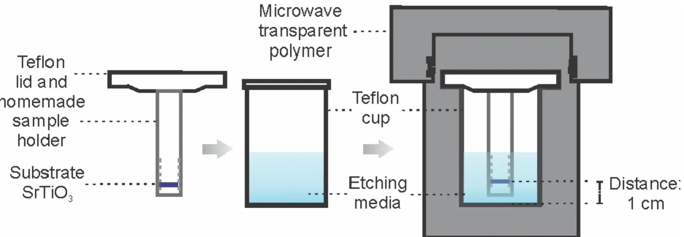
A microwave assisted hydrothermal etching technique was adopted for the surface preparation as a safer and less expensive alternative to the standard procedure that consisted in the immersion of the substrate in a buffered-HF44. The schematic diagram of the microwave
compatible hydrothermal reactor used for the SrTiO3 substrate etching is shown in Figure 3.3. It
consist of a polytetrafluoroethylene (PTFE) cup (from Parr Instrument) which is the container for the etching medium and a home built substrate holder (custom designed for holding multiple substrates) which is attached to the lid of the aforementioned cup. This substrate holder/etchant cup assembly ensured stable positioning of the substrate at one specific distance from the bottom of the cup during the entire hydrothermal processing. One side polished pure and Nb (0.5 wt. %) doped SrTiO3 single crystal substrates (5 × 5 × 0.5 mm, miscut angle < 0.3° from Crystec GmbH)
were used. Both, neutral (deionized water, pH 7) and basic (10% ammonium hydroxide (Sigma-Aldrich >99.99%) solution, pH 10), conditions were used. Substrates were kept inside the PTFE cup at a distance of 1 cm from the bottom with the polished side facing down. This face down positioning reduces particle contamination and re-adsorption on the surface. The Teflon O-ring attached to the cup cover develops and maintains a tight seal without heavy pre-loading. This sealed cup/substrate assembly was then housed into a polymer autoclave (microwave digestion bomb from Parr Instrument: Model 4781) to ensure overpressure while heating the solution with microwave energy. The temperature and pressure generated within a microwave bomb are solely depended upon the filling level, time of exposure and the power level. In the present case, the volume fill factor of the etching media was fixed at 66% of the total volume of the cup. The microwave oven used for the heating was a commercial kitchen microwave (Panasonic Inverter) which provides a continuous microwave irradiation (non-duty-cycle). Duty cycling the power ON and OFF is a common low cost method in most of commercial microwave ovens in which the power level is always at maximum power during the ON time60. The average power level is based
Strontium titanate surface preparation
37 on the amount of ON time vs. OFF time and this power control is not good in the case of the hydrothermal process since, as shown in Figure 1.13, small changes in temperature would represent a big variation in the pressure and the process would not be uniform. The vessel is always placed in the center of the rotating plate with an output power level was fixed at 360 W and time of microwave exposure was 3 and 4 minutes, respectively, for the ammonium hydroxide solution and for DI water (Resistance > 10 MΩ) media. The reactor was kept in the microwave oven after the heating cycle for a period to allow the internal pressure to drop significantly and to then submerge the lower part of the reactor in water to accelerate cooling down to room temperature.
Figure 3.3: Experimental setup showing a cross-section of the microwave-compatible hydrothermal reactor.
Eventually the etched substrates were annealed at 1000C-1100C for various time in a programmable tube furnace (from MTI Corporation) under oxygen flow of 80 sccm and allowed furnace cooling to room temperature. The topography of the substrate was then analyzed by Atomic Force Microscopy, AFM (Smart SPM1000-AIST-NT Inc.) in tapping mode. Silicon cantilever tips (Model PPP-NCHR from NANOSENSORS) with typical tip radius < 8 nm, length 125 m and tip height 10-15 m have been used. Sr and Ti contents on the substrate surface were determined with X-ray photo-electron spectroscopy (VG Escalab 220i XL) using Al K
(1486.6 eV) radiation from a monochromatic x-ray source operating at 400 W. Spectra were calibrated using carbon by assigning the binding energy of 284.6 eV to the C1s peak position to
Strontium titanate surface preparation
38 compensate for a possible shift in the peak position due to charging effects.61 Commercially
available (100, 110 and 111) oriented SrTiO3, pure and 0.5 % wt. Nb doped SrTiO3 single crystal
substrates of 5 x 5 x 0.5 mm, (CrysTec GmbH, miscut angle < 0.3°) were used for the present study.
3.2. SrTiO3 (100)
SrTiO3 with the crystallographic direction (100) is widely used as a substrate for the
heteroepitaxial growth of high TC superconductors62, colossal magneto-resistance manganites63,
multiferroics64,65 and other complex perovskite oxides66,67. Recent discoveries of various
electronic properties35,68,69, 2D electron gas (2DEG)70, superconductivity71, ferromagnetism and
magnetoelectric effects at the interface of complex oxides72,73 stimulated additional research in this
field. One of the procedures to obtain atomically flat step-and-terrace structures with single chemical termination is by immersion of the SrTiO3 substrate in a buffered hydrofluoric (HF)
solution to selectively remove one chemical termination, followed by an O2 annealing at elevated
temperatures to obtain a sharp well-arranged single chemically terminated surface.44,45 Another
method avoids this fluorine contamination by replacing HF with boiling DI H2O and optimizing
the time-temperature product of the annealing step.39 Ohnishi et al.74 have reported an enrichment
in Sr close to the surface layer upon heating to 1000K in air by means of electron spectroscopy resulting in a possible partial coverage of the surface with SrO. Direct investigations of the (100) surface by atomic force microscopy75 however revealed that even at 1600K, the surface had to be
exposed for 12 to air in order to achieve a partial SrO termination and 72h for a complete SrO termination.
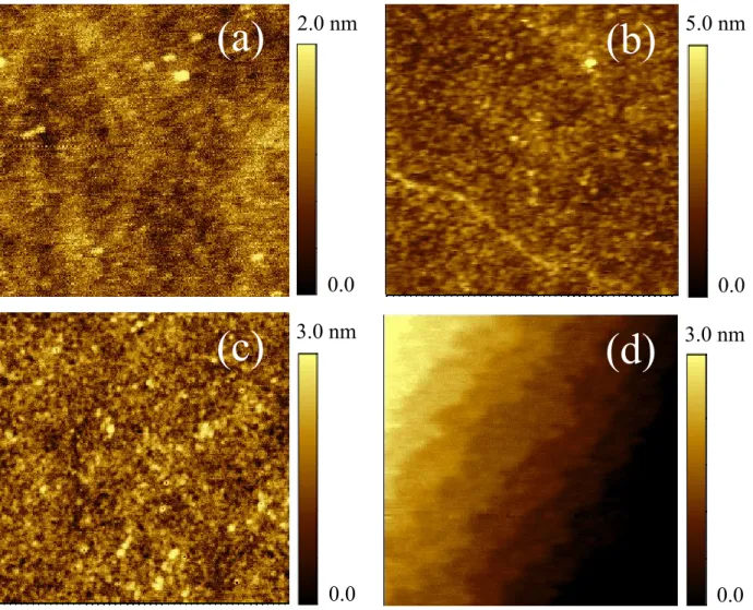
Figure 3.4 depicts the evolution of surface morphology as revealed by the AFM of the undoped SrTiO3 (100) single crystal substrate at different stages of the microwave-induced
hydrothermal etching and annealing processes. As can be seen from Figure 3.4a, the sample surface of the as-received substrate is featureless due to physisorbed contamination. Figure 3.4b depicts the surface topography of the substrate after the hydrothermal etching. Terraces with 3.90 ± 0.1 Å in height, corresponding to one unit cell within experimental errors, are observed. For the aforementioned reasons, we presume that the given conditions strongly favour a TiO2 termination.
Strontium titanate surface preparation
39 Figure 3.4c illustrates the AFM surface topography of the substrate, which undergoes microwave-induced hydrothermal etching in water for 3 min followed by the oxygen annealing at 1000°C for 10 min. As can be seen from this subfigure, the topography shows a clear step-terrace structure with sharp steps of 3.90 ± 0.1 Å in height and smooth step edges. Additionally, the phase image of the same scan of the topography shows uniform contrast, and hence confirms one chemical termination (Figure 3.4d).
Figure 3.4: (a) SrTiO3 (100) single crystal substrate as-received; (b) hydrothermally etched in water; (c) hydrothermally etched in water followed by an annealing step, and (d) its corresponding phase image depicting single chemical termination.
We further extended this preparation procedure to niobium doped (0.5 wt. %) SrTiO3 (100)
substrates as well. This metallic/semiconducting substrate is of substantial technological interest as conducting bottom electrode for many applications and in itself still subject of intense
Strontium titanate surface preparation
40 research.76 Figure 3.5 depicts the evolution of the surface topography of SrTiO
3:Nb (100)
substrates at various stages of the surface preparation processes obtained by means of AFM in tapping mode. As can be seen from Figure 3.5a, for the as-received sample, no surface features are detectable, similar to the undoped SrTiO3 (Figure 3.4a) surface. Figure 3.5b shows the substrate
surface after etching alone, and the result is again similar to the undoped SrTiO3 (Figure 3.4b) with
a step height of approximately 0.4 nm. Finally, Figure 3.5c, which corresponds to the substrate surface that was hydrothermally etched in water and subsequently annealed, shows the final result, a step height of 4.0 Å ± 0.1 and smooth terrace edges. The slight increase in the step height compared to the undoped SrTiO3, is attributed to an increment of the lattice parameter upon
niobium doping. The AFM phase image (Figure 3.5d) of the same scan shows uniform contrast, which independently confirms single termination. Undoped and niobium-doped SrTiO3 (100)
Strontium titanate surface preparation
41 Figure 3.5: (a) SrTiO3:Nb (0.5 wt. %) (100) as-received; (b) hydrothermally etched in water only; (c) hydrothermally etched in water after thermal treatment and (d) its corresponding phase image depicting single termination.
For comparison, a SrTiO3:Nb (0.5 wt. %) (100) single crystal substrate was also processed
in boiling water following the recipe of Chambers, et al46. However, instead of using 30 min as
they suggested, we used 3 min for direct comparison with the microwave-induced hydrothermal etching in order to see the effect of processing time on the surface evolution. In this case, the observed step height was 2.0 Å ± 0.1, which corresponds to half a unit cell, indicating incomplete etching. This comparative study shows the effectiveness of microwave treatment in water through a substantially reduced etching time thus making the SrTiO3 substrate cleaning process faster.