University of Quebec
Institut national de la recherche scientifique Centre Énergie, Matériaux et Télécommunications
Oxide Perovskites for Solar Energy Conversion
byJoyprokash Chakrabartty
Dissertation submitted for the partial fulfillment of the requirements of the degree, Doctor of philosophy, Ph.D.
in science of energy and materials
Jury d’évaluation
Research supervisor Federico Rosei,
Professor and Director, INRS-EMT. Research co-supervisor Riad Nechache,
Principal Investigator, École de Technologie Supérieure (ETS), Montréal.
Internal examiner and Mohamed Chaker, the president of the Jury Professor, INRS-EMT. External examiner Nazir P. Kherani,
Professor, University of Toronto. External examiner Jerome Claverie,
Professor, University of Sherbrooke.
Abstract
Inorganic ABO3 perovskite materials exhibit exotic physical and chemical properties due to their
exceptional crystal structures and thus offer exciting opportunities for spintronics, computer memories, sensors, microwave and photovoltaic (PV) device applications. Since the discovery of bulk photovoltaic (BPV) effect in non-centrosymmetric crystals, the perovskite oxides including BaTiO3 (BTO), LiNbO3 (LNO), BiFeO3 (BFO), BiMnO3 (BMO), and Pb(Zr,Ti)O3 (PZT) drew
enormous interest in fundamental science research, as they exhibit either a suitable band gap or larger than band gap photovoltages (up to 1000 V) under homogeneous light illumination. However, owing to their insulating characteristics retain even at the dimensions down to nanometer scale, the charge carrier conduction in polar perovskites is extremely poor resulting in the generation of low photocurrent density, typically in the µA/cm2 range and below. Driven by
the challenges of improving photocurrent density, in this project, we have investigated BMO and BFO compounds in view of their integration as active materials in PV devices in order to improve the photocurrent density and thus solar power conversion efficiency (PCE). BMO in thin film form possesses ferroelectric behavior i.e. a remnant polarization of ~6 µC/cm2 at room temperature and
its low band gap value (~1.2 eV) efficiently absorbs light wavelengths exceeding the visible wavelengths of the solar spectrum. In contrast, BFO thin films exhibit strong ferroelectricity with a remnant polarization of ~ 55 µC/cm2 and a band gap of ~2.7 eV that corresponds to visible light
of solar spectrum. Although the physical and chemical properties of various forms of BFO, from bulk to nanoparticles are widely investigated in solar cells, the potential of BMO alone or in combination with other perovskites is rarely investigated and reported so far in the field of solar energy conversion.
In the first part of this thesis, we demonstrate a bilayer-stacking scheme, more specifically a heterostructure based on BFO/BMO epitaxial bilayer thin films grown by pulsed laser deposition (PLD) onto Niobium doped (111)-oriented SrTiO3 (STO) substrates. The BFO/BMO bilayers as
photoactive materials in solid-state PV devices show remarkable PCEs up to 1.43% under 1 sun solar radiation (AM 1.5G), which is higher than those reported values for individual BFO or BMO thin films. The fill factor (FF) is determined to be 0.72 which is a remarkable value for ferroelectric perovskite-based devices. The bilayers exhibit prominent ferroelectric behavior (~100 µC/cm2)
compared to individual BFO or BMO films. To describe the PV responses, we use a traditional interfacial model where an interface generated electric field is significantly modulated by spontaneous polarization of the materials.
In the second part, we demonstrate a PV device based on Bi-Mn-O composite thin films which exhibits a PCE of 4.20%. The composite materials are made of two different types of crystal phases: BMO and BiMn2O5. The former is ferroelectric with a band gap of ~1.20 eV as specified
previously, while BiMn2O5 is semiconducting with a band gap of ~1.23 eV. The composite films
are grown by PLD on (100) oriented Niobium doped STO single crystal substrates. The crystal structure of both phases in the composite films is characterized by transmission electron microscopy (TEM) and further confirmed by Raman spectroscopy (RS) analysis. Conductive atomic force microscopy (C-AFM) and Kelvin probe force microscopy (KPFM) under illumination show the increased photocurrent and photovoltage generations across BMO /BiMn2O5 grain boundaries (GB) compared to the interior of the grains. The ferroelectricity of
BMO does not play a significant role in the PV effect, as confirmed by combined Piezoresponse force microscopy (PFM) and KPFM measurements. The results are described in the framework of GB barrier potentials.
In the last part, we describe the photocatalytic properties of BMO thin films and nanostructures, both grown epitaxially on (111) oriented Niobium doped STO substrates by PLD. The nanostructures were achieved using nanostencils i.e. shadow masks with a periodic array of nanometer-scale circular features. Photoelectrochemical properties of films and nanostructures as working electrodes are investigated by linear sweep voltammetry (LSV) measurements under chopped illumination. The nanostructures exhibit photocurrent density of ~0.9 mA/cm2 at 0.8 V
vs Ag/AgCl (1.38 V vs reverse hydrogen electrode (RHE)) which is substantially higher than the values recorded in thin films, ~10 µA/cm2 at 0.4 V vs Ag/AgCl (0.98 V vs RHE) under 1 Sun
radiation. Band alignments with respect to the redox potential of water and gas chromatograph measurements demonstrate that the BMO photoelectrodes (both films and nanostructures) are suitable for oxygen evolution reactions.
4
Acknowledgement
I am truly fortunate to spend around four years at Institut national de la recherché scientifique (INRS), University of Quebec, Canada, that provided me the great opportunity to accomplish my PhD studies in a friendly environment. I would like to express my sincere gratitude to Professor Federico Rosei, my supervisor, for his generous supports throughout my PhD studies. I would like to give thanks to Dr. Riad Nechache, my co-supervisor, for his supervision. I am also grateful to Dr. Catalin Harnagea for his scientific comments on some parts of my works and for his comments on my dissertation. I am indebted to some of my colleagues (officemates) including Mr. Cui Daling, Mr. Nathanael Komba, and Mr. Ali Almesrati, from whom I got unconditional supports during the frustrating period of my studies. I am also grateful to all group members, lab technicians, administrative staffs, and all professors of EMT-INRS for their direct and indirect supports.
Last, but not the least, I thank my family members who gave me true love and unwavering support during these four years. Therefore, I am honored to dedicate my dissertation to my family members.
v
Table of Contents
Abstract……….01 Acknowledgement………04 List of Figures………...10 List of Tables……….19 Introduction ………..20Chapter 1 Background Literature Review ... 26
1.1 Oxide perovskites... 26
1.2 Ferroelectricity ... 27
1.3 Magnetism... 30
1.4 Multiferroic materials: coexistence of ferroelectricity and magnetism ... 31
1.4.1 Lone pair induced ferroelectric polarization in multiferroic perovskites ... 35
1.4.2 Magnetic order in multiferroic oxide perovskites ... 36
1.5 Multiferroic BiMnO3 ... 37
1.5.1 Synthesis and crystal structures... 37
1.5.2 Ferroelectric and magnetic properties ... 38
1.6 Multiferroic BiFeO3 ... 40
1.6.1 Synthesis and crystal structures... 41
1.6.2 Ferroelectric and magnetic properties ... 43
1.7 Photovoltaic effect for solar energy conversion ... 45
1.7.1 Basics and advances of p-n junction solar cells ... 45
1.7.2 Photovoltaic effect in ferroelectric perovskite materials... 50
vi
1.8 Photocatalytic properties of materials for water splitting applications ... 58
1.8.1 Basics and advances of photocatalytic process in water splitting ... 59
1.8.2 Advances of oxide perovskites as photoelectrodes in water splitting ... 63
1.9 Objectives of the thesis ... 66
1.10 Structure of the thesis... 68
Chapter 2 Experimental Methods ... 70
2.1 Growth of thin films... 70
Pulse laser deposition ... 70
2.2 Characterization methods... 72
2.2.1 X-ray diffraction ... 72
2.2.2 Scanning electron microscope ... 73
2.2.3 Transmission electron microscopy ... 74
2.2.4 Atomic force microscopy and Piezoresponse force microscopy ... 75
2.2.5 Conductive atomic force microscopy ... 76
2.2.6 Kelvin probe force microscopy ... 77
2.2.7 Macroscopic ferroelectric hysteresis loop measurement ... 78
2.2.8 Ultraviolet photoemission spectroscopy ... 78
2.2.9 Ellipsometry ... 78
2.2.10 Photoluminescence spectroscopy ... 79
2.2.11 Solar simulator ... 80
2.2.12 External quantum efficiency measurement ... 80
Chapter 3 Enhanced Photovoltaic Properties in Bilayer BiFeO3/Bi-Mn-O Thin Films ... 81
vii
3.2 Experimental methods ... 82
3.2.1 Thin film growth ... 82
3.2.2 Current-voltage measurements ... 83
3.3 Characterizations... 83
3.3.1 Crystal structures ... 83
3.3.2 Surface roughness and interfaces ... 85
3.3.3 Ferroelectric properties ... 86
3.3.4 Optical properties ... 89
3.3.5 Photovoltaic properties: measurement of current density-voltage (J-V) curves ... 89
3.3.6 Band edge energy: ultraviolet photoemission spectroscopy (UPS) measurement ... 92
3.4 Discussion ... 94
3.5 Conclusions and perspectives ... 101
Chapter 4 Mixed Crystal Phases in Oxide Perovskite Thin Films for Improved Photovoltaic Performance ... 102
4.1 Introduction ... 102
4.2 Experimental methods ... 104
4.2.1 Synthesis of thin films and device fabrication ... 104
4.3 Characterizations... 105
4.3.1 Crystal structures ... 105
4.3.2 Ferroelectric properties ... 110
4.3.3 Surface charge measurements with and without illumination ... 114
4.3.4 Photovoltaic properties: measurement of current density-voltage (J-V) curves ... 116
viii
4.3.6 Ellipsometry measurements ... 120
4.3.7 Photovoltaic effect by scanning probe microscopy (SPM) measurements ... 121
4.4 Discussion ... 129
4.5 Conclusions and perspectives ... 133
Chapter 5 Photoelectrochemical Properties of BiMnO3 Thin Films and Nanostructures………...………135
5.1 Introduction ... 135
5.2 Experimental methods ... 136
5.2.1 Thin film growth ... 136
5.2.2 Nanostructure growth ... 137
5.2.3 Sample preparation for PEC experiments ... 138
5.3 Characterizations... 139
5.3.1 Crystal structures ... 139
5.3.2 Average heights of nanostructures ... 142
5.3.3 PEC cell performance... 143
5.3.4 Calculation of total surface area of the BMO nanostructures ... 145
5.3.5 Photocurrent density as a function of time ... 147
5.3.6 Incident photon to current efficiency measurements ... 148
5.3.7 Optical transmittance spectra analysis ... 150
5.3.8 Mott–Schottky analysis ... 152
5.4 Discussion ... 154
5.5 Conclusions and perspectives ... 158
ix
6.1 Conclusions ... 160
6.2 Perspectives... 162
References ………164
Appendix A: List of Acronyms……….………....192
x
List of Figures
Figure 1-1 Schematic diagram of two typical views of cubic ABO3 perovskite unit cells with the
origin centered at the B-site cation (a) and at the A-site cation (b) respectively . ... 26 Figure 1-2 Atomic structures of BTO exhibiting paraelectric and FE phase. FE phase shows upward (Pup) and downward (Pdown) polarization vector, respectively . ... 28
Figure 1-3 Schematic of a ferroelectric (a) and a magnetic (b) hysteresis loop showing the coercive field, spontaneous and remnant polarization or magnetization. Associated current loops during FE hysteresis measurement indicated by red in (a). ... 30 Figure 1-4 Schematics of different types of magnetic properties exhibiting orientation of electron’s spin (a) paramagnetism (b) ferromagnetism (c) antiferromagnetism, (d) ferrimagnetism and (e) canted antiferromagnetic where the magnetic components in different directions are represented by solid lines. ... 31 Figure 1-5 MF materials combine magnetic and ferroelectric properties. ... 32 Figure 1-6 Comparison of maximum polarization values among several single-phase multiferroic materials . ... 35 Figure 1-7 (a) Schematic representation of the mechanism of breaking inversion symmetry in ABO3 perovskite structures (b) Lone-pair 2s2 in the ammonia molecule . ... 36
Figure 1-8 The monoclinic unit cell of BMO . ... 38 Figure 1-9 FE hysteresis loops of the Pt/SrTiO3/BiMnO3/SrTiO3/Pt and
Pt/SrTiO3/BiMnO3/SrTiO3/Pt capacitors . ... 40
Figure 1-10 Atomic structure of BFO. (a)Two pseudocubic cells with cation shifts and octahedra rotations along [1 1 1]pc direction are joined to form (b) the rhombohedral unit cell. A site Bi3+ and
B site Fe3+ cations are displaced towards [111]
xi
Figure 1-11 Strain engineering in BFO thin films exhibits various crystal structures . ... 43 Figure 1-12 FE hysteresis loop of 400 nm thick monodomain BFO thin films with Pt top and SrRuO3 bottom electrodes. The blue curve represents the polarization fatigue after 106 switching
cycles ... 44 Figure 1-13 Schematic of a p-n junction with band alignments (a,b). Current density vs voltage (J-V) curve under dark and illumination (c). ... 47 Figure 1-14 Best efficiencies of different solar cells . ... 49 Figure 1-15 Schematic representation of developing JSC and VOC. ... 52
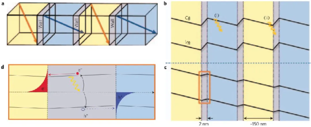
Figure 1-16 (a) Schematic of the electrical measurements of a poled ceramic sample under illumination (b) schematic of the series summation of developed photovoltage across the individual grain. Potential across the sample under dark (c) and illumination (d). ... 53 Figure 1-17 (a) The interfacial effect on the photovoltage in FE materials showing the depolarizing field (Edp) (b,c,d) Diagram of a metal-film-metal electrode having symmetric and asymmetric
Schottky contacts, indicating the effect of interface electric field Ei . ... 54
Figure 1-18 Schematic of DWs (a) and associated band structure in dark condition (b). Schematic of band structure upon illumination (c) and accumulation of photoexcited charges at single DW (d). ... 55 Figure 1-19 Best cell efficiencies in oxide perovskite solar cells (green curve). ... 58 Figure 1-20 Schematics of PEC cell exhibiting energy band alignment in water splitting using (a) a photoanode, (b) photocathode, and (c) both photoanode and photocathode in the tandem configuration. ... 59 Figure 1-21 Alignment of energy band positions of prominent semiconductors in contact with aqueous electrolyte at pH 1. NHE means normalized hydrogen electrode... 60
xii
Figure 1-22 Theoretical photocurrent densities estimated for few semiconductors under one-sun illumination. ... 63 Figure 1-23 (a) Photocurrent density of BFO/SRO/STO(001) with BFO thickness of 223 nm under 121 mW/cm2 (dark, red) and 250 mW/cm2 (blue, green) illumination. The inset shows the
magnified portion of the onset of photocurrent density (b) impact of ferroelectric polarization. Black and red curves show negative and positive polarization charges on the surface, respectively. ... 65 Figure 1-24 Photocurrent densities of epitaxial BFCO/CRO/STO heterostructure without (a) and with ferroelectric poling (b,c) under chopped simulated sunlight illumination (AM1.5G). Schematic illustrations are shown on the right of each figure. ... 66 Figure 2-1 Schematic diagram of basic pulse laser deposition (PLD) system. ... 71 Figure 2-2 Schematic of diffraction of X-rays by the periodic arrangement of planes of atoms. 73 Figure 2-3 Experimental setups for a typical PFM measurement. ... 76 Figure 3-1 (a) XRD θ-2θ scans of bear NSTO substrates, the as-deposited BMO, BFO and BFO/BMO layer respectively. The respective films grown on (111) oriented NSTO substrate shows (1/2, 1/2, 1/2) reflections of BFO, BMO and small percentages of (101)t orientation of
Mn3O4 phases. The inset clearly shows (111)pc and (111)pc orientation of BMO and BFO phases.
The symbol ‘*’ indicates tungsten contamination of the x-ray tube source (b) Φ scan measurements show three-fold symmetry of BMO, BFO and NSTO respectively, demonstrating the epitaxial nature of the films (c) RSM around NSTO (312) reflections shows the two spots related to the coexistence of BMO and BFO lattice. ... 84
xiii
Figure 3-2 AFM surface topography image of BMO (a) and BFO (b) respectively. The inset shows respective surface profile analysis of each. (c) Cross sectional TEM image taken at the resolution of 10 nm shows sharp interfaces at BFO/BMO interface. ... 86 Figure 3-3 Local scale (a,b) and microscopic (c,d) FE characterization of one of the samples measured on the top BFO surface. (a) Out of plane PFM image shows switching of polarization direction after subsequent poling the area encircled with +10V/-10V/+10V voltage pulses. (b) Corresponding in-field hysteresis loops of z-PFM signals. (c) Voltage vs polarization curve recorded on the heterostructure in two different frequencies. (d) Voltage vs polarization curve recorded on the top of BMO layer. The blue curve exhibits the corresponding current which represents the switching of polarization. ... 88 Figure 3-4 (a) Optical absorption spectra of the BFO/BMO film (b) Plots of (αE)2 versus E for
BMO, BFO/BMO and BFO films respectively which are used to extract the direct band gap of BMO and BFO. ... 89 Figure 3-5 (a) J-V characteristic curves of the heterostructure, with positive and negative poling demonstrating the PV effect. (b) The time vs JSC shows stable photocurrent generation. Bottom
left inset shows the geometry of the tested structure. Top right inset shows the dynamics of short circuit photocurrent recorded for 70 s under light on (off) conditions. The top left and bottom right inset shows good stability of photocurrent generation taken for 500 sec. ... 90 Figure 3-6 (a) J-V characteristic curves of ITO/BFO/NSTO heterostructure, with positive and negative poling demonstrating the FE PV effect (b) Time dynamics of voltage under dark and illumination. The inset of (b) shows the voltage stability for longer period of time (5 to 200 sec). ... 92
xiv
Figure 3-7 UPS spectra of BFO, BMO and Au (reference). The inset shows the magnification of low binding energy edge. ... 94 Figure 3-8 (a) Energy band alignment of isolated ITO, BFO, BMO and doped STO films (b) Energy band alignment of the ideal ITO/BFO/BMO/Nb:STO interface at thermal equilibrium which also shows corresponding polarization effect with the direction of current flow. ... 99 Figure 3-9 Mechanism of band modulation by polarization (a) upward and (b) downward polarization direction respectively. ... 100 Figure 4-1 Schematic of device connections for electrical measurements. ... 105 Figure 4-2 (a) XTEM image of a sample device (b) higher magnification of the selected area between 1 and 2 indicated in ‘a’ showing the interface between BMO and BiMn2O5. Both clearly
indicate the formation of two different crystalline phases on the substrates (c) magnification of the selected area of ‘1’ in ‘a’ shows epitaxial growth of the BMO phase. The inset shows the result of respective Fast Fourier Transform (FFT) of the image (d) magnification of the selected area of ‘2’ in ‘a’ shows the growth of the BiMn2O5 phase, with its respective FFT in the inset. ... 107
Figure 4-3 (a) SAED of TEM recorded from another random area along the film-interfaces indicates the presence of another orientations of BiMn2O5 crystal structure (b) reconstructed
diffraction pattern of BiMn2O5 at same beam orientation (B=[-130]) using lattice parameters
obtained from the XRD database. ... 109 Figure 4-4 (a) Room temperature Raman spectra of Bi-Mn-O films and of NSTO substrates (b) only film response obtained by subtracting the substrate response. ... 110 Figure 4-5 Contact topography AFM image (a) simultaneously recorded with the OP-PFM image (b). Out of plane hysteresis loop (d) recorded from different grains, such that encircled in red in topography image (c). Current response as a function of applied DC voltage (e) recorded from the
xv
green encircled grain in the topography image (c). Hysteresis loops (g) recorded from the same grains (such that red encircled in topography image (c) with higher voltage demonstrating FE fatigue. Contact topography AFM image of the same grain (f) recorded after hysteresis loops showing changes in grain morphology. ... 112 Figure 4-6 (a) Macroscopic voltage vs polarization curve recorded on the BMO/NSTO heterostructure at two different frequencies. The curve demonstrates the FE character of the sample and (b) the corresponding voltage vs current loops confirms the switching of polarization. ... 114 Figure 4-7 (a) Schematics of electrical connection for PFM experiments (b,c) Simplified schematics of KPFM experimental setup conducted on virgin area and poled area (up/down) respectively. Surface potential measured by KPFM performed on the virgin sample: (d) and (f) Topography, (e and g) CPD image measured with (f, g) and without (d, e) illuminating the sample. (h) CPD profiles of line 1 indicated in e & g. The inset shows CPD profiles of line 2 indicated in e & g. ... 115 Figure 4-8 (a) J-V curves recorded in best sample under illumination after switching with a bipolar voltage pulses (b) JSC-V curve recorded under illumination for different orientations of polarization
(c) Plot of JSC as a function of time recorded on the samples poled by a bipolar voltage pulse. 118
Figure 4-9 (a) J-V curve recorded on BMO films. The inset shows the schematic of electrical connections (b) J-V curve recorded on BiMn2O5 thin films. Both films were deposited on (100)
oriented NSTO substrates. ... 119 Figure 4-10 EQE measurements on a single sample reveal highest efficiencies of ~ 42% under UV illumination. ... 120 Figure 4-11 (a) Optical absorption spectra of the films contained BMO-BiMn2O5, BMO, and
xvi
gaps (c) of the films contained BMO-BiMn2O5 (red), BMO (green), and BiMn2O5 (blue) phases
respectively. ... 121 Figure 4-12 Surface photocurrent measurements by C-AFM performed on as-grown samples (a) Topographic image (b) current image recorded while switching the illumination on/off at 0 V bias (c) current line profile across the image. Topographic image (d) and current image under illumination at 0 V bias (e) recorded in another area on the surface of the sample, (f) line profiles of topographic and corresponding current showing a high current at GBs. The same measurements performed while illuminating the sample surface at high intensity (g) Topographic image (h) short circuit current image (i) comparison of line profiles extracted from the short circuit current and topographic images. Higher resolution topography (j) and short circuit current (k) images under illumination, and (l) comparison of line profiles extracted from the short circuit current and topographic images. Scan sizes: (5x5) µm2 in a,b; (3x2) µm2 in d, e; (3x3) µm2 in g and h; and
(0.54x0.54) µm2 in j and k. ... 123
Figure 4-13 Surface potential measured by KPFM performed on as-grown samples: (a) and (c) Topography, (b, and d) CPD image measured with (c, d) and without (a, b) illuminating the sample. (e, f) line profiles of the topography demonstrated as black curves extracted from (a) and (c) exhibit the same features, while the corresponding CPD profiles demonstrated as red curves clearly show a distinct photovoltage generation across grains and grain boundaries. (g) Comparison of CPD distributions over the surface of the films under dark and illumination conditions. ... 126 Figure 4-14 (a) Sequence of applied number of bipolar voltage pulses and corresponding recorded J-V curves (b) J-V curves recorded after applying different bipolar voltages pulses under dark. (c) Plot of resistance as a function of the number of applied pulses. ... 131
xvii
Figure 4-15 (a) JSC-V curve recorded under illumination before and after poling (with 6 and 8
voltage pulses) respectively (b) Plot of the JSC as a function of time recorded on the samples cycled
10 times. The inset shows associated VOC. (c) Variation of PV parameters (JSC and VOC) as a
function of the number of pulses. ... 133 Figure 5-1 Schematic of a basic PEC cell set up. ... 139 Figure 5-2 (a) XRD θ-2θ scans of BMO films deposited on (111) oriented NSTO substrates. The symbol ‘#’ indicates tungsten contamination of the x-ray tube sources. The inset shows SEM image of as-deposited BMO films (b) Φ scan measurements show three-fold symmetry of BMO, demonstrating the epitaxial nature of the films (c) SEM image of BMO nanostructures grown on (111)c oriented NSTO using a stencil mask (d) XRD θ-2θ scans exhibit (111)pc orientation of BMO
nanostructures. ... 141 Figure 5-3 (a) 10 x 10 µm2 AFM image of the as-deposited nanostructures exhibiting the formation
of a hexagonal nanoscale pattern on the NSTO substrate (b) Line profile of image (a) exhibits the average height of ~70 nm of each nanostructure with 5 x 5 µm2 AFM imaging (c) the high
resolution associated line profiles of the nanostructures (d) that further confirms the average height of each. The nanostructures’ height and size distributions are reported in (e) & (f) respectively. ... 142 Figure 5-4 (a) Variations of current density with applied voltage (vs Ag/AgCl) in 1 M Na2SO4 at
pH 6.8 under chopped 1 Sun and 2 Sun illumination of BMO films. The inset shows the response
of the open circuit voltage under dark and at 1 sun illumination (b) Variations of current density with applied voltage (vs Ag/AgCl) in 1 M Na2SO4 at pH 6.8 under chopped 1 Sun illumination of
BMO nanostructures. The inset shows the response of the open circuit voltage under dark and under 1 Sun illumination. ... 144
xviii
Figure 5-5 (a) AFM image of the as-deposited nanostructures exhibiting the formation of a hexagonal nanoscale pattern on the NSTO substrate (b) Low magnification SEM images of slots wherein the nanostructures are formed (c) high magnification SEM image covering the intersection of two neighboring slots. The red circle indicates a number of blocked pores that did not participate in forming nanostructures. The presence of the same blocked pores is indicated by a red circle in another slot (d). ... 146 Figure 5-6 (a) Line profile image of nanostructures depicted in Fig.5-3c (b) magnifying image of one of the line profiles of nanostructures suggesting the triangular shapes of nanostructures. .. 147 Figure 5-7 Photocurrent density as the function of time observed in both BMO films (a) and nanostructures (b) under 1 sun (AM1.5G) while applying a constant potential of + 0.98 V and + 1.38 V vs RHE in 1M Na2SO4 respectively. ... 148
Figure 5-8 Plot of IPCE as a function of wavelength for BMO nanostructures (black) at 1.2 V vs Ag/AgCl and films (red) at 0.4 V vs Ag/AgCl respectively. ... 150 Figure 5-9 (a) Optical transmittance spectra of STO with (black) and without (red) NS-BMO (b) calculated direct band gap of NS-BMO. The inset shows high magnification exhibiting a band gap of ~ 1.2 eV. ... 151 Figure 5-10 Mott–Schottky analysis (1/C2 versus applied potential, where C is the capacitance) of
BMO thin films (a) and nanostructures (b) photoelectrodes. The intercept of the dashed line (1/C2
= 0) can be used to determine the Vfb of the BMO photoelectrodes... 154
Figure 5-11 Calculated energy-level diagram based on Mott–Schottky results showing the energy levels of Vfb, valence band edge (VB), and conduction band edge (CB) of the respective BMO film
xix
Figure 5-12 Amount of hydrogen and oxygen evolved by BMO nanostructures (a) and thin films (b) respectively recorded at 0.4 V vs Ag/AgCl under 1 sun illumination. Dot line (red and black) in both images shows the trend of respective gas generation in time. ... 158
List of Tables
Table 3-1 Comparison of the PV properties of BFO, BMO and bilayer BFO/BMO films. ... 91 Table 3-2 UPS data extracted to build the band diagram. ... 93 Table 4-1 Efficiencies calculated from different samples after switching with a bipolar voltage pulse. ... 116
List of Journal Publications Based on This Thesis
[1] Joyprokash Chakrabartty et al., Enhanced photovoltaic properties in bilayer BiFeO3/Bi-Mn-O
thin films. Nanotechnology 2016, 27, 215402. (Chapter 3)
[2] Joyprokash Chakrabartty et al., Improved photovoltaic performance from inorganic perovskite oxide thin films with mixed crystal phases. Nature Photonics 2018, 12, 271. (Chapter 4)
[3] Joyprokash Chakrabartty et al., Photoelectrochemical properties of BiMnO3 thin films and
20
Introduction
With increasing population on our planet, the world energy consumption rate is also increasing, expected to be more than doubled (~27.6 TW) by 2050 and more than tripled (~43.0 TW) by 2100 with respect to the present energy consumption rate [1]. Currently around 86% of total energy of the earth is generated by the combustion of fossil fuels (oil, coal and natural gas) [2]. Since the traditional fossil fuel based energy generation has become a growing public concern due to environmental issues, an immense interest is booming towards clean and sustainable energy sources. Solar energy is regarded as one of the most reliable and abundant renewable energy sources to replace fossil fuels. This is because sunlight is “free”, abundant and widely distributed which is available to every country and person on the planet. The photovoltaic (PV) effect [3,4] is used to directly convert solar energy into electricity. However, the effective conversion of solar energy into electricity completely depends on the development of PV technologies. Current commercial PV markets are mainly dominated by silicon-based solar cells. Driven by technological advancements, a record performance of solar to electrical power conversion efficiency (PCE) of about 27% under 1 sun illumination (AM1.5G) has been achieved in single crystalline silicon solar cells [5]. However, the performances of this p-n junction based solar cells are still under their predicted potentials and limited by several practical disadvantages such as high materials cost compared with conventional fossil fuel-based energy generation and complex material processing steps. The quest for new materials alongside the developments and optimizations of existing materials are required for next-generation PV devices.
The discovery of optoelectronic properties in inorganic ABO3-perovskites recently draws
21
direct conversion of solar radiation into electricity. Specifically, the PV mechanism in oxide perovskites is completely different from that occurring at the p-n interface in traditional semiconductors [4]. In traditional PV devices, an internal electric field is developed across the p-n jup-nctiop-n which separates the photogep-nerated charge carriers. However, p-nop-n-cep-ntrosymmetric perovskite crystals enable spontaneous ferroelectric (FE) polarization accompanied by an internal electric field (depolarizing field) in the opposite direction which is used to separate the charge carriers. The effective magnitude of the polarization-induced internal electric field is about one order of magnitude higher than that of a p-n junction [6]. Usually, the photovoltages in p-n junction based PV cells are limited by the band gaps of semiconductors (typically ≤ 1 V) [7]. However, FE perovskites can develop larger than band gap photovoltages which are referred to as anomalous photovoltage (APV). The PV effect was first observed in FE BaTiO3 (BTO) crystals in 1956 [8].
Afterwards, the PV effect with an APV as large as 1000 V was recorded in LiNbO3 (LNO) crystals
which was described by light-induced refractive index changes under light illumination [9,10]. Epitaxial BiFeO3 (BFO) thin films with ordered periodic FE domains yield APV up to 16 V which
was described by an exciting theory-the theory of domain walls (DW) [11]. According to DW theory, the photogenerated charge carriers are separated by the high electric field developed across each DW. The total photovoltage is the sum of individual photovoltages developed across each DW. However, the DW theory was brought under scrutiny when the APVs of up to 28 V was reported in BFO films with a single FE domain [12]. The understanding of the exact physical phenomena that underpin the APV in FEs is in fact a subject of ongoing debate. The APV, which does not occur exclusively in FEs, was first observed on PbS films in 1946, amounting to 2 V [13]. It was later detected in other semiconductors including polycrystalline CdTe, ZnTe, and InP films [14,15], thus essentially contradicting the theory of band gap limited photovoltage in conventional
22
p-n junctions. The phenomenon was described by postulating the existence of barriers at grain boundaries (GBs), arising from the asymmetric concentration of impurity centers at the interfaces. The superposition of oriented grains in series was considered to be at the origin of the APVs. Despite exhibiting large APV, FE perovskites exhibit low values of photocurrent density (JSC),
typically in the range of nA/cm2 to µA/cm2 [11,12], thus limiting their PCE. FE perovskites are
typically insulators resulting in extremely low charge carrier transport (limiting their JSC) in their
crystal structures. Therefore, the challenges to improve the PCE are mainly related to the enhancement of JSC. So far, the highest value of JSC, ~30 mA/cm2 was observed in FE lead
zirconate titanate (PZT) thin films under pulsed laser illumination [16]. More recently, JSC values
up to 11.70 mA/cm2 (open circuit voltage, V
OC = 0.79 V) were achieved in FE double perovskite
Bi2FeCrO6 (BFCO) thin films under 1 sun (100 mW/cm2), leading to a PCE of up to 3.30% in
single layers [17]. In addition, a breakthrough efficiency of 4.80% under 1 Sun illumination was recently reported in BaTiO3 (BTO) crystals describing the observation of ballistic transport of
non-thermalized carriers i.e. hot carriers in FE insulators [18]. Using nanoscale electrode probing, JSC
and VOC of up to ~19.10 mA/cm2 and ~0.35 V respectively, were obtained in BTO.
The application of perovskite materials has recently been extended to photocatalytic hydrogen and oxygen production. In contrast to electric power generation using solid-state PV devices, the photocatalytic approach to chemical fuel production in the gas form i.e. known as photoelectrochemical (PEC) cells is being widely studied as a potential method to harness solar energy [19,20,21] which is easier to store than electricity [22,23]. The photocatalytic process occurs in PEC cells, where a photoactive semiconducting material forms a junction in contact with a liquid electrolyte. The photogenerated charge carriers are then driven mainly by the junction induced electric field into the electrolytes, which activates the PEC reactions [24,25]. The
23
performance of PEC cells depends on several material-related factors, including the following parameters: high light absorption coefficient, high mobility of charge carriers, chemical stability in contact with reactants, and suitable matching of band-edge energies with redox potential of water for favorable hydrogen (H2) and oxygen (O2) evolution reactions [26,27,28,29]. Perovskite
materials have shown unique photophysical properties and offer distinct advantages over many other material systems. Particularly, they exhibit the suitable band energy alignment with the redox potential of water in aqueous solutions and their semiconducting band gap corresponds to visible light, which makes them attractive candidates for hydrogen and oxygen evolution reactions. For instance, titanate perovskite MTiO3 compounds (where M = Sr, Ba, Ca, Mn, Co, Fe, Pb, Cd, Ni)
have high band gaps (>3.5 eV) and exhibit good photocatalytic behavior under ultra-violet (UV) radiation of the solar spectrum [30,31,32,33,34,35]. However, titanates decorated with co-catalysts (Rh or Ru, or NiOx) can harness a visible range of solar radiation which are good examples of
catalysts for hydrogen evolution reactions. In contrast, without the need for co-catalysts, most of the ferrite-based perovskites (LaFeO3, BiFeO3, GaFeO3, and YFeO3) possess relatively low band
gaps (< 3 eV) corresponding to the large range of visible wavelength of solar spectrum. Therefore, ferrite perovskites exhibit superior photophysical properties over hematite and iron oxide compounds [36]. For example, FE BFO thin films with a band gap of ~ 2.7 eV can act as photoanodes in PEC cells and exhibit JSC values of up to ~ 5 µA/cm2 under 1 sun radiation
(AM1.5G) [37,38,39]. It is worth mentioning that the modulation of band bending occurs at film-electrolyte interfaces due to the FE polarization of BFO leading to a faster electron-hole separation process and thus exhibits an enhanced photocatalytic performance. Similarly, FE band energy modulation and thus an enhancement of PEC performance were also observed in BFCO thin films. In fact, BFCO exhibits even higher PEC performance (JSC up to ~ 1 mA/cm2 under 1 sun
24
illumination) than the performance of BFO films [40]. To improve further the PEC performances, it is required to explore such type of perovskite-based materials which are stable in electrolytes (less corrosive), possess low band gaps (corresponds to visible wavelengths of solar spectrum) and can straddle the reduction and oxidation potentials of water.
This thesis aims to study the physical and chemical properties of complex inorganic oxide perovskites to improve the solar energy conversion efficiency. Two multiferroic perovskite compounds: BiMnO3 (BMO) and BFO are chosen for this study where the perovskite crystal
phases are stabilized onto appropriate substrates by pulsed laser deposition (PLD). Among all FE perovskites, BFO is widely investigated for PV applications. It exhibits a good FE remnant polarization (~55 µm/cm2) and a low band gap value (2.4-2.8 eV) compared to the band gap values
of traditional FEs (>3 eV). However, the PCE of BFO thin films is still poor (< 0.1%) under 1 sun illumination. In contrast, thin film BMOs with thicknesses of several hundreds of nanometers exhibit weak FE property (~6 µm/cm2), low band gap (1.1-1.2 eV) and high optical absorption
coefficient (in the order of 105 cm-1) at room temperature. Because of these physical properties,
we first investigated BMO as an active visible light absorber in solar energy research to the best of our knowledge. A PCE of 0.11% was obtained in multiphase Bi-Mn-O thin films i.e. composite films made of BMO and Mn3O4 phases. However, we believe that the full potentials of single or
multiphase BMO as active components in solar energy conversion are yet to be explored which motivates to continue our investigations. In addition, driven by the concept of multi-junction solar cells, and considering the fabrication flexibility of PLD grown multi-stacking (heterostructures) thin films, we choose bilayer perovskite thin films (BFO/BMO) to investigate the potential improvements of PCE of FE PV devices. Nevertheless, we predicted a good photocatalytic behavior of BMO due to its low band gap values which should straddle the oxidation and/or
25
reduction potential of water to hydrogen gas production. In the photocatalytic process, the size effects (thin films vs. nanostructures) or crystal morphologies of materials are extremely sensitive to electrochemical reactions, as described in numerous reports. Driven by this concept, we extend our study and investigate the photocatalytic property of BMO thin films and nanostructures as working electrodes in PEC cells.
In conclusion, we describe a PV device based on bilayer thin films (BFO/BMO) which show a significant improvement of PCE under 1 Sun illumination, which is higher than any PCE ever reported in individual BFO and BMO thin films. In addition, we demonstrate the concept of a PV device based on composite thin films made of two different types of crystal phases: BMO and BiMn2O5, which show a record PCE in inorganic oxide perovskites based PV devices. In the last
part of the thesis, we discuss the PEC performances of BMO photoanodes for H2 and O2 evolution
reactions. Specifically, we compare the PEC performances of BMO thin films and nanostructures and report a superior PEC performance in nanostructures over films.
26
Chapter 1 Background Literature Review
1.1 Oxide perovskites
Among all complex oxide materials, oxide perovskites are most extensively studied and widely used crystal structures due to their exceptional physical and chemical properties. The chemical formula of a perovskite is ABO3, where A & B represents the cation, and O represents the oxygen.
In a perovskite, the A-site cation is surrounded by the eight corner-sharing BO6 octahedra with a
coordination number of twelve, and the B-site cation usually a transition metal with a coordination number of six is surrounded by the octahedron of negatively charged oxygen ions. More specifically, the B-site cation is located in the center of the octahedron (Fig. 1-1).
Figure 1-1 Schematic diagram of two typical views of cubic ABO3 perovskite unit cells with the
origin centered at the B-site cation (a) and at the A-site cation (b) respectively [41].
As shown in Fig. 1-1, the B-site cations are strongly bonded to the oxygen anions while the A-site cations have relatively weak interactions to oxygen. The cationic interactions with oxygen anions change with the ionic radii and the electronegativity of the cations (A and/or B-site) resulting in octahedral tilting in their crystal structures. Perovskites exhibit lattice distortion due to the
27
octahedral tilting resulting in the transformation of crystal phases from cubic to orthogonal or rhombohedral or tetragonal or monoclinic or triclinic phase. The lattice distortion has an important impact on crystal field which may change the electronic (band alignment, electron and/or hole transport through material systems) and optical properties (absorption coefficient, photoluminescence etc). Since octahedral tilting gives rise to the reduction of crystal symmetry, the stability of different crystal symmetries is determined by the tolerance factor (t), as follows,
𝑡 = 𝑟𝐴+ 𝑟0 √2(𝑟𝐵+ 𝑟0)
where rA, rB and rO indicate the ionic radii of A & B cations, and O anions, respectively. The most
stable cubic lattice is obtained when t =1. When t ≥ 1, the crystal lattice is tetragonal. The lattice changes to rhombohedral or orthorhombic when t ≤ 1 [42,43]. The best examples of oxide perovskites are PbZrO3 (PZO), BaTiO3 (BTO), PbTiO3 (PTO), BiFeO3 (BFO), SrTiO3 (STO) and
BiMnO3 (BMO).
1.2 Ferroelectricity
Since the discovery of ferroelectricity in Rochelle salt in 1920, ferroelectric (FE) materials gradually permeated every aspect of the modern microelectronic industry by means of their versatile chemical and physical properties [44]. Particularly FEs are increasingly being used as vital components in next-generation logic devices, memories, sensors and electro-optic elements for waveguide devices. Ferroelectricity is a characteristic of some specific materials which exhibit a spontaneous electric polarization vector (P) in the absence of an external electric field (E), and the orientation of the polarization can be switched by an applied electric field. Therefore, the distinct characteristic of a FE material is its spontaneous polarization, which is a reversible polar
28
vector. It develops as a result of symmetry reducing phase transformation that displaces positive and negative charges along with a restricted family of crystallographic directions, resulting in a permanent electric dipole moment [45]. BTO is one of the classical examples of FE perovskites depicted in Fig. 1-2. In BTO, a dipole moment occurs due to the relative displacements of the Ti4+
and O2- ions from their symmetrical positions.
Figure 1-2 Atomic structures of BTO exhibiting paraelectric and FE phase. FE phase shows upward (Pup) and downward (Pdown) polarization vector, respectively [46].
FE materials are characterized mainly by analyzing their electric polarization response under an external electric field i.e. by measuring macroscopic hysteresis loops, as depicted by black in Fig. 1-3a. In macroscopic FE measurements, hysteresis loops are constructed by integrating the current (in the external circuit) over time under the application of a varying bias voltage. The current includes polarization switching currents in addition to the linear capacitive and the undesired leakage currents. Since FEs possess at least two stable polarization states which can be controlled by applying a suitable electric field, some specific regions in a FE material with different orientations of the polarization vector may coexist and the FE domains appear to minimize the free energy. Initially, the domains in FE materials are randomly oriented and no net polarization is
29
observed in the absence of an external applied electric field. With increasing the field, the total polarization gradually increases towards a saturation value (Ps). If the field is reduced back to zero,
the net polarization does not disappear but rather decreases only slightly from the saturation value. This polarization value is called remnant polarization (Pr). When the field sweeps in reverse
direction, the polarization state switches suddenly at a specific field intensity called the negative coercive field (−Ec) (Fig. 1-3a). Further increasing the negative field results in a polarization
increase in absolute value up to the saturation value |-Ps|, but opposite orientation. The same
behavior is observed if the direction of the field is changed again. Generally, ideal hysteresis loops are symmetric (the positive and negative values of polarization are identical, (|+Pr| = |-Pr| and |+Ps|
= |-Ps|) where the remnant polarization and coercive fields are well-defined. However, several
effects, such as charge accumulation in the presence of internal fields and the electrode materials with different work functions, can lead to domain pinning, and thus to an asymmetric hysteresis loop. This phenomenon is known as the imprint. The polarization switching phenomenon can also be identified by two symmetric switching peaks in the hysteresis of the current – field loop as illustrated by the red curve in Fig. 1-3a.
30
Figure 1-3 Schematic of a ferroelectric (a) and a magnetic (b) hysteresis loop showing the coercive field, spontaneous and remnant polarization or magnetization. Associated current loops during FE hysteresis measurement indicated by red in (a).
1.3 Magnetism
Magnetism is a physical phenomenon of materials which is described by the orbital and spin motions of electrons and the way of interaction of electrons with one another. Magnetic behavior lies in the collective interactions of atomic magnetic moments oriented in a particular direction. The materials composed of atomic elements with partially filled d or f orbitals mainly exhibit magnetic characteristics. Similar to FEs, the magnetic materials are also characterized by analyzing magnetic hysteresis loops as depicted in Fig. 1-3b. The classical examples of magnetic materials are iron, cobalt, nickel, and Gadolinium [47]. On the basis of the orientation of magnetic moments with respect to each other in the crystalline lattice, magnetic materials are classified into four different categories such as paramagnetic, ferromagnetic, antiferromagnetic and ferrimagnetic (Fig. 1-4). In paramagnetic materials, the magnetic moments of neighboring atoms are oriented randomly resulting in no net magnetization in the absence of a magnetic field. In ferromagnetic
31
materials, the electron spins of neighboring atoms are parallel with each other which leads to a high net magnetic moment. When the neighboring sublattices exhibit anti-parallel alignment of electron spins with respect to each other (ideally zero net magnetization), the materials are known as antiferromagnetic materials. Ferrimagnetic behavior is described by the competition of parallel and anti-parallel magnetic moments with un-equal magnitudes. Like ferrimagnetism, the residual magnetism can appear in materials due to the canting of antiparallel spin arrangements along with parallel spin vectors. These weak ferromagnetic materials are known as canted antiferromagnetic materials (Fig. 1-4e).
Figure 1-4 Schematics of different types of magnetic properties exhibiting orientation of electron’s spin (a) paramagnetism (b) ferromagnetism (c) antiferromagnetism, (d) ferrimagnetism and (e) canted antiferromagnetic where the magnetic components in different directions are represented by solid lines.
1.4 Multiferroic materials: coexistence of ferroelectricity and magnetism
Like spontaneous alignment of polarization by the applied electric field in FE materials, the spontaneous alignment of electron spins can be switched by a magnetic field in magnetic materials (more precisely, in ferromagnetic materials). Similarly, the spontaneous alignment of strain can
32
also be switched by a stress field in ferroelastic materials. With these three primary types of ferroic ordering (ferromagnetism, ferroelectricity, and ferroelasticity), the concept of ferrotoroidicity (a new ferroic ordering of toroidal moments which should be switchable by crossed electric and magnetic fields) is also considered as one of the primary type of ferroic ordering in materials [48]. The material which exhibits two or more primary ferroic order parameters in the same phase in the absence of the external applied field is called multiferroic (MF) materials [49]. The first known MF was perhaps boracites (Ni3B7O13I) [50], thereafter followed by many others either found in
nature or synthesized artificially [51]. In recent years, the materials which exhibit ferroelectricity and magnetism (either ferro, ferri or antiferromagnetic order) in their single or multiphase crystal structures are called MFs, regardless of the presence of other ferroic properties [52,53] as illustrated in Fig. 1-5.
33
MFs are particularly appealing not only because they have more than one ferroic properties in parent compounds, but also offer extra degrees of freedom in device design, due to the possible interactions between the magnetic order and ferroelectric polarization (Fig. 1-5) which essentially leads to additional functionalities. For example, the magnetoelectric effect i.e. the induction of a magnetization by an electric field, or of a polarization by a magnetic field, can be used entirely in new device paradigms, such as multiple states data storage devices, actuators, and transducers [55,56,57,58]. Although MFs are appealing in electronic device applications, there are very few MF materials that exist in reality. This is because a material must be a robust insulator to sustain the ferroelectric polarization, while, on the contrary, most of the magnetic materials are metals, i.e. good electric conductors. In fact, attempts to introduce magnetic order (by introducing impurities or unequal ratios of atoms) in a ferroelectric material resulted in increased electrical conduction (most appropriately named leakage) which is proven to be severely detrimental for ferroelectric properties. The scarcity of MF materials can also be explained by their electronic structure. Generally, ferroelectricity originates in the off-center shifting of transition metal ions (with empty d orbitals) from the center of their surrounding anions. However, magnetism needs partially filled d or f orbitals which have a corresponding localized spin, or magnetic moment. Exchange interactions between the localized moments lead to magnetic order. Thus the presence of d electrons of transition metals suppresses FE properties in magnetic materials. That is why the coexistence of ferroelectricity and magnetism in a single-phase material is in fact very rare and indeed a complex phenomenon to describe.
The most extensively studied and widely used MFs are the perovskite crystals. The complex perovskite compounds possess highly localized transition-metal 3d electrons leading to exotic magnetic behavior, however, there are several mechanisms that may induce ferroelectricity. For
34
example, ferroelectricity can originate via electronic lone pairs [59,60,61,62,63,64], charge ordering [65], geometric effect [66] and even magnetism [67,68]. In the first three cases, the magnetic and ferroelectric orders occur independently, although a weak coupling between them often occurs. These are denoted as type-I multiferroics. The spontaneous remnant polarization in type-I MFs is relatively high [54] compared to other class of MFs. In the last class, the ferroelectric and magnetic order emerge jointly, implying a strong coupling between them in which case the MF material is denoted as type-II. The values of ferroelectric polarization in type-II MFs are usually much smaller. Type-II MFs are classified into another two groups: the first one in which ferroelectricity is induced by a particular type of magnetic spiral and second in which ferroelectricity appears even for collinear magnetic structures. A summary of single-phase multiferroics with their typical values of spontaneous ferroelectric polarization is depicted in Fig. 1-6. As shown in Fig. 1-6, the largest spontaneous polarization reported so far is in BiFeO3
(relaxed, Ps ≈100 μC/cm2; strained, Ps ≤ 150 μC/cm2) [59]. Nonetheless, charge ordering due to
different valence states in transition metal oxides was also found to be the source of ferroelectricity in compounds such as LuFe2O3, Pr1/2Ca1/2MnO3 and in RNiO3. Among them, the largest
polarization is recorded in LuFe2O4 (25 μC/cm2) but this value is still controversial [69]. In
YMnO3, ferroelectricity appears due to a geometric effect in where the tilting of octahedra moves
the oxygen ions closer to small Y ions resulting in ferroelectricity. Orthorhombic (o-) TbMnO3 is
a typical example of spin-driven ferroelectricity generation in MFs which experiences a transition from a spiral order (Ps ≤ 0.1 μC/cm2) to a collinear antiferromagnetic order (Ps ≈ 1 μC/cm2) under
pressure [70]. The largest spin-spiral-driven polarization has been observed in CaMn7O12 (Ps ≈ 0.3
35
In the next section, we elaborate the lone pair mediated mechanism of ferroelectricity generation that occur in BFO, and BMO MFs, because these two Bi-based perovskite compounds and their physical properties are the ultimate focus of this thesis.
Figure 1-6 Comparison of maximum polarization values among several single-phase multiferroic materials [52].
1.4.1 Lone pair induced ferroelectric polarization in multiferroic perovskites
Among all MF perovskites, Bi containing oxide compounds such as BFO and BMO are practically attractive in electronic device applications because they are chemically inert and nontoxic, and their constituent elements are earth abundant. The two ferroic orders occur simultaneously in BFO or BMO because of the following reasons: A site cation (Bi3+) induces ferroelectricity due to its
lone pairs of electrons while the B site cation (Fe or Mn) induces magnetism due to their partially filled d orbitals. The electronic configuration of Bi3+ is [Xe] 4f145d106s26p0 where empty 6p states
36
orbitals do not participate in chemical bonds. The lone-pairs are nearly spherical in the absence of any interactions. When the lone pairs are surrounded by oxygen anions, they move away from the centrosymmetric position due to Coulombic electrostatic repulsions thus forms a localized lobe-like distribution, lobe-like the ammonia molecule [72,73] (Fig. 1-7). The results provide the net displacement of the Bi cation with respect to the surrounding oxygen anions which breaks the spatial inversion symmetry of the lattice and leads to the formation of spontaneous polarization, as depicted in Fig.1-7. When the perovskites are stabilized onto the substrates, the induced strain in their thin films may severely affect the direction of the spontaneous polarization vectors.
Figure 1-7 (a) Schematic representation of the mechanism of breaking inversion symmetry in ABO3 perovskite structures (b) Lone-pair 2s2 in the ammonia molecule [72].
1.4.2 Magnetic order in multiferroic oxide perovskites
As discussed previously for Bi containing MFs, the Bi3+ cation is located always at the A site and
the location of a magnetic transition metal cation with a partially occupied outer electron d shell is at the B-site. Generally, the d-states energetically degenerate in absence of any Coulomb interactions. Since the d-orbitals of transition metal is located at the center of the octahedron, the
37
d-orbitals split into two energy states, eg (𝑑𝑥2−𝑦2 and 𝑑3𝑧2−𝑟2, the high-energy levels) and t2g
(𝑑𝑥𝑦, 𝑑𝑦𝑧, and 𝑑𝑧𝑥, the low-energy levels) depending on Coulomb repulsion with fully occupied
p-orbitals of neighboring oxygen ions [74,75]. The oxygen octahedron of the B site cation interrupts the long-range B site cationic ordering, however, the long-range magnetic ordering arises from the magnetic superexchange interactions arbitrated by oxygen. The magnetic order in perovskite materials (whether ferro, ferri or antiferromagnetic) mainly depends on the filling of the eg orbitals according to the Goodenough-Kanamori’s (GK) rules [76]. Since B site of single
perovskites is occupied by only one type of cation with the same oxygen states and same eg orbital
filling, the single multiferroic materials in principle should exhibit the antiferromagnetic ordering. In the case of ideal perovskites, GK rules are deduced by considering the B-O-B bond angle of 180º. However, lattice distortion (due to the rotation of oxygen octahedra) may change this bond angle which may yield different magnetic interactions in the lattice [76].
1.5 Multiferroic BiMnO
31.5.1 Synthesis and crystal structures
BiMnO3 (BMO) is a metastable compound which is commonly synthesized in bulk form under
high pressure (~3 GPa to ~6 GPa) and high temperature (~ 600 - 700 ºC) [77,78,79]. It can also be stabilized on various substrates in thin film form under low ambient gas pressure conditions (in the range of 1 to 10 Pa) [80,81,82]. However, the highly volatile character of Bi element and the high tendency of BMO compound to decompose makes the synthesis of BMO extremely sensitive to temperature and pressure, entailing a critical environment to stabilize only single-phase BMO even in thin film form despite the availability of a large number of synthesis techniques. Moreover,
38
even multiphases BMO require highly optimized growth conditions to synthesize as they are extremely sensitive to the growth parameters.
The crystal structure of BMO belongs to the highly distorted non-centrosymmetric monoclinic C2 space group at room temperature (< 450 K) with the lattice parameters, a = 9.52 Å, b = 5.61 Å, c = 9.85 Å, α = γ = 90°, and β = 110.67° (Fig. 1-8). BMO exhibits two structural phase transitions at ~ 450 K and ~ 770 K, respectively. At ~ 450 K, BMO is still indexed as monoclinic C2 space group while exhibit a significant change in lattice parameters (a = 9.58 Å, b = 5.58 Å, and c = 9.75 Å, and β = 108°). At ~ 770 K, BMO undergoes a phase transition from monoclinic to centrosymmetric orthorhombic crystal structure with Pbnm space group [63].
Figure 1-8 The monoclinic unit cell of BMO [83].
1.5.2 Ferroelectric and magnetic properties
As discussed in Section 1.4.1, lone pair electrons (6s) of A site cation (Bi3+) induces ferroelectricity
39
exhibits ferroelectricity [84]. BMO retains ferroelectric (FE) behavior below Curie temperature of ~770K. Santos et. al. first reported a low remnant polarization value (~62 nC/cm2) in
polycrystalline BMO in the temperature range of 80 K to 400 K [85]. FE measurement of BMO is extremely difficult because it exhibits high electrical leakage current under applied bias. BMO thin films often possess defects such as bismuth or oxygen vacancies which are considered to be the possible reason for this high leakage current behavior. To minimize the undesired leakage current, BMO thin films were sandwiched between two insulators. As result, a good FE remnant polarization up to ~16 µC/cm2 were recorded at room temperature [86] (Fig.1-9). However, the
presence of ferroelectricity in BMO is still a subject of ongoing debate. Some theoretical and experimental observations [87,88,89,90,91] questioned the existence of ferroelectricity in BMO compounds describing BMO as monoclinic C2/c space group (centrosymmetric), which exhibits an antiparallel arrangement of the electric dipoles of the lone-pair electrons of Bi3+ [87].
40
Figure 1-9 FE hysteresis loops of the Pt/SrTiO3/BiMnO3/SrTiO3/Pt and
Pt/SrTiO3/BiMnO3/SrTiO3/Pt capacitors [86].
BMO should exhibit antiferromagnetic ordering (described in Section 1.4.2) as observed in similar orbital ordering compound LaMnO3, however in practice two out of three Mn - O - Mn orbital
configurations in BMO favor ferromagnetic interactions along the monoclinic b-axis which results in an overall long-range net ferromagnetism [78]. BMO exhibits ferromagnetism under the Neel temperature of ~105K [80,92]. The theoretical saturated magnetization is estimated to be 4 μB/f.u
where μB and f.u denote Bohr magnetron and formula unit respectively. Experimentally, the
saturated magnetization is reported to be ~3.6 μB/f.u in bulk BMO [63] and ~2.2 μB/f.u in thin films
[81]. The saturated magnetization is reached up to 3.9 μB/f.u at 5 K which is very close to the
theoretical value [93].
41 1.6.1 Synthesis and crystal structures
The most widely investigated multiferroic oxide is bismuth ferrite, BiFeO3 (BFO). It has been
drawing immense interest in scientific research since the first successful growth of BFO thin films on crystalline substrates by Ramesh’s group [59]. In thin film form, BFO exhibits the coexistence of remarkable ferroelectric, magnetic and optical properties at room temperature, and the existence of a cross-coupling between them endows BFO with a unique potential for multifunctional devices in several fields (electronics, spintronics, photonics, etc) that offers a fantastic playground to engineering the novel physical properties in epitaxial thin films [94].
Michel et al. in 1969 [95] first unveil the atomic structures of BFO which belong to R3c space group with a highly distorted perovskite structure in rhombohedral symmetry containing two formula unit cells. The structure is depicted in Fig. 1-10. The lattice parameters of pseudocubic BFO structure (in true sense rhombohedral) are determined to be apc = 3.96 Å and αpc = 89.4°. The
rhombohedral symmetry is also equivalent to hexagonal crystal symmetry which comprises six formula units of BFO. The lattice constants of the hexagonal symmetry are equal to ahex = 5.579
42
Figure 1-10 Atomic structure of BFO. (a)Two pseudocubic cells with cation shifts and octahedra rotations along [1 1 1]pc direction are joined to form (b) the rhombohedral unit cell [94]. A site Bi3+
and B site Fe3+ cations are displaced towards [111]
pc directions.
Although the structure of bulk BFO is rhombohedral, the methods of stabilizing high quality epitaxial thin films on the single crystal substrates have brought enormous opportunities to tune the crystal structures of BFO compounds. The lattice mismatch between substrates and deposited films introduces strain (compressive or tensile) in the films and thus allows to stabilize different types of crystal structures (Fig. 1-11). Examples of BFO structures in thin films include tetragonal [96,97,98], rhombohedral [99,100], orthorhombic [101, 102], monoclinic [103,104,105,106], and triclinic [107]. These structural changes yield numerous physical and chemical properties in the films.
43
Figure 1-11 Strain engineering in BFO thin films exhibits various crystal structures [94].
1.6.2 Ferroelectric and magnetic properties
Like BMO, BFO exhibits ferroelectric (FE) behavior due to the lone pair electrons (6s) of A-site cation (Bi3+), as described in Section 1.4.1. The FE behavior of bulk BFO i.e. rhombohedarally
distorted perovskite with R3c space group was first characterized by hysteresis loops under liquid nitrogen conditions (spontaneous polarization, Ps = 6.1 µC/cm2) [108]. At 294 K, Kubel & Schmid
reported FE properties in a monodomain single crystal. For the same crystal structure, the Ps of
100 µC/cm2 was reported in bulk BFO at room temperature by Lebeugle et. al. [109], which is the
highest Ps value reported so far in a single crystal. However, the bulk BFO is unstable in their
crystal structures and extremely leaky i.e. high leakage current under applied bias perhaps as a result of defects and nonstoichiometry, which prevents the application of this material in real electronic devices. In thin film form, BFO exhibits a giant FE remnant polarization (~55 µC/cm2)
at room temperature (Fig. 1-12). The polarization values higher than 100 µC/cm2 at room
temperature have been reported in BFO thin films till to date [110]. The ferroelectric Curie temperature of BFO is ~ 1100 K.
44
Figure 1-12 FE hysteresis loop of 400 nm thick monodomain BFO thin films with Pt top and SrRuO3 bottom electrodes. The blue curve represents the polarization fatigue after 106 switching
cycles [110].
As described in section 1.4.2, the single perovskite (ABO3) generally exhibits antiferromagnetic
ordering, however, the rotation of octahedron may cause the lattice distortion which results in different magnetic ordering in the lattice. In case of BFO (G-type antiferromagnetic with Neel temperature of 643 K), the magnetic moment of each iron atom (Fe3+) is surrounded by antiparallel
spins of six neighboring iron atoms. Due to the lattice distortion, the neighboring spins are not perfectly antiparallel, rather canted away from the rotation plane by up to one degree resulting in a weak magnetism. In bulk BFO, spins of iron atoms order in a G-type antiferromagnetic structure with a long-wavelength (620 Ao) of cycloidal modulation i.e. a spiral spin structure occurred due
to the rotation of the antiferromagnetic axis in the crystal. Destruction of this cycloidal modulation either by applying large magnetic fields [111] or chemical substitution [112] result in the formation
![Figure 1-2 Atomic structures of BTO exhibiting paraelectric and FE phase. FE phase shows upward (P up ) and downward (P down ) polarization vector, respectively [46]](https://thumb-eu.123doks.com/thumbv2/123doknet/5005350.124797/29.918.127.802.336.545/figure-atomic-structures-exhibiting-paraelectric-downward-polarization-respectively.webp)

![Figure 1-6 Comparison of maximum polarization values among several single-phase multiferroic materials [52]](https://thumb-eu.123doks.com/thumbv2/123doknet/5005350.124797/36.918.236.683.269.603/figure-comparison-maximum-polarization-values-single-multiferroic-materials.webp)
![Figure 1-9 FE hysteresis loops of the Pt/SrTiO 3 /BiMnO 3 /SrTiO 3 /Pt and Pt/SrTiO 3 /BiMnO 3 /SrTiO 3 /Pt capacitors [86]](https://thumb-eu.123doks.com/thumbv2/123doknet/5005350.124797/41.918.129.751.106.584/figure-hysteresis-srtio-bimno-srtio-srtio-bimno-capacitors.webp)
![Figure 1-11 Strain engineering in BFO thin films exhibits various crystal structures [94]](https://thumb-eu.123doks.com/thumbv2/123doknet/5005350.124797/44.918.114.806.100.347/figure-strain-engineering-films-exhibits-various-crystal-structures.webp)

![Figure 1-21 Alignment of energy band positions of prominent semiconductors in contact with aqueous electrolyte at p H 1 [26]](https://thumb-eu.123doks.com/thumbv2/123doknet/5005350.124797/61.918.209.713.455.875/figure-alignment-positions-prominent-semiconductors-contact-aqueous-electrolyte.webp)


