N°d’ordre NNT : 2020LYSEI055
THESE de DOCTORAT DE L’UNIVERSITE DE LYON
opérée au sein deL’institut national des sciences appliquées de Lyon
En cotutelle internationale avec
L’Université de Sherbrooke Ecole Doctorale N° 160
Electronique, Electrotechnique et Automatique
Electronique, Micro et Nano-électronique, Optique et Laser / Nanophotonique
Soutenue publiquement le 21/07/2020, par :
Michele Calvo
Étude et réalisation de capteurs
biologiques à base d'effets
plasmoniques et fabriqués sur silicium
Study and manufacturing of biosensors based on
plasmonic effects and built on silicon
Devant le jury composé de :
MONAT Christelle Professeure Ecole Centrale de Lyon Examinatrice (jury français) WEEBER Jean Claude Professeur ICB Dijon Rapporteur
LERONDEL Gilles Professeur UTT Troyes Rapporteur
MENEZO Sylvie Docteure SCINTIL Photonics Examinatrice (jury français) MELLONI Andrea Professeur Politecnico di Milano Examinateur (jury français) CANVA Michael Directeur de Recherche CNRS Examinateur
OROBTCHOUK Régis Maître de conférences INSA Lyon Directeur de thèse CHARETTE Paul Professeur Université de Sherbrooke Directeur de thèse
Département FEDORA – INSA Lyon - Ecoles Doctorales Quinquennal 2016-2020
SIGLE ECOLE DOCTORALE NOM ET COORDONNEES DU RESPONSABLE
CHIMIE CHIMIE DE LYON
http://www.edchimie-lyon.fr
Sec. : Renée EL MELHEM Bât. Blaise PASCAL, 3e étage
secretariat@edchimie-lyon.fr
INSA : R. GOURDON
M. Stéphane DANIELE
Institut de recherches sur la catalyse et l’environnement de Lyon IRCELYON-UMR 5256
Équipe CDFA
2 Avenue Albert EINSTEIN 69 626 Villeurbanne CEDEX directeur@edchimie-lyon.fr E.E.A. ÉLECTRONIQUE, ÉLECTROTECHNIQUE, AUTOMATIQUE http://edeea.ec-lyon.fr Sec. : M.C. HAVGOUDOUKIAN ecole-doctorale.eea@ec-lyon.fr M. Gérard SCORLETTI École Centrale de Lyon
36 Avenue Guy DE COLLONGUE 69 134 Écully Tél : 04.72.18.60.97 Fax 04.78.43.37.17 gerard.scorletti@ec-lyon.fr E2M2 ÉVOLUTION, ÉCOSYSTÈME, MICROBIOLOGIE, MODÉLISATION http://e2m2.universite-lyon.fr
Sec. : Sylvie ROBERJOT Bât. Atrium, UCB Lyon 1 Tél : 04.72.44.83.62 INSA : H. CHARLES
secretariat.e2m2@univ-lyon1.fr
M. Philippe NORMAND
UMR 5557 Lab. d’Ecologie Microbienne Université Claude Bernard Lyon 1 Bâtiment Mendel 43, boulevard du 11 Novembre 1918 69 622 Villeurbanne CEDEX philippe.normand@univ-lyon1.fr EDISS INTERDISCIPLINAIRE SCIENCES-SANTÉ http://www.ediss-lyon.fr
Sec. : Sylvie ROBERJOT Bât. Atrium, UCB Lyon 1 Tél : 04.72.44.83.62 INSA : M. LAGARDE
secretariat.ediss@univ-lyon1.fr
Mme Emmanuelle CANET-SOULAS INSERM U1060, CarMeN lab, Univ. Lyon 1 Bâtiment IMBL
11 Avenue Jean CAPELLE INSA de Lyon 69 621 Villeurbanne
Tél : 04.72.68.49.09 Fax : 04.72.68.49.16 emmanuelle.canet@univ-lyon1.fr
INFOMATHS INFORMATIQUE ET MATHÉMATIQUES
http://edinfomaths.universite-lyon.fr
Sec. : Renée EL MELHEM Bât. Blaise PASCAL, 3e étage Tél : 04.72.43.80.46 infomaths@univ-lyon1.fr M. Luca ZAMBONI Bât. Braconnier 43 Boulevard du 11 novembre 1918 69 622 Villeurbanne CEDEX Tél : 04.26.23.45.52 zamboni@maths.univ-lyon1.fr
Matériaux MATÉRIAUX DE LYON
http://ed34.universite-lyon.fr
Sec. : Stéphanie CAUVIN Tél : 04.72.43.71.70 Bât. Direction ed.materiaux@insa-lyon.fr M. Jean-Yves BUFFIÈRE INSA de Lyon MATEIS - Bât. Saint-Exupéry 7 Avenue Jean CAPELLE 69 621 Villeurbanne CEDEX
Tél : 04.72.43.71.70 Fax : 04.72.43.85.28 jean-yves.buffiere@insa-lyon.fr
MEGA MÉCANIQUE, ÉNERGÉTIQUE,
GÉNIE CIVIL, ACOUSTIQUE
http://edmega.universite-lyon.fr
Sec. : Stéphanie CAUVIN Tél : 04.72.43.71.70 Bât. Direction mega@insa-lyon.fr M. Jocelyn BONJOUR INSA de Lyon Laboratoire CETHIL Bâtiment Sadi-Carnot 9, rue de la Physique
69 621 Villeurbanne CEDEX jocelyn.bonjour@insa-lyon.fr
ScSo
ScSo*
http://ed483.univ-lyon2.fr
Sec. : Véronique GUICHARD INSA : J.Y. TOUSSAINT Tél : 04.78.69.72.76
veronique.cervantes@univ-lyon2.fr
M. Christian MONTES Université Lyon 2 86 Rue Pasteur
69 365 Lyon CEDEX 07 christian.montes@univ-lyon2.fr
RESUME
Les dispositifs laboratoire sur puce (ou Lab-on-a-chip ou LOC) visent à miniaturiser les procédés de laboratoires pour la détection des maladies et la surveillance des patients malades, sans avoir besoin de laboratoires médicaux. Deux exemples bien connus de LOC sont les kits de test de grossesse ou les capteurs portables du VIH.
Pour être efficaces, les appareils LOC doivent être sensibles, spécifiques à l’analyte concerné, compacts et abordables. Ces critères sont possibles grâce à un transducteur, qui peut convertir la présence biologique de la molécule cible en informations électriques. Depuis le début des années 2000, la photonique intégrée a offert une solution pour un système de transduction compatible avec les besoins du LOC. En particulier, les micro-résonateurs à anneaux en silicium représentent un transducteur compact et sensible adapté aux appareils LOC.
En accord avec les exigences des dispositifs LOC, l’objectif de ce projet est de concevoir et d’évaluer les performances d’un biocapteur photonique compact. Le système sera basé sur une transduction photonique intégrée. Les exigences sont : une simple fonctionnalisation, la compatibilité avec une plateforme de fabrication industrielle et des systèmes fluidiques, avec une sensibilité égale ou supérieure à l’état de l’art. Ce projet détaille la conception, la fabrication et la caractérisation d’un tel biocapteur.
Nous avons constaté que les résonateurs en anneau avec une section transversale de guide d’ondes hybrides plasmoniques (HPWG) remplissent les exigences LOC et sont compétitifs en comparaison avec l’état de l’art des biocapteurs photoniques. Par ailleurs, basée sur un principe appelé mode lift, une nouvelle géométrie de HPWG a été brevetée et fera l’objet d’un article. Nous avons simulé la structure HPWG pour comprendre les mécanismes de couplage des modes photoniques à l’intérieur de la structure (plus précisément les modes plasmoniques et les modes diélectriques du guide d’onde à ruban). La fabrication a été possible grâce à la collaboration de la salle blanche industrielle de STMicroelectronics et des salles blanches universitaires de l’université de Sherbrooke et de l’Institut de Nanotechnologies de Lyon. Un avantage de la production industrielle est que nous pouvons créer de manière reproductible la géométrie des composants nécessaires pour le LOC à haut débit, réduisant ainsi le coût par unité. Une fois que les wafers de 300 mm ont été structurés, le processus de fabrication en salle blanche universitaire permet d’ajouter le métal des guides d’ondes plasmoniques. La méthode du lift-off a été utilisée pour la nanostructuration Au sur les dispositifs caractérisés dans ce projet.
Des mesures préliminaires ont permis de définir le liquide d’essai optimal (glucose monohydrate) ainsi que l’incertitude des mesures. Les échantillons HPWG ont montré une sensibilité expérimentale inférieure aux simulations. Après avoir ajusté les paramètres de fabrication (principalement les taux et les épaisseurs de dépôt d’Au et de Cr), les dispositifs HPWG de deuxième génération suggèrent que le mode lift améliore la sensibilité des guides d’ondes en dessous de la coupure (la sensibilité augmente de 210 nm/RIU à 320 nm/RIU lorsque seulement 10 % du résonateur en anneau a une section HPWG). Même par rapport aux guides d’ondes au-dessus de la coupure, la sensibilité augmente de 40 nm/RIU lors de l’utilisation du mode lift. Nous avons également montré la compatibilité de la surface des appareils fabriqués avec la fonctionnalisation différentielle en utilisant des nanoparticules
fluorescentes. Pour des contraintes de temps, la présence des nanoparticules ne sera mesurée que dans des futures expériences.
Mots-clés : Lab-on-a-chip, photonique, plasmonique, photonique intégrée, résonateur en
ABSTRACT
Lab-on-a-chip (or LOC) devices scale down the laboratory processes for detecting illnesses and monitoring sick patients without the need of medical laboratories. Well-known examples of LOC are pregnancy test kits or portable HIV sensors. To be useful, LOC devices must be sensitive, specific, compact, and affordable. These criteria are made possible with a transducer that can convert the biological presence of the target molecule into electrical information. Since the early 2000s, integrated photonics have offered a possible solution for a transducer compatible with LOC needs. In particular, silicon micro-ring resonators represent a compact and sensitive choice to use as a transducer in LOC devices.
In agreement with the requirements of LOC devices, the objective of this project is to design and assess the performance of a compact photonic biosensor. The system will be based on integrated photonic transduction. The requirements are that it is compatible with an industrial fabrication platform and fluidic systems, with a sensitivity equal to or higher than the state-of-the-art and simple to functionalize in order to localize the target molecules in the sensitive regions of the sensor. This project details the design, fabrication, and characterization of such a biosensor.
We found that ring resonators with a Hybrid Plasmonic Waveguide (HPWG) cross-section fulfill the LOC requirements and outperform the state-of-the-art biosensor. Furthermore, based on a principle called mode lift, we patented new geometry of HPWG, which will be the object of an article. We simulated the HPWG structure to understand the coupling mechanisms of the modes inside the structure (more specifically, the plasmonic and the ridge dielectric modes). The fabrication was possible thanks to the collaboration of the industrial and university cleanrooms. An advantage of industrial production is that we can reproducibly create the geometric components necessary for the LOC in a high-throughput manner, thus lowering the cost per unit cell. Once the 300 mm Si wafers were patterned, the university cleanroom fabrication process adds the metallic waveguides. The Au nanopatterning on the devices characterized in this project was created using the lift-off method.
The preliminary measures define the optimal testing liquid (glucose monohydrate) and the uncertainty of the measures. The HPWG samples showed an experimental sensitivity lower than the simulations. After adjusting the fabrication parameters (mainly Au and Cr deposition rates and thicknesses), the second-generation HPWG devices suggest that the mode lift improves the sensitivity for waveguides below cutoff (the sensitivity increases from 210 nm/RIU1 to 320 nm/RIU when only 10% of the ring resonator has an HPWG section and the rest is a ridge waveguide). Even in the case where ridge waveguides are above the cutoff, the sensitivity increases by 40 nm/RIU when using mode lift. We also showed the compatibility of the fabricated devices’ surface with differential functionalization, by means of fluorescent nanoparticles. Due to time limitations, the presence of the nanoparticles will be measured with the fabricated devices in future experiments.
Keywords: Lab-on-chip, photonics, plasmonics, integrated photonics, ring resonator,
Table of contents
AKNOWLEDGEMENTS ________________________________________________________ 1 CHAPTER 1 - INTRODUCTION AND CONTEXT ______________________________________ 4
1.2 OBJECTIVES ___________________________________________________________ 5
1.2.1 RESEARCH QUESTION _____________________________________________________________ 5
1.3 CONTRIBUTIONS _______________________________________________________ 7 1.4 PLAN OF THE DOCUMENT ________________________________________________ 8 1.5 BIBLIOGRAPHY ________________________________________________________ 9
CHAPTER 2 - CONTEXT AND STATE OF THE ART __________________________________ 11
2.2 Waveguides: basic detection mechanisms _________________________________ 12
2.2.1 Strip waveguide _________________________________________________________________ 12 2.2.2 Slot waveguides _________________________________________________________________ 14 2.2.3 Plasmonic waveguides____________________________________________________________ 15 2.2.4 Hybrid plasmonic waveguides ______________________________________________________ 17 2.2.5 Conclusion _____________________________________________________________________ 18
2.3 Complete devices _____________________________________________________ 19
2.3.1 Prism-based Surface Plasmon Resonance sensors ______________________________________ 19 2.3.2 Mach-Zehnder interferometers ____________________________________________________ 20 2.3.3 Ring resonators _________________________________________________________________ 20 2.3.4 Advanced ring resonators _________________________________________________________ 22 2.3.4.1 Slot waveguide ring resonators _________________________________________________ 22
2.3.4.2 Ring resonators and Hybrid Plasmonic WaveGuides__________________________________ 22
2.3.5 Conclusion _____________________________________________________________________ 23
2.1 Commercial applications using photonics: from the laboratory-based machines to point-of-care systems _____________________________________________________ 26 2.4 Conclusion ___________________________________________________________ 28 2.5 Bibliography _________________________________________________________ 30
CHAPTER 3 - SIMULATION METHODS AND PHOTONIC CIRCUIT’S BASIC BUILDING BLOCKS 33
3.1 Techniques for the analysis of the photonics structures and working principles ___ 33
3.1.1 Dispersion of the materials ________________________________________________________ 33 3.1.2 Analysis of a planar waveguide – 1D analysis __________________________________________ 35 3.1.2.1 Coupling between two dielectric waveguides – 1D analysis ___________________________ 41 3.1.2.2 Plasmonic waveguides ________________________________________________________ 44 3.1.3 Simulations mode-solver—2D analysis _____________________________________________ 46 3.1.3.1 Setting up the simulation ______________________________________________________ 47 3.1.3.2 Bent waveguides ____________________________________________________________ 49 3.1.3.3 Coupling between two waveguides—2D analysis ___________________________________ 50 3.1.4 Simulations—3D analysis _________________________________________________________ 51 3.1.4.1 Mode matching method ______________________________________________________ 52 3.1.4.2 FDTD simulation _____________________________________________________________ 52 3.1.5 Table of comparison ___________________________________________________________ 54
3.2 Modelling and optimization of the basic building blocks ______________________ 55
3.2.1 Multimode and monomode waveguides _____________________________________________ 55 3.2.2. The multimode interferometer coupler modelling _____________________________________ 56 3.2.3 Directional coupler ______________________________________________________________ 57 3.2.4 Mach-Zehnder interferometer _____________________________________________________ 58 3.2.5 Ring resonator model ____________________________________________________________ 59 3.2.5.1 Models for racetrack and ring resonators _________________________________________ 59 3.2.5.2 Optical response of a ring resonator _____________________________________________ 60 3.2.5.3 Models for racetrack and ring resonators—relevant parameters _______________________ 62 3.2.5.4 Models for racetrack and ring resonators—parasitic resonances _______________________ 65
3.3 Conclusion ___________________________________________________________ 69 3.4 References ___________________________________________________________ 70
CHAPTER 4 - DESIGN OF ROUTING COMPONENTS, HYBRID PLASMONIC WAVEGUIDES AND MACH-ZEHNDER INTERFEROMETER ___________________________________________ 72
4.1 Dimensioning of the basic building blocks for light manipulation _______________ 72
4.1.1 Dielectric ridge waveguides and bend dimensioning ____________________________________ 73 4.1.2 Tapers ________________________________________________________________________ 74 4.1.3 Multi mode interferometer (MMI) __________________________________________________ 74
4.2 Dimensioning of the devices ____________________________________________ 75
4.2.1 Hybrid plasmonic waveguides (HPWG) as biosensors ___________________________________ 75 4.2.1.1 The choice of the metal _______________________________________________________ 76 4.2.1.2 1D Results —Plasmonic waveguides and HPWG simulations __________________________ 77 4.2.1.3 2D Results —Plasmonic waveguides and HPWG simulations—Bulk sensitivity modeling results 80 4.2.1.4 Integration of the HPWG in a ring resonator _______________________________________ 85 4.2.1.5 Sensitivity __________________________________________________________________ 89 4.2.1.6 The Limit of detection ________________________________________________________ 91 4.2.1.4 Results 2D—Plasmonic waveguides and HPWG simulations—Adlayer measures __________ 92 4.2.2 Asymmetric Mach-Zehnder Interferometer ___________________________________________ 94
4.3 Conclusion ___________________________________________________________ 96 4.4 Bibliography _________________________________________________________ 97
CHAPITRE 5 - FABRICATION _________________________________________________ 100
5.1 The device: from design to characterization _______________________________ 100
5.1.1 The Datacom Advanced PHotonic Nanoscale Environment platform and design rules _________ 100 5.1.2 Designing a method to add the metal on the sides of the waveguides _____________________ 104 5.1.3 The lift-off method _____________________________________________________________ 105 5.3.5 The CMP method _______________________________________________________________ 109
5.2 PDMS fabrication and bonding__________________________________________ 110 5.3 Conclusion __________________________________________________________ 114 5.4 Bibliography ________________________________________________________ 115
CHAPTER 6 - CHARACTERIZATION ____________________________________________ 116
6.1 Setup ______________________________________________________________ 116
6.1.2 Fluidic setup __________________________________________________________________ 119 6.1.2.1 Fluidics ___________________________________________________________________ 119 6.1.2.2 Bulk sensing liquid decision ___________________________________________________ 121
6.2 Considerations on the uncertainty of the measurements ____________________ 122
6.2.1 Geometry and refractive indices ___________________________________________________ 122 6.2.1.1 Geometry _________________________________________________________________ 122 6.2.1.2 Refractive indices ___________________________________________________________ 123 6.2.2 Temperature __________________________________________________________________ 124 6.2.3 Uncertainty calculation __________________________________________________________ 125 6.2.3.1 Uncertainty along the horizontal axis ___________________________________________ 126 6.2.3.2 Uncertainty along the vertical axis______________________________________________ 126 6.2.3.2.1 Methods to define the peak shift – peak search _________________________________ 127 6.2.3.2.2 Methods to define the peak shift – Fast Fourier Transform method __________________ 128 6.2.3.3 The limit of detection (LoD) ___________________________________________________ 131
6.3 Experimental results __________________________________________________ 132
6.3.1 Waveguide losses ______________________________________________________________ 132 6.3.2 HPWG results__________________________________________________________________ 133 6.3.2.1 Bulk measurements – preliminary measurements _________________________________ 134 6.3.2.1.1 Repeatability measurements ________________________________________________ 134 6.3.2.1.2 Evaporation measurements _________________________________________________ 134 6.3.2.1.3 Linearity of the response ___________________________________________________ 135 6.3.2.2 Bulk measurements – sensitivity measures _______________________________________ 136 6.3.2.2.1 Bulk measurements – first generation devices ___________________________________ 136 6.3.2.2.2 Bulk measurements – further characterization measurements ______________________ 137 Atomic Force Microscopy measurements ______________________________________________ 137 Ellipsometry _____________________________________________________________________ 138 6.3.2.2.3 Bulk measurements – comparison between the first and second generation devices ____ 138 6.3.2.3 Adlayer measurements ______________________________________________________ 142 6.3.2.4 Differential functionalization __________________________________________________ 142 6.3.2.5 Functionalization procedure __________________________________________________ 143 6.3.3 Mach-Zehnder results ___________________________________________________________ 145 6.4 Conclusion __________________________________________________________ 146 6.5 Bibliography ________________________________________________________ 148
CHAPTER 7 - CONCLUSIONS AND PERSPECTIVES _________________________________ 150
7.1 Conclusion __________________________________________________________ 150 7.2 Perspectives ________________________________________________________ 151
7.2.1 Bulk measurements _____________________________________________________________ 151 7.2.2 Adlayer measurements __________________________________________________________ 151 7.2.3 Integration—towards a Lab on Chip device __________________________________________ 151 7.2.3.1 Photonic integration ________________________________________________________ 152 7.2.3.1 Fluidic integration __________________________________________________________ 153
7.3 Bibliography ________________________________________________________ 154
ANNEX A - CMP METHOD ___________________________________________________ 155 ANNEX B – Higher order mode sensors ________________________________________ 159 RÉSUMÉ LONG EN FRANCAIS ________________________________________________ 163
Introduction ___________________________________________________________ 163 Etat de l’art ____________________________________________________________ 165
Guides d’onde _____________________________________________________________________ 166 Guide d’onde ruban (ridge waveguide) ________________________________________________ 166 Guides d’onde fente (slot waveguide) _________________________________________________ 167 Guides purement plasmoniques _____________________________________________________ 168 Guides hybrides plasmoniques-diélectriques (Hybrid plasmonic waveguides, HPWG) ___________ 169 Conclusion ________________________________________________________________________ 170 Dispositifs complets _________________________________________________________________ 172 Surface Plasmon Resonance ________________________________________________________ 172 Interféromètre Mach-Zehnder asymétrique ____________________________________________ 172 Résonateurs en anneau à guides diélectriques simples ___________________________________ 172 Résonateur en anneaux avancés _____________________________________________________ 174 Conclusion ________________________________________________________________________ 175
Problématique et objectifs ________________________________________________ 177
Hypothèses et approche proposée _____________________________________________________ 178
Méthodologie et conception ______________________________________________ 180 Fabrication _____________________________________________________________ 184 Caractérisation _________________________________________________________ 186
Mesures bulk – mesures de sensitivité ___________________________________________________ 190 Mesures bulk – premiers dispositifs __________________________________________________ 190 Mesures bulk – comparaison entre la première et la deuxième série de dispositifs _____________ 191 Mesures du adlayer _______________________________________________________________ 196 Fonctionnalisation différentielle _____________________________________________________ 196
Conclusion _____________________________________________________________ 197
List of figures
Figure 1.1 The schematic principle of a biosensor for detection of analytes. The analyte interacts with the bioreceptor to change the measured signal. The transducer converts the analyte presence in a change of the measurable signal. After results’ post-processing, the biosensor main properties are extracted (e.g. sensitivity, limit of detection). _________________________________________________________________________ 4 Figure 2.1 a) Schematics of a waveguide with Si3N4 core and a cladding partly composed of SiO2 (below) and H2O
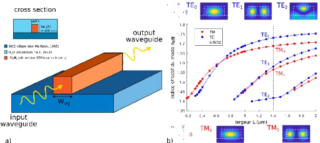
(above). b) Effective indices of the modes and their filed distribution: modes TE0, TE1, TM0 and TM1 are guided modes, as opposed to TM2, which is a radiative mode because its effective index is lower than that of SiO2, represented by a horizontal dashed green line. _________________________________________________ 13 Figure 2.2 Schematics of the working principle for adlayer detection. When the device is exposed to the target molecules, they bond to the molecules locally changing the refractive index. The binding of molecules is comparable to a uniform layer on the waveguide. The presence of the adlayer is converted from speed to intensity using a resonator or an interferometer. ________________________________________________ 14 Figure 2.3: a) Cross-section of a slot waveguide with a material of index. The magnification shows the direction of normal electrical induction at the surface. b) Distribution of the light power in a slotted guide. The maximum intensity of the field is confined to the low index slot which could be, for example, the liquid detection medium. ______________________________________________________________________________________ 15 Figure 2.4 a) Diagram of the mechanism for guiding a surface plasmon-polariton between a dielectric and a metal (in this example gold) b) distribution of the light intensity of an electromagnetic pulse in a surface plasmon waveguide simulated by FDTD method at 1.31 µm. The field is very intense in the dielectric material, for example the liquid medium of interest, while negligible in Au. ___________________________________ 16 Figure 2.5 a) Different geometries of hybrid plasmon guides (image modified to improve readability). b)
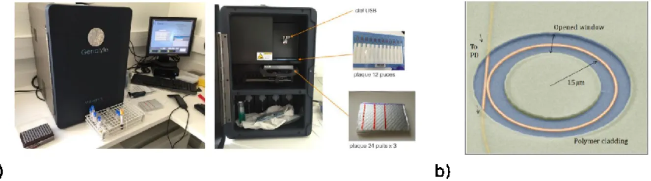
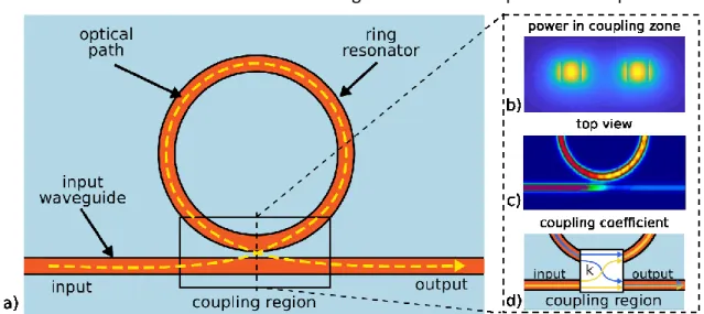
Geometry, cross section and profile of the double-slit hybrid plasmon mode [17]. ______________________ 18 Figure 2.6 Schematic diagram of the Mach-Zehnder interferometer [7] ______________________________ 20 Figure 2.7 a) Diagram of a resonant ring, b) distribution of power in the coupling zone between the bus guide and the ring, c) top view of the light power in the coupling zone and d) coupling diagram between the ring and bus guide _______________________________________________________________________________ 21 Figure 2.8 SEM images of the different resonant ring structures combined with slot guides: a) ring with partial slot [24], b) fully slot ring [7], c) ring and slot bus guide [3]. ________________________________________ 22 Figure 2.9 a) Diagram of the inverted T-slot configuration and b) field distribution in the inverted configuration [25]. ___________________________________________________________________________________ 22 Figure 2.10 a) Plasmonic hybrid waveguide ring: the hybrid mode is formed thanks to the interaction between the waveguides in MoO3 (refractive index 2.06 at 1.55 µm) and MgF2 (refractive index 1.35 at 1.55 µm) and a metallic substrate. Field distribution shows the exponential decay at the sensor edges [4]. b) A double slot resonant ring: the hybrid mode is created between the metal Ag and the Si. The field distribution in the cross-section of the ring shows the strong confinement in the liquid [26]. _________________________________ 23 Figure 2.11 a) Horiba Instruments Surface Plasmon Resonance Imaging, b) SPR Bio Navis, c) Biosensing
Instruments Surface Plasmon Resonance Microscopy ____________________________________________ 26 Figure 2.12 Genalyte detection by ring resonators: a) complete system with the source, detection, microfluidic channels and packaging, b) detail of the ring resonator___________________________________________ 26 Figure 3.1 Dispersion from 1 to 1.7 µm of the real and imaginary part of the refractive index of Au, Cr, SiN, SiO2 and H2O. The solid lines represent the fit and the dots and dashed lines represent the data points respectively. ______________________________________________________________________________________ 34 Figure 3.2 Multilayer structure analyzed by the transfer matrix method: on the left the structure composed of a stack of layers with different dielectric constants along x. Each interface is described by an interface matrix while the homogeneous parts are described by a propagation matrix. _______________________________ 38 Figure 3.3.a, 3.3.c and 3.3.e show the real part of the refractive index along x, perpendicular to the direction of propagation. Figure 3.3.b, 3.3.d and 3.3.f show the absolute value of the normalized Poynting vector, which describes the power distribution of the mode in the different layers for a TE mode. The 𝑛𝑒𝑓𝑓 and the losses for the modes are: 𝑛𝑒𝑓𝑓 = 1.83 and losses = 0 dB/cm for the fundamental mode (figure 3.b), 𝑛𝑒𝑓𝑓 = 1.59 and
losses = 0 dB/cm for the first order mode (figure 3.d) and 𝑛𝑒𝑓𝑓 = 1.36 and losses = 25000 dB/cm for the radiated mode (figure 3.f). _________________________________________________________________ 40 Figure 3.4.a and 3.4.c show the real part of the refractive index along x, perpendicular to the direction of propagation. Figure 3.4.b and 3.4.d absolute value of the normalized Poynting vector for the even and odd modes respectively. Figure 3.4.e plot of the 𝑛𝑒𝑓𝑓 of the isolated, odd and even modes as well as the coupling length of the modes. ______________________________________________________________________ 43 Figure 3.5 Schematic of the interface between two materials and the forward and backward waves in each layer. __________________________________________________________________________________ 45 Figure 3.6 a real part of the refractive index along x. 3.6.b power distribution of the plasmonic mode across the interface, as two decaying exponentials. The effective refractive index is 𝑛𝑒𝑓𝑓 = 1.33 and losses = 554 dB/cm at 1.31µm wavelength. ____________________________________________________________________ 46 Figure 3.7 the error in the convergence test when changing the maximum number of points of the simulation window 𝑛𝑥 𝑚𝑎𝑥. The convergence is reached above 𝑛𝑥 𝑚𝑎𝑥 = 500 which represents the optimal tradeoff between speed and precision. _______________________________________________________________ 48 Figure 3.8.a and 3.8.b show the diagram of the conformal transformation from a conventional waveguide profile to a profile with a conformal transformation. 3.8.c and 3.8.d show the final transformation field
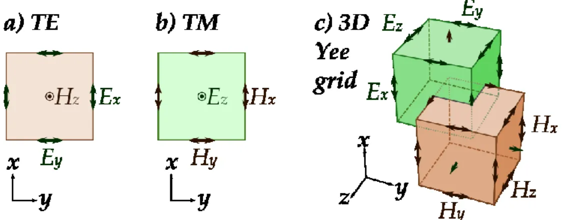
distribution of the mode when the conformal transformation is applied. _____________________________ 49 Figure 3.9 Example of coupling geometry between two waveguides. 3.9.a) top view of two dielectric waveguides A and B in proximity to the coupling region 𝐿𝑖𝑛𝑡. 3.9.b) cross section of the coupling region of the device ___ 50 Figure 3.10.a Plot of the field 𝐸𝑦 of the even mode (𝑛𝑒𝑓𝑓 = 1.558). 3.10.b Plot of the field 𝐸𝑦 of the odd mode (𝑛𝑒𝑓𝑓 = 1.513). _________________________________________________________________________ 50 Figure 3.11.a schematic of the coupling waveguides before and after the discretization. 3.11.b example of interface with the forward and backward waves used for the calculation. ____________________________ 52 Figure 3.12 Yee unit cell for 2D and 3D meshing. It can be noticed that the points for the calculation of the 𝐸 and
𝐻 are shifted. ___________________________________________________________________________ 53
Figure 3.13.a Image of the waveguide, the cross section and 3D view. 3.13.b the 𝑛𝑒𝑓𝑓 as a function of the width of the waveguide. The power distribution for modes at 𝑊𝑤𝑔 = 1.4 𝜇𝑚 are shown. ____________________ 56 Figure 3.14.a example of the geometry of a MMI. b. Image of the power in the 1x2 MMI coupler with the mode matching solver. _________________________________________________________________________ 57 Figure 3.15.a directional coupler schematics,17.b field distribution calculated with mode matching method. _ 58 Figure 3.16 Schematics of a Mach-Zehnder interferometer. The input intensity A+ is split in the two arms of the
interferometer. The arms are asymmetric so when the signals recombine in the output MMI they interfere. The interference is quantified by analyzing the output intensity B+. _____________________________________ 58
Figure 3.17 Different kinds of resonator existing in literature: (a) all-pass circular ring resonator b) all-pass racetrack ring resonator and c) add-drop ring resonator. The parameters are bent radius Rr, width of the loop waveguide Wloop, t dist1 the coupling gap with the waveguide, Wbus the width of the bus waveguide, tdist2 the
coupling gap between the loop and the drop waveguide, Wadd the width of the add waveguide, W drop the
width of the drop waveguide, L1 the horizontal length of the straight part of the racetrack and L2 the vertical length of the straight part of the racetrack. ____________________________________________________ 60 Figure 3.18 racetrack resonator with detail on the coupling section and coupling coefficient 𝑘 and transmission coefficient 𝑡. ____________________________________________________________________________ 61 Figure 3.19 Examples of transmission of a ring resonator with significant parameters. The orange curve is the curve at rest and the blue curve represents a shift due to a refractive index change. ____________________ 63 Figure 3.20.a simplified diagram of the device with the PDMS reservoir walls. The PDMS walls are represented in green, the inside of the pool is the light blue region in the center (the sensing liquid in H2O in this case) and the
outermost regions are air outside the reservoir. 3.20.b example of transmission for a highly perturbed signal with the parasitic interference. The orange circles indicate the parasitic resonances and the blue one the ring resonance peak. _________________________________________________________________________ 65 Figure 3.21.a diagram of the ring resonator with a Fabry-Perrot interferometer in the bus waveguides,
represented by the vertical bars. 3.21.b modified model to include the thickness of the interfaces. 3.21.c result of the model compared to characterization results (the orange curve represents the simulation and the blue one the characterization). _____________________________________________________________________ 66
Figure 3.22 the principle of the back and forward reflections in the PDMS reservoir. Each reflection and
transmission is accounted for up to infinity, as a series. ___________________________________________ 67 Figure 4.2 a) cross-section of the 2 µm waveguide for input butt coupling, b) cross-section of the waveguide for propagation in the photonic chip and c) cross-section of the waveguide for ring resonators’ coupling. ______ 73 Figure 4.2 Schematics of a taper in SiN that ideally goes from Win 2 µm to Wout 0.6 µm. _________________ 74
Figure 4.3 a) MMI geometry and b) simulation by means of the mode matching technique. ______________ 75 Figure 4.4 a) geometry and effective refractive index of 1D dielectric waveguides and the plasmonic
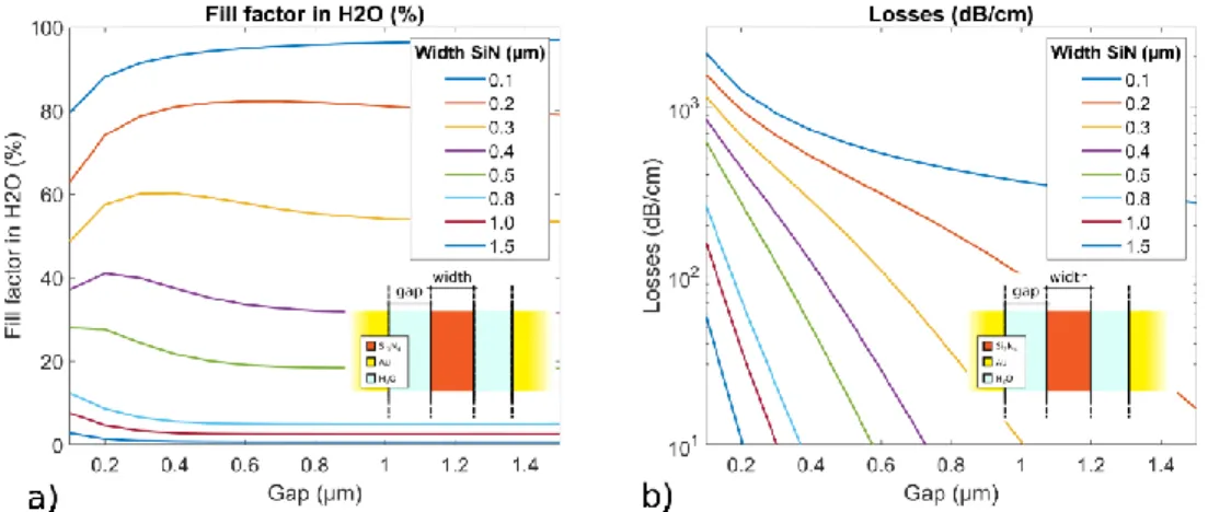
waveguides, b) coupling between two plasmonic waveguides divided in even and odd modes as a function of the distance between the two plasmonic interfaces, c) coupling between the even and odd plasmonic modes and the dielectric mode, also divided between the hybrid even and odd modes. ________________________ 78 Figure 4.5.a) Simulation of the filling factor, i.e. the percentage of the field in the target liquid (water) for different gaps and core widths. b) Losses in dB/cm of the structures for different gaps and core widths. Insets: geometry of the structures. _________________________________________________________________ 79 Figure 4.6 From the 1D simulation to the 2D cross section simulation ________________________________ 80 Figure 4.7 Study of the SiN hybrid waveguide with Au (a) and Al (b). The multiple lines represent different gaps between the metal surface of the plasmonic waveguide and the SiN dielectric waveguide core. The black dotted line shows the 𝑛𝑒𝑓𝑓 as a function of the width of the dielectric waveguide. The red dotted line is the index of the 𝑆𝑖𝑂2, in other words, the limit above which the waveguides support guided modes. _________________ 81 Figure 4.8: Fill factor (a, b), difference of effective refractive index when changing the liquid by one refractive index unit (c, d) and losses in dB/µm (e, f). The red continuous line represents the limit beyond which the hybrid mode is below the cutoff. The purple dashed line represents the limit beyond which the dielectric mode is below the cutoff. (RIU stands for Refractive Index Unit.) _______________________________________________ 82 Figure 4.9 Field distribution of the mode for different geometries: a-b) gap = 100 nm, c-d) gap = 300 nm, e-f) gap = 500 nm, g-h) gap = 1000 nm. When the metal is close to the SiN waveguide, the mode is confined in the gap while, for large gaps, the mode is deconfined towards the substrate. ____________________________ 83 Figure 4.10 Two examples of the desired distribution of power to maximize sensitivity in the case of: a) large molecules and b) small molecules. ___________________________________________________________ 84 Figure 4.11 the study of the sensitivity of the device as a function of the location of a square of biological material with a side of 5 nm. The detection is not done at the surface of the SiO2 but around 5nm above. This can be an advantage because in most cases the target molecules are not located on the surface but on a layer of bio-receptors which is about ten nanometers. ________________________________________________ 85 Figure 4.12 a) Bulk sensitivity of the HPWG ring resonator and b) Q factor as a function of the width of the core waveguide and the gap between the core and the metallic walls ___________________________________ 86 Figure 4.13 Schematics of the hybrid plasmonic ring resonator _____________________________________ 87 Figure 4.14.a) Directional coupler schematic b) field distribution calculated with mode propagation. _______ 87 Figure 4.15 Plan of the complete circuit of the racetrack ring resonator. The parameters chosen for the ring resonator and the MMI are explained in the dedicated sections. All the bend radii are 20 µm. ____________ 89 Figure 4.16: a) Schematics of the device, a racetrack resonator hybridized with Au. The sensitive area is between the SiN waveguide (in orange) and the metallic sides (in yellow). b) Shift of the resonance peak as a function of the gap size and the width of the core waveguide for a racetrack with 20 µm radius bends, coupling length Lcoup
= 10 µm and vertical length Lv = 20 µm. The lines represent the limits beyond which the hybrid mode and the
dielectric mode are below the cutoff. The green dashed box is the area corresponding to the geometry of the fabricated devices in this project. c) Quality factor as a function of the gap and the width of the central waveguide. d) Graph of the minimum detectable shift and the bulk sensitivity as a function of the HPWG percentage occupation of the ring circumference. _______________________________________________ 90 Figure 4.17.a concept of orthogonal differential functionalization to improve high signal in a low concentration regime. 18.b differential functionalization in the article by Palazon, 2015 (scale bar is 100 µm). ___________ 92 Figure 4.18 Model of Bovine Serum Albumin or BSA by Bloomfield. Structure A is the model of the protein divided in a compact core (central dashed part) and a less dense envelope (approximate values of a = 30 nm and b = 3 nm). B, C and D show the spherical model of the protein. _____________________________________ 93 Figure 4.19 adlayer simulations a) when functionalizing Au or b) the dielectrics (SiO2 and SiN). ___________ 94 Figure 4.20 Mach-Zehnder interferometer dimensions of the final design _____________________________ 95
Figure 5.1 Graphic Data System (GDS) of the industrial photolithography mask. a) devices to calculate the losses in the waveguides. b) dielectric part of the HPWG ring with the alignment marks to align the Au plasmonic waveguides. c) Mach-Zehnder interferometer use to experimentally measure the effective refractive index. 101 Figure 5.2 Schematics representing the geometry and the materials of the DAPHNE platform ____________ 102 Figure 5.3 possible geometries of the devices at the end of the industrial fabrication process ____________ 103 Figure 5.4 a) Transmission Electron Microscopy (TEM) image of a SiN waveguide. b) test of reproducibility on the waveguide core layer thickness. _________________________________________________________ 103 Figure 5.5 a) the full wafer and b) the wafer after cleaving with the diamond pen c) after the dicing of the Université de Sherbrooke d) sample from STMicroelectronics. _____________________________________ 104 Figure 5.6 the main steps of the lift-off process from the substrate coming from the STMicroelectronics
cleanroom to the final device with the lift-off. _________________________________________________ 105 Figure 5.7 a) the electron beam microscopy image of the ring resonator before lithography, b) the center of the alignment marks (add the picture of the dielectric waveguide).____________________________________ 107 Figure 5.8 Ellipsometry measurements of a) the real part of the relative permittivity and b) the extinction coefficient k as a function of the wavelength. The curves represent different deposition speeds and the
comparison with the Johnson and Christy data. ________________________________________________ 107 Figure 5.9 fabrication steps associated with the cleanroom images of the process. a) spin-coater, b) the sample inside the scanning electron microscope c) image of the sample after the development. The trapezoidal marks are the hole is the resist. d) The machine for electron beam evaporation Leybold, e) mixer RotoMix type 48200 on which the sample is immersed in acetone, f) final devices with Au patches successfully left of the substrate in correspondence of the holes in the resist. _____________________________________________________ 109 Figure 5.10 Process flow of the CMP method. _________________________________________________ 110 Figure 5.11 Image of the mold for the PDMS and for the sample holder _____________________________ 111 Figure 5.12 a) PDMS mold b) PDMS shaped c) PDMS pool on the sample glued with plasma bonding. _____ 112 Figure 5.13.a image of the microfluidic mold .b Image of the mold glued to the sample ________________ 112 Figure 6.1 a) schematic of the optical set up from the source to the spectrometer b) sketch of the cross section of the stage with the PDMS reservoir and the input and output fibers, c) picture of the setup and the sample. 116 Figure 6.2 Example of two coupling methods on a photonic chip from a fiber: grating coupling in the red square and butt coupling in the blue square_________________________________________________________ 117 Figure 6.3 top view of the chip while injecting and collecting light by the butt coupling method for the input waveguide (left side) and output waveguide (right side). _________________________________________ 118 Figure 6.4 a) Sample holder design with the software Blender b) printed sample holder and sample glued with the PDMS reservoir c) loading the sample with the PDMS reservoir on the sample holder. The two fit together to keep the sample in place __________________________________________________________________ 119 Figure 6.5 a) Microfluidic channel on the sample during the waterproof test in the cleanroom, b) sample on the set up with the input and output channels ____________________________________________________ 120 Figure 6.6 HPWG ring resonator after exposure to glycerol. The residues of organic material stick to the surface, changing the response of the device _________________________________________________________ 121 Figure 6.7 Comparison of Sellmeier and Cauchy equations fitted to the experimental data from Kedengurg 2012. Kedengurg’s data are shown in red and green dots. The fits with Cauchy and Sellmeier are performed only with the data shown in red (0.4µnm – 1µm). Sellmeier equation gives a better estimate at wavelengths outside the fitting range. ___________________________________________________________________________ 124 Figure 6.8 a) example of calibration curve with the error bars along X and Y representing the uncertainty. The dotted red lines represents the uncertainty interval on the fit of the straight line. The slope is the sensitivity. b) Example of transmission curve for different concentrations of analyte, c) zoom on the transmission curve where the blue points are an example of the measurement points, the green curve represents an error on the intensity and the red curve an error on the resonance wavelength. ________________________________________ 126 Figure 6.9 Picture of the cross correlation. The insets show the two functions of which on calculate the cross-correlation. The gray hatched area is the overlap of the two curves. Cross-correlation is proportional to the area of the overlap: when the two curves are perfectly overlapped, cross correlation is maximal. _____________ 128 Figure 6.10 illustrates the FFT method: a) the reference and the measurement spectra and b) transmission spectra after normalization and inversion. c-d) Example of result of the cross-correlation. e-f) Example of the
Figure 6.11.a) schematic of the layout of the device to test linear losses. b) losses in waveguides of different lengths as a function of the wavelength. c) losses (blue) with error bounds (red) as a function of wavelength. _____________________________________________________________________________________ 132 Figure 6.12.a) Transmitted power for the spirals of 700nm width. b) losses (blue) with error bounds (red) as a function of the wavelength ________________________________________________________________ 133 Figure 6.13 transmission of 5 measurements after changing the DI H2O to validate the cleaning procedure and
the procedure to change fluids. The maximum resonance peak change is around 10pm. ________________ 134 Figure 6.14 a. Transmission spectra of the HPWG device for different glucose monohydrate dilutions in H2O. 6.14.b Calibration curve to calculate the sensitivity as the slope of the linear fit of the peak shift as a function of the difference of refractive index of the fluids: “A” represents the reference measurement in pure water, “B”: 2g/100 mL, “C”: 3g/100 mL , “D”: 5g/100 mL and “E”: 6g/100mL. The slope of the fitted line, the sensitivity, is 275 nm/RIU. ___________________________________________________________________________ 135 Figure 6.16 Comparison between simulation with the Jonhson and Cristy Au (Au JC - dark blue bars) and experimental results with peak-search (green) and FFT (light blue) _________________________________ 137 Figure 6.15 cross section of the three considered samples with the gap measured at the Electron Scanning Microscope. ____________________________________________________________________________ 137 Figure 6.17.a) image of the AFM tip, inclination of 20°. b) Cross section of the simulated waveguides. c) Average profile over a SiN waveguide. ______________________________________________________________ 138 Figure 6.18 comparison of the sensitivity for simulated devices and the experimental results for three samples, PR22_4G, PR23_4G and PR12_10P. _________________________________________________________ 139 Figure 6.19 simulation of the losses of three samples, PR22_4G, PR23_4G and PR12_10P, with different types of Au and Cr. The Cr and the Au INL both contribute to increase losses. _______________________________ 140 Figure 6.20 Experimental sensitivity of the resonators for two SiN waveguide widths and two configurations (Au INL slow deposition compared with the ring resonators without Au). _______________________________ 141 Figure 6.21 schematic of differential functionalization for thiols, streptavidin, biotin and nanoparticles with rhodamine and the different estimated thicknesses _____________________________________________ 143 Figure 6.22 result of the differential functionalization. a) image of the fluorescent light, b) image of the visible light where the lighter part is the Au, superposition of the two where the red points are the fluorescent light of the nanoparticles. _______________________________________________________________________ 144 Figure 6.23 Mach-Zehnder interferometer - comparison between the experimental results (red curve) and the nonlinear fit (blue curve). The inset shows the cross section of the waveguide.________________________ 145 Figure 7.1 schematic of an improved plasmonic waveguide configuration for a more efficient functionalization _____________________________________________________________________________________ 151 Figure 7.2 a) setup where neither the source nor the detection are integrated, b) setup where the detection is integrated, c) setup where both the source and the detection are integrated. ________________________ 152 Figure A.1 Process flow of the CMP method. __________________________________________________ 155 Figure A.2 schematic of the ICP etching ______________________________________________________ 155 Figure A.3.a side view of the etched patch. We can notice that there is no more resist present that the
roughness is rather high. A.3.b Side view of the etched patch _____________________________________ 156 Figure A.4.a schematics of the deposition process. A.4.b-d SEM cross-sections of depositions at different angles (θ = 20°, θ = 30° and θ = 45°). ______________________________________________________________ 157 Figure A.5 Result of the CMP of one ring resonator and one Au patch. The pictures were colored to underline the different materials. The yellow is the Au and the orange is the SiN while the rest is SiO2. ________________ 158
Figure A.6 etching rate. Each point is an average of three SEM measures. The calculated etching time is 110 nm/min _______________________________________________________________________________ 158 Figure B.1.a single mode bus waveguide and mode profile. 1.b two-mode waveguide where the first order mode profile is shown (effective index is 1.45, close to the cutoff). 1.c shows the two waveguides close to each other and the coupling between the two modes. ____________________________________________________ 160 Figure B.2 Scanning electron microscope image of the higher order mode ring resonator. A zoom on the
coupling section is shown as well as the schematic showing the cross section. ________________________ 160 Figure B.3.a transmissions spectra for the higher order mode device for different glucose monohydrate dilutions in H2O. 3.b Calibration curve to calculate the sensitivity as the slope of the linear fit: “A” represent the reference
Figure R1.1 Schéma du fonctionnement d’un biocapteur : deux composantes principales (le test biochimique et le transducteur) qui donnent comme résultat un signal mesurable. ________________________________ 163 Figure R1.2 Schéma du fonctionnement de la détection de surface. ________________________________ 164 Figure R1.3 a) Schéma d’un guide d’onde avec un cœur de Si3N4 et une gaine composée en partie par du SiO2 et
de l’H2O. b) Distribution des modes et leur cartographie de champ : les modes A, B, D et E sont des modes
guidés, par opposition à C qui est un mode radiatif car son indice effectif est inférieur celui du SiO2, représenté
par une ligne horizontale verte sur la figure. __________________________________________________ 167 Figure R1.4 : a) Schéma d’un guide fente avec un matériau d’indices de réfraction n1 > n2. L’agrandissement montre la direction de l’induction électrique normale la surface. b) Distribution de la puissance lumineuse dans un guide fente. L’intensité maximale du champ est localisée dans la fente de faible indice de réfraction qui pourrait être, par exemple, le milieu liquide de détection. ________________________________________ 168 Figure R1.5 a) Schéma du mécanisme de guidage d’un plasmon-polariton de surface entre un diélectrique et un métal (dans cet exemple de l’or) b) Distribution de l’intensité lumineuse d’une impulsion électromagnétique dans un guide plasmon de surface. Le champ est très intense dans le matériau diélectrique, par exemple le milieu liquide d’intérêt, près de l’interface métal/diélectrique et négligeable dans l’or. La simulation a été faite avec un moteur FDTD à = 1.31µm. _________________________________________________________ 169 Figure R1.6 a) Différentes géométries de guides d’onde plasmonique hybrides (image modifiée pour améliorer la lisibilité) [1], b) Géométrie, coupe transversale et profil du mode guidé double fente hybride plasmonique [23]. _____________________________________________________________________________________ 170 Figure R1.7 Schéma d’un interféromètre Mach-Zehnder utilisé comme capteur [7]. ____________________ 172 Figure R1.8 a) Schéma d’un anneau résonant, b) distribution de la puissance dans la zone de couplage entre le guide bus et l’anneau, c) vue de dessus de la puissance lumineuse dans la zone de couplage et d) schéma de couplage entre l’anneau et le guide bus ______________________________________________________ 173 Figure R1.9 Images MEB des différentes structures en anneau résonant combinées avec des guides d’onde à fente : a) anneau avec une portion de guide d’onde à fente [21], b) anneau totalement à fente [24], c) anneau et guide d’onde bus à fente [11].______________________________________________________________ 174 Figure R1.10 a) Schéma de la configuration fente en T inversé et b) distribution de champ dans la configuration inversée [12]. ___________________________________________________________________________ 174 Figure R.11 a) Anneau guide hybride plasmonique : le mode hybride est formé grâce à l’interaction entre les guides en MoO3 (indice de réfraction de 2.06 à = 1.55µm) et MgF2 (indice de réfraction de 1.35 à = 1.55µm)
et un substrat métallique. La cartographie de champ montre le profil exponentiel en surface du capteur [16], b) un anneau résonant double slot : le mode hybride est créé entre le métal Ag et le Si. La distribution de champ dans la section de l’anneau montre le fort confinement dans le liquide [22]. _________________________ 175 Figure R1.12 Exemple de la géométrie d’un résonateur en anneau et de sa transmission _____________ 180 Figure R1.13 a) Schéma de la coupe transversale du guide d’onde et de la distribution de la puissance lumineuse calculée par l’outil de calcul de modes (W = 300nm, h = 600 nm, gap = 300 nm). b) Schéma du dispositif en 3D avec les interactions biologiques. Le rayon de courbure des virages est de 20µm, assez grands pour considérer les pertes nulles dans ces zones. ____________________________________________________________ 182 Figure R1.14 Processus d’optimisation des paramètres géométriques selon les besoins de performances. __ 183 Figure R1.15 Etapes de fabrication du proceed Lift off illustrées par des images prises en salle blanche durant la réalisation. a) dépot de la résine à la tournette, b) Lithographie électronique c) image d’un échantillon après le développement. Les papillons trapézoidaux représentent les trous dans la résine. d) Evaporation du metal par canon à electron Leybold, e) Lift off dans le mixer RotoMix type 48200 où l’échantillon est immergé dans l’acétone, f) Echantillon en fin de procédé. ____________________________________________________ 185 Figure R1.16 a) Vue en coupe du guide de Nitrure de Silicium. b) Différence entre couplage par réseau de diffraction et couplage par la tranche c) Schéma du montage optique. ______________________________ 187 Figure R1.17 Banc de caractérisation a) Synoptique du banc de caractérisation b) Schéma du banc de
caractérisation avec la partie microfluidique c) photographie du banc de caractérisation et du réservoir en PDMS _________________________________________________________________________________ 189 Figure R1.19 Etude comparative de la sensibilité du dispositif entre les simulations en considérant l’indice de réfraction de l’Au Jonhson et Cristy (bleu foncé barres d’erreurs en noir) et les résultats expérimentaux obtenus avec les méthodes peak-search (vert) and FFT (bleu clair) ________________________________________ 191
Figure R1.18 cross section of the three considered samples with the gap measured at the Electron Scanning Microscope. ____________________________________________________________________________ 191 Figure R1.21 Simulation des pertes de propagation des 3 échantillons PR22_4G, PR23_4G et PR12_10P, pour différentes configurations Au. Au INL dépôt rapide, Au+Cr et Au+Cr INL dépôt rapide. L’ajout de la couche d’accroche de Cr et la porosité induit par le dépôt rapide induisent un surcroit de pertes de propagation. __ 193 Figure R1.20 comparison of the sensitivity for simulated devices and the experimental results for three samples, PR22_4G, PR23_4G and PR12_10P. _________________________________________________________ 193 Figure R1.22 Sensibilité mesurée pour différents résonateurs avec 2 largeurs de guides d’onde SiN et avec ou sans Au. _______________________________________________________________________________ 195
List of tables
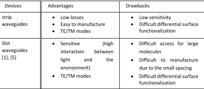
Table 2.1 Waveguides for Integrated Photonic Detection: Benefits and disadvantages __________________ 18 Table 3.1 Dispersion formulae for the real part of the refractive index of SiO2, SiN and H2O _______________ 34
Table 3.2 The simulation methods included in this thesis __________________________________________ 54 Table 4.1 Metals available at STMicroelectronics and their characteristics that helped to choose the most appropriate metal: the plasmonic behaviour in the infrared, the compatibility with the biology test existing and the compatibility with nano-patterning fabrication constraints. ____________________________________ 76 Table 4.2 Dimensions of the BSA protein in different studies [24] ___________________________________ 93 Table 6.1 Advantages and drawbacks of each method __________________________________________ 120 Table 6.2 Coefficients of thermal expansion for SiN, Au and SiO2 ___________________________________ 125
Table 6.3 Advantages and drawbacks of the two main methodologies ______________________________ 130 Table 6.4 Table of uncertainty along the horizontal and vertical axis _______________________________ 131 Table 6.5 comparison of the coefficients of the fitting 𝑛𝑒𝑓𝑓 model found by theoretical simulation and the experimental values found with the nonlinear fit. ______________________________________________ 146 Table A.1 Parameters of the ICP etching recipe Si3N4_T _________________________________________ 156 Tableau R1.1 Guides d’onde pour la détection photonique intégrée : avantages et inconvénients _________ 170
AKNOWLEDGEMENTS
A Ph.D. is a complicated and demanding journey and this one was not an exception. This project could not be completed without the constant help of the people surrounding me. I would like to be able to thank all of you on this short page but unfortunately, the space is limited so I will limit myself to the people with whom I spent more time but all of you are in my memory.
I would start thanking my supervisors Regis Orobtchouk, Paul Charette and Stephane Monfray for believing in me from the beginning. Thank you for your patience and for being there when I needed you. I would also like to thank Michael Canva and Pedro Rojo Romeo for the many fruitful discussions as well as and Frederic Boeuf for believing in me.
My first year was in Lyon so I will start with the people who helped me the most there. Thank you, Tulio, Thais, PV, Prabir, Remi, Nicolas, Florian, Ali, Malik, Jeremy, Florian, Tom, Jordan, Anais, Alberto, Eirini, Samir, Jimmy, Solene, Annie, Virginie, Maurin, Greta, Jeremie, Sarah, Seif, Eva, Paul, Marco, Getenet, Remi, Pierre, Raphael, Panthea, Kokou, Remi, Maxime, Amalric, Sylvain and Sebastian. Thank you for the time you took to talk and listen to me and thank you for your technical and moral support. I would also like to thank the staff of the cleanroom and the beautiful people who started with me the Student Chapter.
I then went to Sherbrooke. At first, I would like to thank Guillaume Beaudin for all the time, patience and for your bright and always spot-on suggestions. Thank you to all the colleagues that, despite the cold Canadian winter, managed to warm this experience even in the coldest moments. Thank you Marine, Stephanie, Marion, Jean-Francois, Ulrike, Yann, Valerie, Olivier, Fanny, Quentin, Tigran, Arthur, Zhor, Maxime, Clement, Pedro, Gwénaëlle, Alexandre, Frederic, Gwénaëlle, Julien, Romain, Guillaume, Abdelatif, Laurence, Marie-Josée, Laurence, Pauline, Etienne, Felix, Adham, Daniel, Caroline, Serge, Marina, Emmanuel, Regis, Mikel. Thank you as well to all the members of the CASS for this great experience.
I cannot forget the help of the team of friends with whom I shared the passion of Lindy Hop, Rockabilly Jive and “Fakecoast”. Thanks to you I was able to turn on the light even in the darkest of times. Thank you, Jessica, Celine, Carlos, Maria, Myrtho, Anika, Elodie, Scott, Andrée-Anne, Alexandre, Jessica, Josée, Jean-Francois, Marianne, Marie-Eve, Marc, Mercedes, Kenza, Cora, Yoanna, Aurelien. Thank you for your unconditioned affection. Thank you to the friends of the “maison jaune” that kept me young during my stay in Canada. A special thank you to Christiane because living with you was an incredible experience. Thank you for making me discover how amazing people can be. Thank you for the meals together, for the many discoveries and unforgettable discussions.
Thanks to Michael and Natacha for always taking care of me, in particular during the hardest moments. I will never forget all the delicious hot meals to cheer me up after a particularly difficult day.
Volevo ringraziare inoltre gli amici di lunga data che mi hanno sostenuto nonstante la distanza. Grazie al gruppo dei Tacchini per il sostegno sempre e comunque. Grazie a Stefano e Lara, per le risate a crepapelle. Grazie a Stefano e alle sue amiche per il sostegno soprattutto all’inizio di quest’avventura.
Un enorme grazie alla mia famiglia che mi ha seguito passo a passo, che ha condiviso le mie vittorie e le sconfitte. Grazie per avermi sostenuto durante questa esperienza. Grazie mamma, papa, Paola e Saverio per avermi ancora una volta fatto vedere che siete la più bella famiglia che potessi avere. Vorrei ringraziare di cuore anche Elia e Gino per il magico aiuto sempre presente, anche da molto lontano. Grazie a zia Silvia, zio Mario, Chiara, Giulio e Edo per il vostro affetto incondizionato.
To conclude, I would like to thank Jaime for always supporting me with a smile, for cheering me up and listening when things were complicated. Thank you for your bright and inspiring personality that taught me so much.
CHAPTER 1 - INTRODUCTION AND CONTEXT
The detection of biological molecules is of major interest in different fields: from public health to food quality control, from animal nutrition to military defence [1]—[6]. Biosensors were invented roughly 60 years ago (the first publication in 1962 [7]) to answer these needs. The success of biosensors is well known in literature and it is marked by great success such as the glucose pen and the electronic nose [8], [9].
More precisely, a biosensor consists of a transducer converting the phenomenon of interest into a measurable signal, as shown in Figure 1.1. Based on the application of the sensor, the phenomenon can range from the presence of a molecule in a complex medium to the dynamic of a reaction. The transducer converts the result of the biochemical test into an (often electrically) measurable signal. The signal is compared to the calibration curve of the sensor, representing the standard values of the sensor response. In this way, the information about the analyte (or target molecule) is determined.
One of the main objectives of a biosensor is to optimize its sensitivity. However, there is more to this: based on the application, a biosensor needs to be small and affordable to successfully help users, reducing the volume of the material under analysis and making analysis on site possible [10]. These systems are equivalent to an analysis laboratory integrated in a hand-held device. This is why they are referred to as lab-on-a-chip or lab-on-chip or LOC [11]. Such a system is by definition heterogeneous, because it integrates several domains, such as electronics, photonics, microfluidics and biology. This is why they appeared around the 1980s and ’90s when thin-film technology allowed the production of miniaturized micro pumps, flow sensors and integrated fluidic systems [12], [13].
Figure 1.1 The schematic principle of a biosensor for detection of analytes. The analyte interacts with the bioreceptor to change the measured signal. The transducer converts the
analyte presence in a change of the measurable signal. After results’ post-processing, the biosensor main properties are extracted (e.g. sensitivity, limit of detection).
1.2 OBJECTIVES
The long-term goal of this work is to build a LOC system, focusing on four main goals: sensitive biological transduction, compatible with industrial manufacturing (which provides large volumes at low cost), compact and versatile for different biological targets.
This PhD project is the result of a collaboration between three entities: the Institut National
des Sciences Appliquées de Lyon (INSA de Lyon), the Université de Sherbrooke and
STMicroelectronics. The participation of an industrial partner to the project constitutes a realistic example of a mass production environment.
1.2.1 RESEARCH QUESTION
The research question at the heart of this research is the following:
How to design, manufacture and test a compact biosensor based on integrated photonic transduction, simple to functionalize, compatible with an industrial platform and lab-on-chip, having a sensitivity comparable or higher than the state of the art?
In other words, the objective of this doctorate is to identify and assess the potential of an integrated photonic transducer compatible with LOC characteristics. Therefore, throughout this work the choices of the device parameters (e.g. materials and geometry) are done taking into account their compatibility with industrial and LOC constraints. In such a multidisciplinary context, it is fundamental to consider all the perspectives to have a realistic candidate, easy to convert into a potentially commercializable product.
After deciding the most adequate device based on literature, its potential is assessed by simulation, manufacture and characterization. As explained in the next chapter, the transducer considered in this study is a ring resonator based on a dielectric-metal hybrid waveguide, also known as Hybrid Plasmonic Waveguide or HPWG. The literature shows that HPWG devices are sensitive, compatible with chemical functionalization, versatile and compatible with industry manufacturing, thus a good candidate for the LOC application. As stated before, 4 factors are taken into consideration when choosing and designing the device:
The photonic transduction must be chosen to allow specific detection of the target molecules and a measurable signal at the output.
From a biological standpoint the molecules of interest must be able to reach the detection zone. Furthermore, analytes should be encouraged to occupy preferentially the detection zone other than the other “dead” zones of the device. Therefore, the detection zone must be accessible for target molecules and adapted for differential chemistry.
For the microfluidic part, the substrate used must be compatible with a bonding of microchannels produced for example with polydimethylsiloxane or PDMS, a polymer often used in microfluidics. LOC rely on these type of channels to manipulate complex solutions.
![Figure 2.9 a) Diagram of the inverted T-slot configuration and b) field distribution in the inverted configuration [25]](https://thumb-eu.123doks.com/thumbv2/123doknet/3314236.95456/42.892.112.783.334.473/figure-diagram-inverted-configuration-field-distribution-inverted-configuration.webp)