Research Article
Gold Nanorods Incorporated Cathode for Better Performance of
Polymer Solar Cells
Alaa Y. Mahmoud,
1,2,3Ricardo Izquierdo,
2and Vo-Van Truong
11Department of Physics, Concordia University, Montr´eal, QC, Canada H4B 1R6
2D´epartement d’Informatique, Universit´e du Qu´ebec `a Montr´eal, Montr´eal, QC, Canada H3C 3P8 3King AbdulAziz University, P.O. Box 80200, Jeddah 21589, Saudi Arabia
Correspondence should be addressed to Vo-Van Truong; [email protected]
Received 26 September 2013; Revised 21 November 2013; Accepted 21 November 2013; Published 29 January 2014 Academic Editor: Ji Sun Im
Copyright © 2014 Alaa Y. Mahmoud et al. This is an open access article distributed under the Creative Commons Attribution License, which permits unrestricted use, distribution, and reproduction in any medium, provided the original work is properly cited.
The effect of inserting low density of gold nanorods in the metallic rear electrode of polymer solar cells on their performance was studied. Gold nanorods were introduced by spin-coating their aqueous solution directly on top of the
poly(3-hexylthiophene-2,5-diyl):[6,6]-phenyl-C61-butyric-acid-methyl-ester layer. The resulting devices showed a 5% increase in the short circuit current that
leads to a 14% enhancement in the power conversion efficiency. Investigation on the photocurrent spectral response of devices with/without gold nanorods revealed that incorporating the rods helped in enhancing the devices photogenerated current near the plasmonic absorption modes of the rods. The enhancement in the devices efficiency is related to the increase in their absorptivity due to the far-field and near-field effect of localized surface plasmon resonance induced by the presence of the rods in the interface between the photoactive layer and the metallic rear electrode.
1. Introduction
Intensive research has been dedicated to enhancing the power conversion efficiency (PCE) of organic solar cells (OSCs) due to their attractive features such as solvent solubility,
portability, flexibility, and low cost, [1–4]. Up to now, the
PCE of bulk heterojunction (BHJ) polymer solar cells made by the blend of the polymer
poly(3-hexylthiophene-2,5-diyl) (P3HT) and the fullerene-derivative[6, 6]-phenyl-C61
-butyric-acid-methyl-ester (PCBM) has reached ∼5% [5].
Unlike their inorganic counterparts, the absorption of light in organic materials creates bounded electron-hole pairs (excitons) with a short diffusion length rather than the free charge carriers. Thereby, the photoactive layer in OSCs has to be in the range of a few hundred nanometers of thickness to limit the recombination of the charge carriers. Such thin photoactive film allows for more transmission loss of the
incident light [2,4].
To overcome the absorption loss in thin-film photovoltaic (PV) devices, the optical path length of the incident light inside the absorber has to be enlarged without increasing
the absorber thickness [6–8]. This could be achieved by
uti-lizing the light trapping mechanism associated with excited plasmonic particles. Plasmonic phenomenon in illuminated metallic nanoparticles (MNPs), such as gold and silver MNPs, occurs when the oscillations of the incident electric field resonate with the ones of the electronic charge in the surface of MNPs. Such resonance allows MNPs to absorb light in the visible region of the spectra, leading to intensification, by a factor of 100, in the electromagnetic (EM) field surrounding
them [5]. Metallic nanoparticles are widely used in thin-film
solar cells to enhance their absorption of light by utilizing the far-field and near-field effect associated with their localized
surface plasmon resonance (LSPR) [9–15].
Although various shapes of gold nanoparticles support the LSPR, the scattering cross-section of particles with a cylindrical shape, however, is much larger than the one
associated with the spherical particles [16]. This motivated
the use of the rod shape of gold nanoparticles in the current work. In previous works we investigated the effect of inserting gold nanorods (Au NRs) into P3HT:PCBM BHJ-OSCs by depositing them on the anodic layer, indium tin oxide (ITO)
Volume 2014, Article ID 464160, 7 pages http://dx.doi.org/10.1155/2014/464160
[14] or the photoactive one [18].
In spite of the fact that the fraction of the backward scattered light into the cell (from MNPs placed on the cell’s rear electrode) is comparable to the forward scattered one (from MNPs placed on the front electrode), it has been reported that placing the MNPs on the cell’s rear electrode is
preferable to having them in the front one [19]. This is due to
the fact that the loss in the absorption of light at wavelengths with energies higher than the energy of surface plasmon is prevented by limiting the destructive interference between the scattered and unscattered light, while light at lower energy
gets coupled inside the cell [6,19,20]. Furthermore, placing
the particles in contact with the photoactive layer makes it possible for the intensified EM field around them to reach the photoactive film and excite more charge carriers. In addition, MNPs in the photoactive layer introduce quenching energy states for the excitons, which reduces the number of free
charges carriers that are collected by electrodes [11, 12,18].
These points suggested that having the Au NRs on top of the photoactive layer would lead to better increases in both EM field and the optical path length of the incident light inside the absorber. In addition, there have been no previous studies on the effect of depositing MNPs in contact with the polymer solar cell’s cathode.
In the this study, we report on the effect of incorporating gold nanorods into the rear electrode of BHJ-OSCs on their overall performance by spin-coating many layers of Au NRs directly on top of the P3HT:PCBM film. The investigation on the spectral response of the resulting photogenerated current from devices with/without Au NRs revealed that the photogenerated current for devices incorporating Au NRs was enhanced near the plasmonic absorption modes of the rods. The presence of Au NRs on top of P3HT:PCBM layer would induce more trapping and intensification of the incident EM in the photoactive layer. This thereby will enhance the film absorptivity to the incident light, leading to improved overall performance of the devices.
2. Experimental Methods
Poly(3,4-ethylenedioxythiophene):poly(styrenesulfonate) (PEDOT:PSS) (CLEVIOS P VP AI 4083) was purchased from HC Stark. P3HT with a high regioregularity (98%) and
an average molecular weight<50,000 MW was purchased
from Rieke Metals. PCBM (>99.5%) and 1,2-dichlorobenzene (anhydrous, 99%) were purchased from Sigma-Aldrich. The materials were used as received without further purification. Gold nanorods in an aqueous solution were obtained from the Institut National de la Recherche Scientifique at Varennes (INRS-EMT). Details about preparation of Au NRs
were mentioned in [17]. The concentration of Au NRs in the
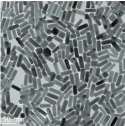
aqueous solution was∼1.593 × 10¹²rods/mL. Figure1shows
the transmission electron microscopy (TEM) image of the rods, which reveals that the ratio between rods’ long and short axes is around 4.
For device fabrication, the P3HT:PCBM blends at a 1 : 0.8 ratio were prepared inside a nitrogen-filled glovebox by
Figure 1: TEM image for Au NRs reveals that the aspect ratio is∼4.
separately dissolving 20 mg of P3HT and 16 mg of PCBM in 1 mL of 1,2-dichlorobenzene. Equal volumes of P3HT and PCBM solutions were then mixed together and stirred overnight at room temperature to ensure more homogene-ity. Prepatterned/cleaned ITO-coated glass substrates were subjected to an oxygen plasma treatment before spin-coating
PEDOT:PSS solution after passing it through a 0.45𝜇m
PVDF filter. The ITO/PEDOT:PSS substrates were baked
at 120∘C for 1 h and then transferred to the nitrogen-filled
glovebox for the deposition of the photoactive layer. The photoactive film P3HT:PCBM was spin-coated on top of the modified ITO/PEDOT:PSS electrodes after being passed
through a 0.45𝜇m PTFE filter. Substrates were then left to
dry in a covered petri dish for 30 min. Afterwards, various Au NRs layers (1, 3, and 5) were directly spin-coated on top of the photoactive film. The spin-coating of Au NRs was performed using a two-step process, first at a slow speed of 200 RPM for 3 sec and then at 1000 RPM for 10 sec. Substrates were then
annealed at 150∘C for 30 min to be dehydrated. The device
fabrication was completed by evaporating a LiF/Al bilayer
cathode under pressure less than10−6torr to yield substrates
with devices having an active area of 0.16 cm2/each. The final
configuration of the Au NRs incorporated device is presented
in Figure2along with the chemical formulas of both P3HT
and PCBM materials.
3. Characterizations
OSC devices were characterized under ambient condition without any encapsulation, in which they were placed under-neath the UV solar simulator lamp (xenon lamp,Oriel Instru-ments) that was equipped with AM 1.5 G filer. The output
intensity of the lamp was adjusted to 100 mW/cm2 using
a silicon photodiode (LI-200 Pyranometer). The
current-voltage(𝐽𝑉) measurements were carried out using a
source-meter (Keithley 2400). The PV parasource-meters, open circuit
voltage (𝑉oc), short circuit current (𝐽sc), fill factor (FF), and
PCE, were measured in devices with and without Au NRs that were made under the same experimental conditions.
Glass ITO PEDOT:PSS P3HT:PCBM Au NRs LiF/Al (a) S P3HT O PCBM C6H13 OCH3 (b)
Figure 2: The final configuration of our OSC devices with Au NRs deposited on top of the photoactive layer; and the chemical formulas of both p3HT and PCBM. 0 0.1 0.2 0.3 0.4 0.5 0.6 0.7 0.8 0.9 1 360 410 460 510 560 610 660 710 760 Au NR solution P3HT:PCBM film Wavelength (nm) N o rm alized a b so rba n ce
Figure 3: Spectra comparison between Au NRs solutions along with the spectra of P3HT:PCBM film.
Since our devices were exposed to air at a certain point during evaporation and characterization processes, the values of PCE were generally low. For analyzing data and scientific visualization solution, the Qtiplot program was used in which the error bars were determined.
The photocurrent spectral response measurements of the devices were carried out by varying the wavelengths of the incident light from 400 nm to 800 nm using a Newport 74000 monochromator.
The optical properties of both Au NRs and P3HT:PCBM were studied using a UV-Vis spectrophotometer (Perki-nElmer LAMBDA 650 spectrophotometer). The surface structure of the resulting Au NRs layers was characterized using a scanning electron microscopy (FEG-SEM Hitachi S-4700), in which the density of the rods in the layer was determined.
4. Results and Discussion
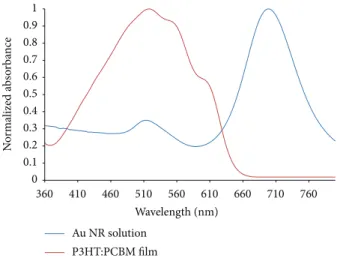
Figure3illustrates the normalized absorption spectra for Au
NRs solution along with the spectra of the P3HT:PCBM film. The blue curve for Au NRs solution shows two peaks of their
Figure 4: SEM image for a layer of Au NRs spin-coated on ITO-coated glass. The white droplet-like indicates the rods. The background is the ITO. The bar indicates 500 nm.
resonance modes, transverse and longitudinal, respectively, located at 540 nm and 740 nm. The red curve shows that the absorption of the P3HT:PCBM photoactive film ranges from 370 nm to 650 nm, with an absorbance maximum around 518 nm and two shoulder peaks around 560 and 610 nm. This
absorbance profile is due to the𝜋-𝜋∗ electronic transitions
between 0-1 and 0-0 spin states for the maximum and the
shoulder peaks, respectively [21, 22]. It is clear that the
position of the transverse absorption peak of the rods is associated with the absorption maximum of the P3HT:PCBM film. Besides, the longitudinal absorption peak of the rods is close to the IR absorption edge of the photoactive film. Hence, the intensified EM field around Au NRs would increase the absorption of the photoactive film near the plasmon peaks of the rods, in which an enhancement in the film absorption
near the IR region is expected [14,18].
To compare both of the microscopic and spectroscopic properties of the deposited Au NRs layers, one, three, and five layers of Au NRs were separately spin-coated on
ITO-coated glass. The SEM images in Figure 4 show that such
spin-coating deposition of many layers of Au NRs produced rods with various densities and arbitrary alignments on the substrate. Accordingly, the spectral measurements of the
obtained 1, 3, and 5 rods layer(s), illustrated in Figure5, were
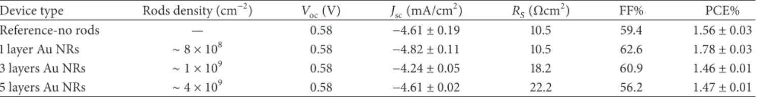
standard deviation.𝑅𝑆was extracted from the inverse of the slope of the JV characteristics in the dark condition at 0.8 V.
Device type Rods density (cm−2) 𝑉oc(V) 𝐽sc(mA/cm2) 𝑅𝑆(Ωcm2) FF% PCE%
Reference-no rods — 0.58 −4.61 ± 0.19 10.5 59.4 1.56 ± 0.03 1 layer Au NRs ∼ 8 × 10⁸ 0.58 −4.82 ± 0.11 10.5 62.6 1.78 ± 0.03 3 layers Au NRs ∼ 1 × 10⁹ 0.58 −4.24 ± 0.05 18.2 60.9 1.46 ± 0.01 5 layers Au NRs ∼ 4 × 10⁹ 0.58 −4.61 ± 0.02 22.2 56.2 1.47 ± 0.01 0 0.002 0.004 0.006 0.008 0.01 0.012 400 450 500 550 600 650 700 750 800 1 layer of Au NRs 3 layers of Au NRs 5 layers of Au NRs Wavelength (nm) A b so rba n ce
Figure 5: UV-Vis spectra for 1, 3, and 5 layers of Au NRs spin-coated on top of ITO-coated glass. The differences in the absorption profiles of the layers are due to the difference in the densities and alignments of the rods on the substrate.
at the ITO surface explains the appearance of the two peaks in the spectrum. A more intense peak is observed for the five-layer deposit, which produced denser rods in the layer
(∼4 × 109cm−2). For one and three layers of rods, the particles
densities were∼8 × 10⁸and1 × 109cm−2, respectively.
To examine the effect of incorporating Au NRs on top of the photoactive layer of the OSC devices, the PV parameters of fully fabricated devices with/without rods were measured
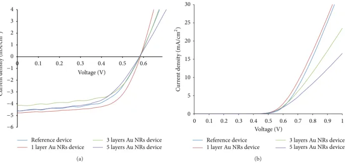
and compared. Figure 6 illustrates the 𝐽𝑉 curves under
illumination and in dark conditions for reference device along with devices incorporated Au NRs on top of the
pho-toactive layer, and Table1 summarizes their corresponding
PV parameters. As Table1shows, depositing the Au NRs on
top of the P3HT:PCBM film increased the𝐽sc by up to 5%
which succeeded in enhancing the PCE by up to 14.1% for devices incorporating one layer of Au NRs. However, devices with 3 and 5 layers of the rods on top of the photoactive layer showed a slight decrease in the PCE. The increase in the device performance via incorporating a layer of the rods in contact with the cell’s back electrodes could be explained by the following mechanisms: the EM field associated with the LSPR of Au NRs (near-field effect) was intensified near the photoactive layer, or the optical path length of the incident
light inside the photoactive layer was increased due to the backward scattering (far-field effect) of the incident light
[5,6,19]. Both mechanisms will result in intensification of the
incident light inside the P3HT:PCBM layer, leading to better generation of the charge carriers in the photoactive layer. This
would cause the increase in the𝐽scand the enhancement in
the PCE of the resulting device.
Figure7(a)shows the spectral measurements of the
pho-togenerated current density for reference device along with the one that incorporated a layer of Au NRs on top of the pho-toactive film. The photocurrent measurements give a picture of the photogenerated charge carriers upon light illumination
[20]. It is obvious that the𝐽scwas enhanced by the deposition
of the rods layer. To study the effect of the multimodes exci-tation of the nanorods on the photogenerated current density
before (𝐽Re) and after (𝐽NR) incorporating one layer of Au
NRs on the cell’s rear electrode, we investigated in Figure7(b)
the spectral measurements of the ratio𝐽NR/𝐽Re along with
the spectrum of Au NRs solution. Since the absorption of our photoactive film does not exceed 650 nm, there was a decrease in the enhancement of the photogenerated current
around 680–760 nm. As Figure7(b)depicts, the𝐽Reenhanced
by 1.13-, 1.14-, and 1.16-folds, respectively, at 460, 640, and
670 nm. These remarkable enhancements in the𝐽Reare near
the transverse absorption mode of the Au NRs and the tail of the longitudinal one, respectively, considering the probability of shifting the absorption maxima for Au NRs with changing
the surrounding environments. The increase in the𝐽Recould
be related to the increase in the generated free charge carriers in the photoactive film due to the backward scattering process from the rods, or the intensification of the EM field surround-ing them. Although there was no large enhancement in the absorption profile of the P3HT:PCBM/AuNRs films near the
IR region, a very small increase in the𝐽Rewas observed at this
region, particularly at 670–700 nm, which can be attributed to the longitudinal absorption mode of Au NRs. Hence, we suggested that the photogeneration of excitons near the transverse and longitudinal absorption modes of Au NRs was enhanced, which improved the total device efficiency. Our results are somewhat similar to those obtained by Chen
et al. [15] who reported on enhancements in organic cells
with gold nanofilms thermally evaporated in vacuum onto a LiF/Al electrode. Their results showed an enhancement in the
𝐽NR/𝐽Reratio near the absorption profile of nanotextured Au
thin films.
For more than a layer of the rods on the P3HT:PCBM
film,3- and 5-layer cases, as presented in Table1, there was
a reduction in the values of both𝐽sc and PCE as compared
0 1 2 3 4 0 0.1 0.2 0.3 0.4 0.5 0.6 Reference device 1 layer Au NRs device 3 layers Au NRs device 5 layers Au NRs device Voltage (V) −6 −5 −4 −3 −2 −1 C u rr en t den si ty (mA/cm 2 ) (a) 0 5 10 15 20 25 30 0 0.1 0.2 0.3 0.4 0.5 0.6 0.7 0.8 0.9 1 Reference device 1 layer Au NRs device 3 layers Au NRs device 5 layers Au NRs device Voltage (V) C u rr en t den si ty (mA/cm 2) (b)
Figure 6: The𝐽𝑉 curves for reference P3HT:PCBM device along with devices incorporating 1, 3, and 5 layers of Au NRs on top of P3HT:PCBM
(a) under illumination and (b) in dark.
0 0.0005 0.001 0.0015 0.002 0.0025 0.003 0.0035 0.004 0.0045 400 450 500 550 600 650 700 750 Reference device Au NR device Wavelength (nm) C u rr en t den si ty (mA/cm 2 ) (a) 0 0.2 0.4 0.6 0.8 1 1.2 1.4 1.6 1.8 2 0.95 1 1.05 1.1 1.15 1.2 400 450 500 550 600 650 700 750 800 Au NR solution Wavelength (nm) A u NR a b so rba n ce JNR /JRe JNR/JRe (b)
Figure 7: (a) The𝐽scspectral response for pristine P3HT:PCBM device along with the P3HT:PCBM:AuNRs(1 layer) one; (b)𝐽Re/𝐽NRspectra
(for 1 layer NRs) along with the absorbance of the Au NRs water-based solution. The curve has been smoothed and the bars indicate the errors.
these devices have denser rods on top of the photoactive film with arbitrary orientations, the possibility of having some rods embedded in the photoactive film is increased. Hence, we would expect that the photogenerated excitons near the P3HT:PCBM/AuNRs interface to be subjected to recombination, which in turn lowered the numbers of free charge carriers that reached the electrodes in these cases, thus
reducing both𝐽scand PCE [23].
Table1also reveals that the devices series resistance (𝑅𝑆)
was increased from 10.5 to 22.5Ωcm2 with having more
than a layer of Au NRs deposited on top of the photoactive
film. The increase in 𝑅𝑆 led to a reduction in the FF from
∼63% to 56%. The increase and decrease in both 𝑅𝑆and FF,
respectively, affected the overall performance of the resulting device. Since Au NRs were dispersed in an aqueous solution, we suggest that having more than a layer of Au NRs on top of the photoactive film will accelerate the diffusion of oxygen and water into the photoactive layer, which resulted
in the device degradation. The increase in the devices 𝑅𝑆
another reason for the reduction in the device performance with more than a layer of the rods on top of the photoactive film.
5. Conclusion
We achieved∼14% and 5% increase, respectively, in power
conversion efficiency and short circuit current density of polymer solar cells by spin-coating a layer of Au NRs on top of the photoactive film in contact with the cell’s rear electrode. The improvement in the device performance was related to both far-field and near-field effect associated with the LSPR of Au NRs. The spectral measurements of the short circuit current revealed that its values were increased near the plasmonic absorption modes of the rods. More than a layer of Au NRs (3- and 5-layer cases) on top of the photoactive film, however, decreased the overall performance of the resulting devices. We found that dense Au NRs in the layer increased the devices series resistance by up to 12.5%. Such increase in the series resistance would be considered as an evidence for the degradation of the photoactive layer, which negatively affected both devices’ short circuit current and power conversion efficiency.
Conflict of Interests
The authors declare that there is no conflict of interests regarding the publication of the paper.
Acknowledgments
Alaa Y. Mahmoud acknowledges with thanks Dr. Dongling Ma from INRS-EMT for providing the gold nanorods and Dr. Muthukumaran Packirisamy for access to his laboratory. This work was supported by the Natural Sciences and Engineering Research Council of Canada.
References
[1] L. Li, G. Lu, X. Yang, and E. Zhou, “Progress in polymer solar cell,” Chinese Science Bulletin, vol. 52, no. 2, pp. 145–158, 2007. [2] C. Deibel and V. Dyakonov, “Polymer-fullerene bulk
hetero-junction solar cells,” Reports on Progress in Physics, vol. 73, no. 9, Article ID 096401, 2010.
[3] S. Price and R. Margolis, “2008 Solar Technology Market Report,” US Department of Energy, Energy Efficiency & Renew-able Energy, DOE/GO-102010-2867, 2010.
[4] S. G¨unes, H. Neugebauer, and N. S. Sariciftci, “Conjugated polymer-based organic solar cells,” Chemical Reviews, vol. 107, no. 4, pp. 1324–1338, 2007.
[5] W. Ma, C. Yang, X. Gong, K. Lee, and A. J. Heeger, “Thermally stable, efficient polymer solar cells with nanoscale control of the interpenetrating network morphology,” Advanced Functional
Materials, vol. 15, no. 10, pp. 1617–1622, 2005.
[6] H. A. Atwater and A. Polman, “Plasmonics for improved photovoltaic devices,” Nature Materials, vol. 9, no. 3, pp. 205– 213, 2010.
M. L. Brongersma, “Plasmonics for extreme light concentration and manipulation,” Nature Materials, vol. 9, pp. 193–204, 2010. [8] S. Pillai and M. A. Green, “Plasmonics for photovoltaic
applica-tions,” Solar Energy Materials and Solar Cells, vol. 94, no. 9, pp. 1481–1486, 2010.
[9] A. J. Morfa and K. L. Rowlen, “Plasmon-enhanced solar energy conversion in organic bulk heterojunction photovoltaics ,”
Applied Physics Letters, vol. 92, Article ID 013504, 2008.
[10] D. Duche, P. Torchio, L. Escoubas et al., “Improving light absorption in organic solar cells by plasmonic contribution,”
Solar Energy Materials and Solar Cells, vol. 93, no. 8, pp. 1377–
1382, 2009.
[11] J. H. Lee, J. H. Park, J. S. Kim, D. Y. Lee, and K. Cho, “High efficiency polymer solar cells with wet deposited plasmonic gold nanodots,” Organic Electronics, vol. 10, no. 3, pp. 416–420, 2009. [12] D. H. Wang, D. Y. Kim, K. W. Choi et al., “Enhancement of donor—acceptor polymer bulk heterojunction solar cell power conversion efficiencies by addition of Au nanoparticles,”
Angewandte Chemie (International Edition), vol. 50, no. 24, pp.
5519–5523, 2011.
[13] C. C. D. Wang, W. C. H. Choy, C. Duan et al., “Optical and electrical effects of gold nanoparticles in the active layer of polymer solar cells,” Journal of Materials Chemistry, vol. 22, no. 3, pp. 1206–1211, 2012.
[14] A. Y. Mahmoud, J. Zhang, D. Ma, R. Izquierdo, and V.-V. Truong, “Optically-enhanced performance of polymer solar cells with low concentration of gold nanorods in the anodic buffer layer,” Organic Electronics, vol. 13, pp. 3102–3107, 2012. [15] X. Chen, C. Zhao, L. Rothberg, and M.-K. Ng, “Plasmon
enhancement of bulk heterojunction organic photovoltaic devices by electrode modification,” Applied Physics Letters, vol. 93, no. 12, Article ID 123302, 2008.
[16] K. R. Catchpole and A. Polman, “Design principles for particle plasmon enhanced solar cells,” Applied Physics Letters, vol. 93, no. 19, Article ID 191113, 2008.
[17] A. Y. Mahmoud, J. Zhang, J. K. Baral et al., “Low density of gold nanorods in the anodic layer for enhancing the efficiency of organic solar cells,” in Photonics North, vol. 8007 of Proceedings
of SPIE, May 2011.
[18] A. Y. Mahmoud, J. Zhang, D. Ma, R. Izquierdo, and V.-V. Truong, “Thickness dependent enhanced efficiency of polymer solar cells with gold nanorods embedded in the photoactive layer,” Solar Energy Materials & Solar Cells, vol. 116, pp. 1–8, 2013. [19] F. J. Beck, A. Polman, and K. R. Catchpole, “Tunable light trap-ping for solar cells using localized surface plasmons,” Journal of
Applied Physics, vol. 105, no. 11, Article ID 114310, 2009.
[20] S. H. Lim, W. Mar, P. Matheu, D. Derkacs, and E. T. Yu, “Photocurrent spectroscopy of optical absorption enhancement in silicon photodiodes via scattering from surface plasmon polaritons in gold nanoparticles,” Journal of Applied Physics, vol. 101, no. 10, Article ID 104309, 2007.
[21] V. Shrotriya, J. Ouyang, R. J. Tseng, G. Li, and Y.
Yang, “Absorption spectra modification in
poly(3-hexylthiophene):methanofullerene blend thin films,” Chemical
Physics Letters, vol. 411, no. 1–3, pp. 138–143, 2005.
[22] P.-T. Wu, H. Xin, F. S. Kim, G. Ren, and S. A. Jenekhe, “Regio-regular poly(3-pentylthiophene): synthesis, self-assembly of nanowires, high-mobility field-effect transistors, and efficient photovoltaic cells,” Macromolecules, vol. 42, no. 22, pp. 8817– 8826, 2009.
[23] W.-J. Yoon, K.-Y. Jung, J. Liu et al., “Plasmon-enhanced opti-cal absorption and photocurrent in organic bulk heterojunc-tion photovoltaic devices using self-assembled layer of silver nanoparticles,” Solar Energy Materials and Solar Cells, vol. 94, no. 2, pp. 128–132, 2010.
[24] M. Jørgensen, K. Norrman, and F. C. Krebs, “Stability/deg-radation of polymer solar cells,” Solar Energy Materials and
Submit your manuscripts at
http://www.hindawi.com
Scientifica
Hindawi Publishing Corporationhttp://www.hindawi.com Volume 2014
Hindawi Publishing Corporation
http://www.hindawi.com Volume 2014
Ceramics
Journal ofNanoparticles
Journal of Hindawi Publishing Corporationhttp://www.hindawi.com Volume 2014
Hindawi Publishing Corporation
http://www.hindawi.com Volume 2014
International Journal of
Biomaterials
Hindawi Publishing Corporation
http://www.hindawi.com Volume 2014
Nanoscience
Journal ofTextiles
Hindawi Publishing Corporation
http://www.hindawi.com Volume 2014
Journal of
Crystallography
Journal of Hindawi Publishing Corporationhttp://www.hindawi.com Volume 2014
The Scientific
World Journal
Hindawi Publishing Corporation
http://www.hindawi.com Volume 2014
Hindawi Publishing Corporation
http://www.hindawi.com Volume 2014
Coatings
Journal ofAdvances in
Materials Science and Engineering
Hindawi Publishing Corporation
http://www.hindawi.com Volume 2014
Hindawi Publishing Corporation
http://www.hindawi.com Volume 2014
Metallurgy
Journal ofHindawi Publishing Corporation
http://www.hindawi.com Volume 2014
BioMed
Research International
Materials
Journal of Hindawi Publishing Corporationhttp://www.hindawi.com Volume 2014
N
a
no
ma
te
ria
ls
Hindawi Publishing Corporation
http://www.hindawi.com Volume 2014
Journal of