O
pen
A
rchive
T
OULOUSE
A
rchive
O
uverte (
OATAO
)
OATAO is an open access repository that collects the work of Toulouse researchers and
makes it freely available over the web where possible.
This is an author-deposited version published in :
http://oatao.univ-toulouse.fr/
Eprints ID : 11401
To link to this article : DOI :10.1109/ANIMMA.2013.672
URL :
http://dx.doi.org/10.1109/ANIMMA.2013.6728068
To cite this version :
Gaillardin, Marc and Goiffon, Vincent and
Magnan, Pierre
High total ionizing dose and temperature effects on
micro- and nano-electronic devices
. (2013)
In: Advancements in Nuclear Instrumentation Measurement
Methods and their Applications (ANIMMA), June 2013 (Marseille,
France).
Any correspondance concerning this service should be sent to the repository
administrator:
[email protected]
High Total Ionizing Dose and Temperature Effects on
Micro- and Nano-electronic Devices
M. Gaillardin, Member IEEE, M. Martinez, S. Girard, Senior Member IEEE, V. Goiffon, Member IEEE, P.
Paillet, Senior Member IEEE, J.L Leray, Fellow IEEE, P. Magnan, Member IEEE, Y. Ouerdane, A.
Boukenter, C. Marcandella, O. Duhamel, M. Raine, Member IEEE, N. Richard, F. Andrieu, S. Barraud, O.
Faynot, Member IEEE
1Abstract – This paper investigates the vulnerability of several
micro- and nano-electronic technologies to a mixed harsh environment including high total ionizing dose at MGy levels and high temperature. Such operating conditions have been revealed recently for several applications like new security systems in existing or future nuclear power plants, fusion experiments, or deep space missions. In this work, the competing effects already reported in literature of ionizing radiations and temperature are characterized in elementary devices made of MOS transistors from several technologies. First, devices are irradiated using a radiation laboratory X-ray source up to MGy dose levels at room temperature. Devices are grounded during irradiation to simulate a circuit which waits for a wake up signal, representing most of the lifetime of an integrated circuit operating in a harsh environment. Devices are then annealed at several temperatures to discuss the post-irradiation behavior and to determine whether an elevated temperature is an issue or not for circuit function in mixed harsh environments.
Key words – MGy irradiation, high temperature, annealing, TID,
bulk silicon, SOI, partially depleted (PD) , fully depleted (FD). I. I.INTRODUCTION
Electronic systems designed for harsh environments are used in various applications like high energy physics instruments, fusion reactors or space missions. Since recent events, they have been pointed out as critical issues for safety systems in nuclear facilities to monitor several parameters including the ionizing radiation, the temperature or the pressure levels either in the nuclear core or in the spent-fuel pools of nuclear power plants [1]. Radiation tolerant electronic components dedicated to other applications like space exist [2,3]. They are designed to meet the specifications required for the targeted environment, which commonly implies lower Total Ionizing Dose (TID) levels than those encountered by electronic components in the case of an accident in nuclear power plant. For instance, most space missions consider that devices and Integrated Circuits (ICs) have to withstand less
M. Gaillardin, M. Martinez, P. Paillet, J.L. Leray, C. Marcandella, O. Duhamel, M. Raine, N. Richard are with CEA, DAM, DIF, F-91297 Arpajon, France.
S. Girard, Y. Ouerdane and A. Boukenter are with Laboratoire H. Curien, UMR CNRS 5516, Université Jean Monnet, 18 rue du Pr. Benoit Lauras, 42000, Saint-Etienne, France.
V. Goiffon and P. Magnan are with ISAE, Université de Toulouse, 10 avenue Edouard Belin, BP 54032, 31055 Toulouse Cedex 4, France.
F. Andrieu, S. Barraud and O. Faynot are with CEA, LETI-Minatec, 17 rue des martyrs, 38000 Grenoble.
than 1 kGy while electronic systems in nuclear power plants have to be hardened up to several MGy ionizing doses. Specific studies should thus be performed to identify technologies which may present enough hardening potential to meet such requirements.
Only few papers have been dedicated to high TID effects in electronic devices [4,5,6,7]. They discussed the hardening level of either bulk or SOI technologies in the frame of the Large Hadron Collider using dedicated test structures. More recently, a review of the MGy dose effects induced in a wide range of modern and innovative technologies including bulk, PartiallyDepleted (PD) Silicon On Insulator (SOI), Fully Depleted (FD) SOI and FinFET structures has been presented [8] .
This paper being dedicated to nuclear facilities, it considers both high TID and high temperatures occurring in nominal and accidental conditions. To the authors’ knowledge, the combination of MGy irradiation and elevated temperature is considered as the most constraining scenario for accidental conditions. Test standards [9,10] to qualify equipments designed for such an environment thus recommend performing a two-step experimental procedure, the first one being devoted to irradiations up to MGy doses followed by a thermodynamic test. The main issue discussed in this paper is to determine how the temperature affects the TID response of elementary test structures fabricated in various technologies.
II. EXPERIMENTAL DETAILS A. Devices
Three different technologies are studied in this paper to estimate their relative strengths and weaknesses in high TID and temperature environments:
- 0.18 µm conventional bulk I/O technology featuring Metal-Oxide-Semiconductor (MOS) transistors designed either with a standard Open Layout (OLT) or an Enclosed Layout (ELT). The nominal voltage of the technology is 3.3 V.
- 130 nm PDSOI technology featuring MOS transistors processed on a SOI substrate with two designs: standard Floating Body (FB) and Body Contacted (BC) devices. The silicon film thickness is enough to prevent coupling effects [11] occurring in the following FDSOI technology. The nominal voltage of the technology is 1.2 V.
- 20 nm FDSOI technology featuring open layout transistors. One characteristic of this technology is that
devices and ICs can be processed on different base SOI substrates. The silicon film thickness, the front-end and the back-end of line processes are similar in all cases, but such ICs can be fabricated on SOI substrates with various Buried OXide (BOX) thicknesses TBOX = 145 nm, 25 nm or 11 nm.
This may affect the FDSOI device response to MGy dose levels since it was already demonstrated to significantly modify the TID response of such integrated devices at 10kGy [12].
Table I summarizes the nominal voltages used for each technology.
TABLE I: NOMINAL VOLTAGE VS TECHNOLOGY Technology I/O Bulk
0.18 µm PDSOI 0.13 µm FDSOI 20 nm Nominal Voltage 3.3V 1.2 V 0.9 V
All devices are mounted in standard Dual-In Line packages for both irradiation and temperature experiments.
B. Irradiation Tests Description
First, devices are irradiated using a 10 keV X-ray laboratory source at a constant dose rate of 50 Gy/s. The TID is deposited in several steps up to a maximum of 1 MGy. Electrical measurements are performed at each TID step. Static drain-current ID vs gate-voltage VGS electrical characteristics are
measured with a HP 4145 parametric analyzer through a Keithley 707 switching matrix. All parameter extractions presented in this paper come from these static measurements including the threshold voltage VTH, the subthreshold slope S -1, the transconductance g
m, the drive current ION (ID at
VGS = VDS = VDD) and the leakage current IOFF (ID at
VGS = 0 V and VDS = VDD). Devices are grounded during
irradiation (referred as the NULL configuration in the following) to simulate a device in stand-by mode which waits for a wake-up signal. This represents the main profile of use of electronic devices in such harsh operating conditions, especially in accidental conditions, even if this is not the worst irradiation case.
Figure 1: Schematic of annealing steps performed during experiments. Electrical measurements are performed at room temperature between each temperature step.
Then, isochronal annealing experiments are performed using a dedicated setup to investigate the effect of
temperature. Three annealing steps are done at 150 °C, 200 °C and 250 °C, each of them during 1 hour. Electrical measurements are always performed at room temperature. A simple schematic of the annealing steps is plotted in Figure 1. The experimental setup is optimized to reduce to only a few minutes the rise time and the fall time between each temperature steps.
The first annealing step (1 hour, 150 °C) is done to be consistent with requirements described in standards for test of in-containment instrumentation in accidental conditions [9,10]. The two others are performed to get additional insights on temperature effects induced in highly irradiated silicon-based devices and to discuss the phenomena at stake in a wider range of operations.
III. MGY DOSE SENSITIVITY OF SI-BASED TECHNOLOGIES
Two major TID induced effects in MOS devices are reported in the literature [13,14,15]: on the one hand the trapping of radiation-induced generated charges in the oxide bulk, and on the other hand the generation of interface traps at silicon-dielectric interfaces. Physical mechanisms leading to oxide-charge trapping and interface traps generation are widely studied since it is needed to mitigate their effects on electronic device characteristics. Their respective contributions are usually estimated using the charge separation technique described in [16] which allows to attribute a voltage, either VOT or VIT, and then a density NOT or NIT for
oxide-trapped charge and interface traps respectively.
In most cases, radiation-induced trapped charges are positive in MOS devices. It leads to the modification of electrical characteristics of electronic devices and ICs depending on their technology, architecture, fabrication process and geometry. This may shift the electrical characteristics I-V of MOS transistors when the total amount of trapped charge is enough to change the electrostatic potential in the active silicon layer. All main electrical parameters (VTH, ION and IOFF) can thus be modified due to
ionizing radiation. Furthermore, oxide-trapped charges can also trigger uncontrolled parasitic conduction paths like parasitic lateral transistors due to trapping in field oxides [17], enhanced narrow channel effects [7,18] or parasitic back transistors in SOI technologies [19]. This could also shift the main electrical characteristics of FDSOI devices due to both the charge trapping in the BOX and the coupling effects inherent to this specific SOI technology [12,20,21,22].
In contrast, interface traps are either negative or positive in NMOS or PMOS transistors respectively. In both cases, they degrade the subthreshold slope S-1 of I-V characteristics.
C. Bulk Technology
The TID behavior of I/O transistors fabricated using a standard 0.18 µm bulk technology is investigated as in [18]. Figure 2 shows the ID-VGS characteristics obtained on a
standard open layout transistor with a narrow design (transistor width W = 0.24 µm and gate length LG = 0.34 µm)
Time Temperature 250 °C 200 °C 150 °C 25 °C 1 h 1 h 1 h M e as . M e as . M e as . M e as .
from pre-rad up to 1 MGy. It highlights the most relevant parameters which will be used in the following of this study.
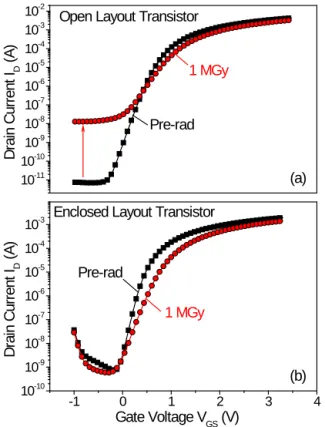
Figure 2: Drain current ID vs gate voltage VGS characteristics of two bulk
NMOS transistors: an Open Layout Transistor (OLT, top, a) and an Enclosed Layout Transistor (ELT, bottom, b) before irradiation (black squares) and after 1 MGy (red circles). Transistors are grounded during irradiation.
The open layout transistor (Figure 2a) exhibits a significant increase of the leakage current IOFF; this is due to the buildup
of oxide-trapped charge in field oxides which triggers the parasitic lateral conduction [17]. By contrast and as expected, no significant shift of the threshold voltage ΔVTH is observed,
meaning that Radiation-Induced Narrow Channel Effect (RINCE) [7,18] does not occur in the wide OLT (Figure 2a). Even so, radiation-induced effects occur at MGy dose levels despite the fact that devices are grounded during irradiation. The device response is less impacted than when devices are biased during irradiation but it remains significant. Using an enclosed geometry for transistors (ELT, Figure 2b) strongly mitigates these effects since oxide-charge trapping only occurs in the thin gate oxide. In that case, ID-VGS characteristics are
mostly changed due to the buildup of interface traps, which degrades the subthreshold slope.
Figure 3 summarizes the leakage current increase with TID measured on bulk devices. In the same time, both OLT and ELT present a decrease of the drive current ION by about 30 %
at 1 MGy. As expected, ELT presents high TID tolerance with very limited shifts of their electrical characteristics. This geometry features no interface between active silicon and thick field oxides; this intrinsically removes both the parasitic lateral conduction and RINCE.
Figure 3: IOFF shifts induced after 1 MGy on Open Layout Transistors (OLT,
black squares) and Enclosed Layout Transistors (ELT, red circles) grounded during irradiation.
The main drawback remains the significant area penalty induced by this hardening by design technique for both PMOS and NMOS transistors.
D. Partially Depleted SOI Technology
PDSOI technologies have already demonstrated their capabilities to withstand MGy dose irradiations. In the late eighties, pioneering works performed by Leray et al. [4,5,6] demonstrated the hardening potential of SOI technologies to MGy dose levels for Large Hadron Collider applications. More recently, PDSOI devices designed with external body contacts exhibited a very promising tolerance to MGy dose [8] either grounded or biased during irradiation. In such devices, the buildup of oxide-trapped charge in the BOX induces a parasitic back conduction which increases the leakage current IOFF for devices biased during irradiation. By contrast, it was
demonstrated that when devices are grounded during irradiation, the amount of trapped charge in the BOX is not enough to modify the electrical characteristics even after 3 MGy.
Figure 4: Leakage current IOFF shifts induced after 1 MGy on a Body
Contacted transistor grounded during irradiation.
10-11 10-10 10-9 10-8 10-7 10-6 10-5 10-4 10-3 10-2 (a) Open Layout Transistor
Pre-rad D rai n C ur rent ID ( A) 1 MGy -1 0 1 2 3 4 10-10 10-9 10-8 10-7 10-6 10-5 10-4 10-3 (b) Enclosed Layout Transistor
Pre-rad D rai n C ur rent ID ( A) Gate Voltage VGS (V) 1 MGy 10-3 10-2 10-1 100 0.0 1.0x10⁻⁸ 2.0x10⁻⁸ 3.0x10⁻⁸ 4.0x10⁻⁸ Enclosed Layout Leak age C ur rent ( A )
Total Ionizing Dose (MGy) Open Layout 10-1 100 101 102 5.0x10⁻¹⁰ 1.0x10⁻⁹ 1.5x10⁻⁹ 2.0x10⁻⁹ 2.5x10⁻⁹ 3.0x10⁻⁹ Leak age C ur rent ( A )
Total Ionizing Dose (MGy) Transistor with body contacts
This is confirmed by the parameter extractions plotted in Figure 4 for body contacted devices only; all electrical parameters are almost unaffected by TID. The IOFF current slightly increases when the drive current ION stays at the same
value (less than 2 % change) after a 1 MGy irradiation. Floating body transistors behave in a different manner, close to the one of bulk transistors studied in the previous section. Floating body transistors exhibit interfaces between the active silicon and field isolations contrary to body contacted devices. Such devices then suffer from the inherent parasitic lateral conduction due to buildup of oxide-trapped charge in field oxides leading to the observed IOFF increase.
E. Fully Depleted SOI Technology
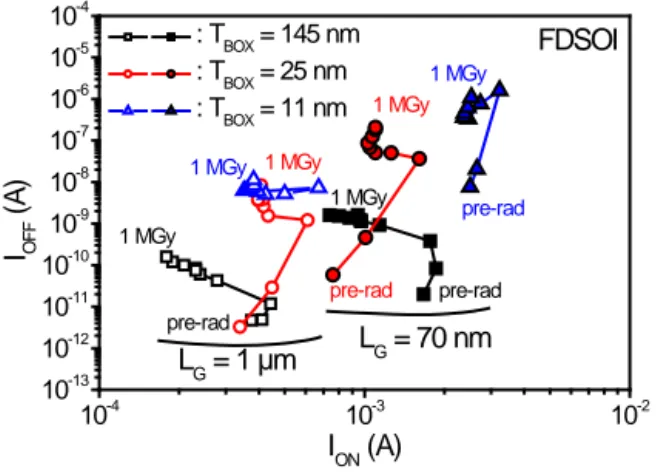
Finally, the FDSOI technology offers better scalability for nanometer scale era than both bulk and PDSOI technologies. This technology provides high performances, low power consumption and improved process variability [23,24] which are all key issues for highly integrated technologies intended for commercial market. However, its TID sensitivity is strongly governed by oxide-charge trapping in the BOX which modifies the main electrical characteristics due to electrostatic coupling effects inherent to the FDSOI structure [11]. Some papers [12,20,21,22] show that the TID sensitivity of FDSOI technologies is mainly driven by the body doping level, designed with or without body contacts, the gate length and above all the buried oxide thickness. All studies previously published were dedicated to TID below 10 kGy, so the following investigations will focus on the TID behavior of FDSOI transistors fabricated on various SOI substrates, i.e. various BOX thicknesses, at MGy dose levels. All devices were fabricated using a similar process leading to the same active silicon thickness, gate stack and doping levels. Their TID responses can thus be directly compared.
Figure 5: ION-IOFF characteristics as a function of TID on FDSOI transistors
processed on SOI substrates with a BOX thickness TBOX = 145 nm (black
squares), TBOX = 25 nm (red circles) and TBOX = 11 nm (blue triangles).
Transistors with both a short gate length (LG = 70 nm, filled symbols) and a
long gate length (LG = 1 µm, open symbols) are plotted for each SOI substrate
option. Devices are grounded during irradiation.
Figure 5 summarizes the ION-IOFF characteristics of FDSOI
devices on three different SOI substrates: TBOX = 145 nm
(black squares), TBOX = 25 nm (red circles) and TBOX = 11 nm
(blue triangles). Results for transistors with both a short gate (filled symbols) and a long gate (open symbols) are displayed.
Short gate transistors all exhibit significant modifications of their electrical performances with TID. The drive currents IOFF
increase by several decades when ION almost decrease with
TID, especially on the device with TBOX = 145 nm (filled
black squares). Decreasing the BOX thickness down to the thinnest value TBOX = 11 nm enhances the TID tolerance by
reducing the shifts reported both on ION and IOFF compared to
the other SOI substrate options. This is even more obvious on transistors with a long gate length (LG = 1 µm, open blue
triangles). Only the drive current ION exhibits variations but
with a leakage current IOFF which stays within the same order
of magnitude. Furthermore, results obtained on devices processed with Ultra-Thin BOX (UTB) substrates (TBOX = 25 nm and 11 nm) are characteristic of their overall
TID behavior since it was previously demonstrated that this behavior does not change with bias configuration during irradiation [12]. These promising results indicate that FDSOI devices may withstand high TID levels with appropriate substrate and design options, both if grounded or biased during irradiation. Obviously, standard thick BOX (TBOX = 145 nm) devices do not present such characteristic,
the NULL case being the one presenting the weakest TID induced modifications.
F. Discussion on the Hardness Potential of Modern Technologies Submitted to High TID
All investigated technologies show TID behaviors directly linked to their architecture, fabrication process, design and geometry. However, using the appropriate design options allows enhancing their TID tolerance. Figure 6 summarizes the ION-IOFF plots obtained on the most TID tolerant device for
each studied technology: bulk (black squares), PDSOI (red circles) and FDSOI (blue triangles).
Figure 6: ION-IOFF characteristics as a function of TID on FDSOI transistors for
bulk (black squares), PDSOI (red circles) and FDSOI (blue triangles) technologies. Devices are grounded during irradiation.
As a main conclusion, results presented in Figure 6 show that all devices are still functional after a 1 MGy irradiation. Their electrical characteristics change with TID but in all
10-4 10-3 10-2 10-13 10-12 10-11 10-10 10-9 10-8 10-7 10-6 10-5 10-4 1 MGy 1 MGy pre-rad 1 MGy pre-rad 1 MGy 1 MGy pre-rad 1 MGy LG = 70 nm : TBOX = 145 nm : TBOX = 25 nm : TBOX = 11 nm IOF F ( A) ION (A) L G = 1 µm FDSOI pre-rad 10-4 10-3 10-2 10-10 10-9 10-8 10-7 10-6 10-5 1 MGy pre-rad 1 MGy 1 MGy pre-rad pre-rad Bulk ELT FDSOI 1 µm FDSOI 70 nm IOF F ( A) ION (A) PDSOI with BC
cases they could be managed using the appropriate margins in the circuit design. The entire ION-IOFF characteristics must be
considered, and not only the pre- and post-irradiation results, which do not necessarily give the largest TID-induced modifications. In the case of an accident in a nuclear facility, the choice of a technology will probably be driven by the circuit function and reliability rather than by its power consumption. Indeed, one may consider that in such environment, the power consumption of a stand alone circuit will not be the first critical parameter compared to its functionality and reliability. The requirements on the drive current stability with TID would be a greater issue than the one of the leakage current.
IV. IMPACT OF ELEVATED TEMPERATURE ON MGY DOSE
SENSITIVITY
The experiments should represent the real environment as much as possible. Elevated temperatures have thus to be considered in addition to ionizing radiations for security systems in nuclear facilities. Standards for tests in such conditions recommend to anneal irradiated devices for one hour at 150 °C to qualify equipments submitted to mixed harsh environments [9,10]. Such tests have been performed on all irradiated devices presented previously but they are also completed with others performed up to 250 °C in order to discuss the annealing behavior of electronic devices in a wider range of operations.
Elevated temperatures in MOS devices usually induce recovery of radiation-induced effects [13]. Radiation-induced oxide-trap charges could be detrapped when point defects responsible for interface traps may anneal. So, elevated temperature may be an efficient way to recover electrical characteristics of pristine integrated circuits. However, using elevated temperatures is also a way to perform dynamic “life tests” which speeds up the ageing of electronic components. Irradiated devices may apparently recover electrical characteristics close to their initial ones but they could also suffer from a degraded reliability and thus a strongly lower remaining lifetime than at room temperature.
Figure 7: ID-VGS characteristics of the bulk ELT transistor after a 1 MGy
irradiation (black squares) and after the 250 °C annealing step (red circles). The transistor is grounded both during irradiation and annealing.
Figure 7 presents the typical recovery observed on irradiated MOS transistors after annealing experiments at elevated temperatures: the subthreshold slope retrieves its initial value, meaning that most interface traps are annealed after 250 °C (red circles) in this transistor. The ID-VGS
characteristics of the ELT annealed at 250 °C superimposed the characteristic measured on this transistor before irradiation (not shown for the sake of clarity) meaning that the major part of radiation-induced degradation are annealed. Such plot cannot be presented for the PDSOI transistor since no reliable parameter extractions can be done due to the weak impact of ionizing radiations induced on electrical characteristics of these transistors. Actually, no significant oxide charge and interface traps buildup occurs in the tested PDSOI devices.
FDSOI devices exhibit I-V characteristics (Figure 8) which retrieve their initial shape after annealing. This figure highlights that the curve of the device that experienced a 1 MGy irradiation followed by 250 °C annealing (blue triangles) is closely shaped like the pristine one (black squares). It means that a strong annealing of both the oxide-trap charge and the interface traps occurs in the gate oxide and the buried oxide and at each silicon-oxide interfaces respectively. These phenomena are enough to recover electrical characteristics close to the pristine one after the 150 °C annealing step (green hexagons). These results are very promising since the elevated temperature mostly counterbalances the ionizing dose effects reported in FDSOI devices even in the nominal qualification test conditions.
Figure 8: ID-VGS characteristics of a long gate FDSOI transistor before
irradiation (black squares), after 1 MGy (red circles), after 1 MGy + 150 °C (green hexagons) and after 1 MGy + 250 °C (blue triangles) The transistor is grounded both during irradiation and annealing.
Elevated temperatures strongly reduce the influence of TID on the interface traps buildup in MOS devices even at MGy dose levels. ION-IOFF characteristics retrieve values close to
their initial ones for all tested devices.
However, one should consider the entire “story” of the devices characteristics’ instead of only looking at the pre-irradiation, post-irradiation and post-annealing results. If so, most of the information on the TID and annealing behaviors would have been lost. This may lead to take circuit design
-2 -1 0 1 2 3 4 10-10 10-9 10-8 10-7 10-6 10-5 10-4 10-3 10-2
Enclosed Layout Transistor
1 MGy D rai n C ur rent ID ( A) Gate Voltage V GS (V) After 250 °C -0.5 0.0 0.5 1.0 10-12 10-11 10-10 10-9 10-8 10-7 10-6 10-5 10-4 10-3 10-2 : Before irradiation : 1 MGy : 1 MGy + 150 °C : 1 MGy + 250 °C FDSOI LG = 1 µm D rai n C ur rent ID ( A) Gate Voltage VGS (V)
margins which do not include the largest modifications induced by TID and temperature on the electrical characteristics. Finally, elevated temperatures may degrade the intrinsic reliability of electronic devices and then reduce their lifetime by several years. This should be quantified by additional dedicated tests to foresee the failure probability of security systems and their replacement periodicity.
V. CONCLUSION
This paper reviews the TID behavior of several micro- and nano-electronic devices at MGy dose levels combined with elevated temperatures. The experimental results show that design rules specific to each technology are required to ensure device functionality at MGy dose levels under elevated temperature. This paper also highlights that one has to take the entire electrical characteristics shifts’ induced by ionizing radiations and elevated temperatures to take margins enough to prevent any circuit function failure instead of taking only the pre- and post-TID/temperature test results. At first glance, elevated temperatures lower MGy ionizing dose-induced effects but their impacts on the intrinsic reliability and lifetime of electronic devices have to be quantified to properly qualify electronic systems designed for mixed harsh environments.
REFERENCES
[1] D. Fleetwood, “How To Protect Nuclear Reactor Electronics”, IEEE Spectrum Tech Talk, 2011.
[2] A.H. Johnston, “Space Radiation Effects and Reliability Considerations for Micro- and Optoelectronic Devices”, IEEE Transactions on Device and Materials Reliability, Vol. 10, n°4, p. 449, 2010.
[3] R. Lacoe, “Designing radiation hardened CMOS microelectronic components at commercial foundries: space and terrestrial environments and device and circuit techniques to mitigate radiation effects”, IEEE International Integrated Reliability Workshop Final Report, 2005. [4] J.L. Leray, “Activation energies of oxide charge recovery in SOS or SOI
structures after an ionizing pulse”, IEEE Trans. Nucl. Sci., vol. 32, n°6, pp. 3921- 3928, 1985.
[5] J.L. Leray, E. Dupont-Nivet, J.F. Pere, O. Musseau, P. Lalande, A. Umbert, “Limiting factors for SOI VLSI high-level hardness : modeling and improving”, SOS/SOI technology conference, pp. 114-115, 1989. [6] J.L. Leray, E. Dupont-Nivet, J.F. Pere, Y.M. Coïc, M. Raffaelli, A.J.
Auberton-Hervé, M. Bruel, B. Giffard, J. Margail, “CMOS / SOI hardening at 100 Mrad(SiO2)”, IEEE Trans. Nucl. Sci., vol. 37, n°6, pp. 2013-2019, 1990.
[7] F. Faccio, and G. Cervelli, “Radiation-Induced Edge Effects in Deep Submicron CMOS Transistors” IEEE Transactions on Nuclear Science, vol. 52 (6), p. 2413, 2005.
[8] M. Gaillardin, S. Girard, P. Paillet, J.L Leray, V. Goiffon, P. Magnan, C. Marcandella, M. Martinez, M. Raine, O. Duhamel, N. Richard, F. Andrieu, S. Barraud, O. Faynot, “ Investigations on the Vulnerability of Advanced CMOS Technologies to MGy Dose Environments”, IEEE Trans. Nucl. Sci., (accepted for publication), 2013.
[9] IAEA-TECDOC-118, « Assessment and management of ageing of major nuclear power plant components important to safety : in containment instrumentation and control cables », 2000.
[10] NF M64-001, « Procédure de qualification des matériels électriques installés dans l'enceinte de confinement des réacteurs à eau sous pression et soumis aux conditions accidentelles », 1991.
[11] H.K. Lim and J.G. Fossum, “Threshold Voltage of Thin Film Silicon-on-Insulator (SOI) MOSFET’s”, IEEE Trans. Electron Dev., Vol. ED-30, n°10, p. 1244, 1983.
[12] M. Gaillardin, M. Martinez, P. Paillet, F. Andrieu, S. Girard, M. Raine , C. Marcandella, O. Duhamel, N. Richard, O. Faynot, “ Impact of SOI Substrate on the Radiation Response of Ultra-Thin Transistors down to
the 20 nm Node”, IEEE Trans. Nucl. Sci., (accepted for publication), 2013.
[13] J.R. Schwank, “Total dose effects in MOS devices”, NSREC Short Course, 2002.
[14] T .R. Oldham and F.B. McLean, “Total Ionizing Dose Effects in MOS Oxides and Devices”, IEEE Trans. Nucl. Sci., Vol. 50, n°3, p. 483, 2003.
[15] T.P. Ma and P.V. Dressendorfer, Ionizing Radiation Effects in MOS Devices and Circuits, New-York: Wiley-Interscience, 1989.
[16] P.J. McWhorter, P.S. Winokur, “Simple technique for separating the effects of interface traps and trapped-oxide charge in metal-oxide-semiconductor transistors”, Appl. Phys. Lett., vol. 48, n°2, p. 133, 1986. [17] M.R. Shaneyfelt, P.E. Dodd, B.L. Draper, R.S. Flores, “Challenges in
hardening technologies using shallow trench isolations”, IEEE Trans. Nucl. Sci., vol. 45, n°6, p. 2584, 1998.
[18] M. Gaillardin, V. Goiffon, S. Girard, M. Martinez, P. Magnan, P. Paillet, “Enhanced radiation induced narrow channel effects in a commercial 0.18 µm bulk technology”, IEEE Trans. Nucl. Sci, vol. 58, n°6, p. 2807, 2011.
[19] J.R. Schwank, V. Ferlet-Cavrois, M.R. Shaneyfelt, P. Paillet, P.E. Dodd, “Radiation Effects in SOI Technologies”, IEEE Trans. Nucl. Sci., Vol. 50, n°3, p. 522, 2003.
[20] W.C. Jenkins and S.T. Liu, “Radiation Response of Fully-Depleted MOS Transistors Fabricated in SIMOX”, IEEE Trans. Nucl. Sci., Vol. 41, n°6, p. 2317, 1994
[21] J.R. Schwank, M.R. Shaneyfelt, P.E. Dodd, J.A. Burns, C.L. Keast, P.W. Wyatt, “New Insights into Fully-Depleted SOI Transistor Response After Total-Dose Irradiation”, IEEE Trans. Nucl. Sci., Vol. 47, n°3, p. 604, 2000.
[22] P. Paillet, M. Gaillardin, V. Ferlet-Cavrois, A. Torres, O. Faynot, C. Jahan, L. Tosti, S. Cristoloveanu, “Total Ionizing Dose Effects on Deca-Nanometer Fully Depleted SOI Devices”, IEEE Trans. Nucl. Sci., Vol. 52, n°6, p. 2345, 2005.
[23] C. Fenouillet-Beranger, P. Perreau, S. Denorme, L. Tosti, F. Andrieu, O. Weber, S. Barnola, C. Arvet, Y. Campidelli, S. Haendler, R. Beneyton, C. Perrot, C. de Buttet, P. Gros, L. Pharn-Nguyen, F. Leverd, P. Gouraud, F. Abbate, F. Baron, A. Torres, C. Laviron, L. Pinzelli, J. Vetier, C. Borowiak, A. Margain, D. Delprat, F. Boedt, K. Bourdelle, B.-Y. Nguyen, O. Faynot, T. Skotnicki, “Impact of a 10-nm Ultra-Thin BOX (UTBOX) and Ground Plane on FDSOI Devices for 32 nm and below”, Proc. ESSDERC, 2009.
[24] L. Brunet, X. Garros, M. Cassé, O. Weber, F. Andrieu, C. Fenouillet-Béranger, P. Perreau, F. Martin, M. Charbonnier, D. Lafond, C. Gaumer, S. Lhostis, V. Vidal, L. Brévard, L. Tosti, S. Denorme, S. Barnola, J.F. Damlencourt, V. Loup, G. Reimbold, F. Boulanger, O. Faynot, A. Bravaix, “New Insights on Vt Stability of HK/MG Stacks with Scaling in 30 nm FDSOI Technology”, Symposium on VLSI Technology Digest of Technical Papers, p. 29, 2010.