Relaxation of strained pseudomorphic Si
xGe
1−xlayers on He-implanted
Si/
␦
-Si: C / Si
„100… substrates
D. Buca,1,a兲R. A. Minamisawa,1H. Trinkaus,1B. Holländer,1N. D. Nguyen,2R. Loo,2and S. Mantl1
1
Institute of Bio- and Nanosystems, Forschungszentrum Jülich, and JARA—Fundamentals of Future Information Technology, D-52425 Jülich, Germany
2
IMEC, Kapeldreef 75, B-3001 Leuven, Belgium
共Received 6 July 2009; accepted 9 September 2009; published online 6 October 2009兲
In this letter we present a method to increase the efficiency of SiGe layer relaxation by He+ion
implantation and annealing. Preferential nucleation of He platelets along a␦-impurity layer grown in the Si substrate below the SiGe layer results in planar localization and homogenization of dislocation loop sources inducing a more uniform distribution of misfit dislocations. We demonstrate this for a thin Si:C layer grown by reduced pressure chemical vapor deposition. The optimization of the conditions for efficient relaxation and layer quality is studied with respect to the position of the Si:C layer and the process parameters. Relaxation degrees up to 85% are obtained for Si0.77Ge0.23layers. © 2009 American Institute of Physics.关doi:10.1063/1.3240409兴
Tensile strain in Si 共sSi兲 and sSi/SixGe1−x
heterostruc-tures is well known to enhance carrier mobility for high per-formance channels in complementary metal oxide semicon-ductor field effect transistors.1 A key achievement to fabricate such materials, compatible with industrial processes at wafer level, is the strain induced in Si films grown on strain-relaxed SixGe1−xvirtual substrates.2The advantageous
coupling of sSi and silicon on insulator technologies3,4 al-lows device fabrication with a better control of the electro-statics and lower power consumption.
We have previously introduced and demonstrated the usefulness of He+ion implantation and annealing to produce high quality thin 共⬃200 nm兲 relaxed SiGe layers.5,6 This concept is based on the creation of overpressurized He filled cavities of platelet shape in the ion implanted region under-neath the SiGe/Si interface during an intermediate stage of annealing. These defects eject interstitial dislocation loops that glide to the SiGe/Si interface. Here, one segment of each loop is hold at the interface as a misfit dislocation 共MD兲 segment while the other is driven by the stress through the SiGe layer to the surface forming by this two threading dis-locations 共TDs兲. The motion of the two TDs in opposite di-rections results in an extension of the MD segment leading to strain relaxation of the SiGe layer.7The generation of dislo-cation loops by overpressurized He platelets has been ob-served in Si 共Ref. 7兲 as well as in SiC 共Ref. 8兲 after He+
implantation and subsequent annealing. Note that platelet shaped He cavities tend to decay into small spherical cavities in a late evolution stage usually reached during annealing.9
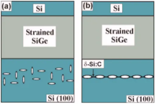
The method of relaxing SiGe layers by He implantation and subsequent annealing has limitations at low and high implantation doses. At low doses, due to low spatial density of dislocation sources, unacceptable strain fluctuations have been found in the relaxed layer. In the opposite case, at high doses, even if the high density of He cavities provides a relatively regular array of dislocation sources, their broad
depth distribution 关Fig.1共a兲兴 favors mutual dislocation loop
blocking. This limits the effective injection of mobile dislo-cation loops into the SiGe layer and, consequently, its degree of strain relaxation.
In the present work we concentrate on the mechanism of creating overpressurized He filled platelets. We present a method for preferential nucleation of He platelets in the Si substrate below the SiGe layer which results in planar
local-ization, homogenlocal-ization, and alignment of dislocation loop sources, as illustrated in Fig.1共b兲. An analytical model based on He diffusion is proposed which allows the understanding and optimization of the process conditions with respect to an enhanced relaxation of SixGe1−xlayers.
Two effects are essential: 共1兲 local enhancement of He cavity nucleation at a ␦-layer and 共2兲 suppression of cavity nucleation in its surroundings. The first effect can be realized either by reducing the energy associated with cavity forma-tion or by creating addiforma-tional volume for He accumulaforma-tion. A reduction in the cavity surface energy共determined by matrix atom binding energies兲 is obtained by locally alloying Si with Ge, e.g., by growing a SiGe or Ge␦layers.10However, this approach has the disadvantage that the effective lattice volume required for the accumulation of He interstitial atoms is reduced. A more genuine approach is the use of a Si:C layer embedded in the Si substrate. Recently, the effects of
interstitial C on the helium-induced cavities in carbon
im-a兲Electronic mail: [email protected].
FIG. 1. 共Color online兲 Schematic of the He cavity distribution forming in the Si substrate without 共a兲 and with 共b兲 an epitaxial ␦-Si: C layer. The presence of the␦-Si: C layer changes the broad depth distribution of the He platelets共a兲 to a localized, uniform, and aligned one 共b兲.
APPLIED PHYSICS LETTERS 95, 144103共2009兲
0003-6951/2009/95共14兲/144103/3/$25.00 95, 144103-1 © 2009 American Institute of Physics
planted silicon during high-temperature annealing have been described.11D’Angelo et al.10have discussed the role of
sub-stitutional C on cavity formation at high irradiation
condi-tions. The authors interpret the enhancement of cavity nucle-ation in relatively thick layers共20 nm兲 as a consequence of the strain induced by the C incorporation in the Si lattice.12 However, applications require a detailed experimental and theoretical analysis of the effect of enhanced cavity nucle-ation along embedded SiGe共Ge兲 or Si:C layers on the relax-ation process of SiGe layers, not available up to date.
Here, we report on the use of a buried ultrathin Si:C layer共␦-Si: C兲 on the Si共100兲 substrate to improve the relax-ation of epitaxial strained SixGe1−xstructures. Our goals are
to optimize the process parameters with respect to the strain relaxation of SiGe layers and the quality of the heterostruc-tures, and to propose a mechanism of localized He cavity formation in the buried␦-Si: C layer.
180 nm thick strained Si0.77Ge0.23layers were grown on
200 mm p-type wafers of pure Si共001兲 and on wafers con-taining a single epitaxially grown␦-Si: C共then buried兲 layer. The ␦-Si: C layer had a targeted substitutional carbon con-centration of about 1 at. % and a layer thickness of 2 nm. Pure Si spacers of thicknesses hSiC= 100, 150, and 200 nm
were deposited before the growth of the Si0.77Ge0.23layer. All
structures were grown by chemical vapor deposition in an ASM Epsilon®production tool. The SiGe layers were capped with 6 nm Si layers which become tensely strained by plastic strain transfer during the relaxation of the SiGe layers as demonstrated in Ref.5. A tensile stress of about 1 GPa was obtained in the top Si layer for a degree of relaxation of 70% of the SiGe layer. The heterostructures were implanted at room temperature with He+ ions to doses between
7⫻1015 cm−2 and 2⫻1016 cm−2 using energies such that the projected range Rp is located above, below and at the
␦-Si: C layer position. For easier data presentation, we use the mean ion distribution depth hpcounted from the SiGe/Si
interface, hp= Rp−共hSiGe+ hSi兲, where hSiGe and hSi are the
SiGe and Si cap layer thicknesses, respectively. After im-plantation, samples were annealed in a rapid thermal anneal-ing system at a temperature of 850 ° C for 600 s in inert atmosphere. Reference wafers without the additional␦-Si: C layer were processed at the same conditions. The degree of relaxation of the SiGe layers 共RSiGe兲 was measured by
Ra-man spectroscopy using a 415 nm wavelength and low laser power density.
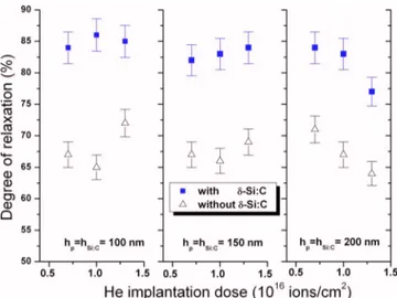
The relaxation degrees of the Si0.77Ge0.23layers with and
without the ␦-Si: C layers grown at hSiC= 100, 150, and
200 nm below the SiGe interface, are shown in Fig. 2 as a function of the He-implantation dose, for the case of
hSiC= hp. For all the implanted samples, the ␦-Si: C layer
induces an average increase of about 20% of the SiGe relax-ation degree with respect to the reference wafers. We at-tribute this relaxation increase to an enhanced cavity nucle-ation in the ␦-Si: C layer due to an increase in the volume available for He atoms on the six octahedral interstitial sites nearest to each substitutional C atom 共note that, with an atomic volume of 5.68 Å3, C atoms are small compared to Si matrix atoms having an atomic volume of 20 Å3兲.
It is useful here to discuss the proper choice of the in-trinsic parameters of the␦-Si: C layer, the C concentration, x, and the layer thickness dSi:C, assuming that, for the low
im-plantation doses used in the present experiments, the major
part of substitutional C atoms is conserved in the layer after the He+ ion implantation. Localization of cavity nucleation
may be considered to become optimal when, before nucle-ation occurs, a diffusing He interstitial atom penetrating the layer from outside has a significant probability for getting trapped close to a C atom even in the middle of the ␦-Si: C layer. This qualitative condition may be quantified by requir-ing that the mean He diffusion length in the␦-layer is about half of the layer thickness ldiff⬇dSi:C/2. In a continuum
dif-fusion approach, the mean difdif-fusion length in a medium con-taining sinks is given by ldiff= 1/k where k2is the strength of
the sinks.13Approximating the octahedron formed by the 8 interstitial sites around each C atom by a spherical sink of trapping radius rtr= a/2 where a is the lattice constant, and
using k2= 4r
trNtr, where Ntr= NC= 8x/a3is the number
den-sity of traps 共C atoms兲, we may write
D = dSiC/2ldiff⬇ 2
冑
xdSiC/a ⬇ 1. 共1兲For D⬍1, the Si:C layer is not efficient for He cavity local-ization while for D⬎1, separate cavity layers must be ex-pected to form at each side of the Si:C layer. The latter situation is confirmed by the cross-section transmission elec-tron microscopy 共XTEM兲 image of a sample with a␦-Si: C layer 200 nm below the SiGe/Si共100兲 interface, presented in Fig.3. In the figure inset, locally double cavity layers formed at the ␦-Si: C layer position are exemplified. This result in-dicates that our samples do not fully satisfy the condition for ideal localization of cavity nucleation defined by Eq. 共1兲
FIG. 2. 共Color online兲 Comparison of relaxation degrees of 180 nm Si0.77Ge0.23layers obtained by He implantation and annealing in the
pres-ence 共squares兲 and absence 共triangles兲 of Si:C layers for different layer positions hSiCand implantation depth hp= hSiC共optimum case兲 as a function
of He+implantation dose.
FIG. 3. XTEM image of a 180 nm Si0.77Ge0.23layer relaxed by a 40 keV
implantation of 1.3⫻1016 He+ions/cm2. The inset shows a magnification
of a double cavity layer formed adjacent to the␦-Si: C layer.
144103-2 Buca et al. Appl. Phys. Lett. 95, 144103共2009兲
which would also fit to the value of
D⬇1.85⬎1 obtained using in Eq. 共1兲 dSi:C= 2 nm and the
targeted value for x.
Trapping of diffusing He interstitial atoms in the␦-Si: C layer is associated with a reduction of the He concentration in regions adjacent to the layer. This results in a reduction of cavity nucleation and dissolution of initially formed cavity embryos in the surroundings of the layer which manifests itself in depleted zones共DZs兲 at both sides of the layer.8The temporal evolution of the width w of these zones depends on the implanted He concentration, cHeimpl, and the annealing temperature T as8 wdw/dt ⬃ DHe共T兲cHe int共T兲/c He imp , 共2兲
where DHe共T兲 is the diffusivity and cHeint共T兲 is the
concen-tration of interstitial He in Si共He in solution兲. According to Eq. 共2兲, the final width of the DZ can be controlled, via
cHeint共T兲, by the He-implantation dose and, via DHe共T兲 and cHeint共T兲, by the annealing temperature. In the ideal case, the
total width of the two DZs at both sides of the␦-Si: C layer 共plus the ␦-Si: C layer width兲 equals the He distribution profile.
Results for the relaxation degree of SiGe layers obtained for He implantation at depths different from the positions of the ␦-Si: C layers共hSiC⫽hp兲 are presented in Fig.4共a兲. For hSiC⬎hp, where most of the He distribution profile is
posi-tioned between the SiGe/Si interface and ␦-Si: C layer, the relaxation degree of the SiGe layers is only somewhat lower but less sensitive to the increase in implantation dose than under optimal conditions. In the present case, the interface also acts as a He-getting site in addition to the␦-Si: C layer. We have previously reported14 that, despite of a high relax-ation degree of the SiGe layer, cavities at the interface act as obstacles against the propagation of TDs, thus leading to a dose independence of the relaxation process but also to a strong decrease of the crystalline quality of the relaxed SiGe layer.
For hp⬎hSiC, the effect of the ␦-Si: C layer becomes
significant if the implanted He volume density is sufficiently large at the ␦-Si: C layer position. Calculations using the
SRIM simulation code15 for the doses applied in this work
yield for hSiC= 100 nm and hp= 200 nm densities of
1 to 2⫻1020 He/cm3at the␦-Si: C layer position, which are
known to be sufficient for He cavity nucleation at interfaces.14,16 For hSiC= 100 nm and deeper implantation
hp= 300 nm, only the high dose implantation of
2⫻1016 cm−2 fulfills this condition; the low doses result in He densities below 3⫻1019 cm−3. These estimates explain
the lower degree of relaxation of the SiGe layer for the case of lower dose and deep implantation, as shown in Fig.4共b兲. In addition, for a deeper␦-Si: C layer position, the reduction of the elastic image force pulling the dislocation loops formed at the ␦-Si: C layer toward the sample surface de-creases the SiGe relaxation degree to similar values obtained in the absence of the␦-Si: C layer.
In summary, we have shown that the relaxation degree of SiGe layers can be increased by introducing a buried␦-Si: C layer in the Si共100兲 substrates. This enhancement is attrib-uted to localization, homogenization, and alignment of the He cavities along the layer plane improving the dislocation dynamics responsible for strain relaxation. The preferential nucleation of He cavities along a␦-Si: C layer is modeled in terms of the diffusion of He interstitial atoms to the layer and their trapping and agglomeration there. Under optimal im-plantation conditions, a buried ␦-Si: C layer leads to an in-crease in the relaxation degree of a He-implanted 180 nm Si0.77Ge0.23 layer by about 20%, inducing an elastic stress
transfer to the top Si epilayer ofsi= 1.35 GPa.
This work was partially supported by the German Fed-eral Ministry of Education and Research within the frame-work of the MEDEA⫹DECISIF project共2T 104兲.
1Y. J. Mii, H. Y. Xie, E. A. Fitzgerald, D. Monroe, F. A. Thiel, B. E. Weir,
and L. C. Feldman,Appl. Phys. Lett. 59, 1611共1991兲.
2E. Fitzgerald, Y.-H. Xie, M. Green, D. Brasen, A. Kortan, J. Michel, Y.-J.
Mii, and B. Weir,Appl. Phys. Lett. 59, 811共1991兲.
3C. Mazure and A.-J. Auberton-Hervé, Proceedings of the 31st European
Solid-State Circuits Conference (ESSCIRC 2005), Grenoble, France 共IEEE, Piscataway, NJ, 2005兲, p. 29.
4M. Reiche, C. Himcinschi, U. Gösele, S. Christiansen, S. Mantl, D. Buca,
Q. T. Zhao, S. Feste, R. Loo, D. Nguyen, W. Buchholtz, A. Wei, M. Horstmann, D. Feijoo, and P. Storck,ECS Trans. 6, 339共2007兲.
5D. Buca, S. F. Feste, B. Holländer, S. Mantl, R. Loo, M. Caymax, R.
Carius, and H. Schaefer,Solid-State Electron. 50, 32共2006兲.
6D. Buca, B. Holländer, S. Feste, St. Lenk, H. Trinkaus, S. Mantl, R. Loo,
and M. Caymax,Appl. Phys. Lett. 90, 032108共2007兲.
7H. Trinkaus, B. Holländer, S. Rongen, S. Mantl, H.-J. Herzog, J.
Kuchenbecker, and T. Hackbarth,Appl. Phys. Lett. 76, 3552共2000兲.
8J. Chen, P. Jung, and H. Trinkaus,Phys. Rev. B 61, 12923共2000兲. 9N. Hueging, M. Luysberg, H. Trinkaus, K. Tillmann, and K. Urban,
J. Mater. Sci. 41, 4454共2006兲.
10D. D’Angelo, S. Mirabella, E. Bruno, A. Terrasi, C. Bongiorno, F.
Giannazzo, V. Raineri, G. Bisognin, and M. Berti,J. Appl. Phys. 103,
016104共2008兲.
11V. M. Vishnyakov, S. E. Donnelly, and G. Carter,J. Appl. Phys. 94, 238
共2003兲.
12D. D’Angelo, S. Mirabella, E. Bruno, G. Pulvirenti, A. Terrasi, G.
Bisognin, M. Berti, C. Bongiorno, and V. Raineri,J. Appl. Phys. 104,
023501共2008兲.
13A. D. Brailsford and R. Bullough,Philos. Trans. R. Soc. London, Ser. A
302, 87共1981兲.
14D. Buca, M. J. Mörschbächer, B. Holländer, M. Luysberg, R. Loo, M.
Caymax, and S. Mantl, Mater. Res. Soc. Symp. Proc. 809, 15共2004兲.
15J. F. Ziegler, J. P. Biersack, and U. Littmark, The Stopping Range of Ions
in Solids (SRIM—The Stopping and Range of Ions in Matter)共Pergamon, New York, 1985兲,http://www.srim.org/.
16V. Raineri, P. Fallica, G. Percolla, A. Battaglia, M. Barbagallo, and S.
Campisano,J. Appl. Phys. 78, 3727共1995兲.
FIG. 4.共Color online兲 Relaxation degree of Si0.77Ge0.23layers as a function
of implantation dose for the nonoptimum conditions: hSiC⫽hp: 共a兲
hSiC⬎hp and 共b兲 hSiC⬍hp. Full and empty symbols correspond to hSiC
= 100 and 200 nm for various hpdepths, respectively.
144103-3 Buca et al. Appl. Phys. Lett. 95, 144103共2009兲