Science Arts & Métiers (SAM)
is an open access repository that collects the work of Arts et Métiers Institute of
Technology researchers and makes it freely available over the web where possible.
This is an author-deposited version published in:
https://sam.ensam.eu
Handle ID: .
http://hdl.handle.net/10985/16608
To cite this version :
Aurélien BESNARD, Maria-Rosa ARDIGO, Luc IMHOFF, Philippe JACQUET - Curvature radius
measurement by optical profiler and determination of the residual stress in thin films - Applied
Surface Science - Vol. 487, p.356-361 - 2019
Any correspondence concerning this service should be sent to the repository
Administrator :
archiveouverte@ensam.eu
Curvature radius measurement by optical profiler and determination of the
residual stress in thin films
A. Besnard
a,⁎, M.R. Ardigo
a,b, L. Imhoff
b, P. Jacquet
a,caArts et Metiers ParisTech, LaBoMaP, Rue Porte de Paris, 71250 Cluny, France
bLaboratoire Interdisciplinaire Carnot de Bourgogne (ICB), UMR 6303 CNRS - Université de Bourgogne, BP 47870, 21078 Dijon Cedex, France cPôle Matériaux et structures, ECAM Lyon, 40 Montée Saint Barthélemy, Université de Lyon, 69321 Lyon Cedex, France
A B S T R A C T
The Stoney formula, based on the measurement of the substrate curvature, is often used for the determination of the thin films' residual stress. In this study, titanium nitride coatings were deposited by DC reactive magnetron sputtering on silicon substrates. An optical profiler was used to determine the curvature of the surface before and after coating. Two radii were then obtained, along the principal perpendicular directions of the surface curva-ture. A simple and efficient method to determine the experimental error on the stress calculation was developed taking into account the film thickness dispersion and the radii dispersion. Using constant deposition parameters, some samples' characteristics were tested: film and substrate thickness, size, shape and crystallographic or-ientations of the substrates. With the help of the developed error method, we analyzed what can be conclude about the influence of these characteristics on the calculated stress values, obtained from the experimental measurements.
1. Introduction
Stress determination in thin films is a common thematic in litera-ture, as it has an impact (in a positive or a negative way) on several scientific and practical applications [1,2]: mechanical and protective coatings, sensors, optical devices, or films with a specific physical/ chemical function (thermal, magnetic, electrical, biological…). There are three main approaches in the study of stress in thin films. The major and uncountable part of publications mentions stress only as one among other film properties. Some authors use the XRD technique [3–5], other the curvature method [6,7], few both techniques [8]. In these studies, the calculated stress values are put in relation to film properties (i.e. hardness, grain size, thickness, composition, etc.) or to process para-meters (power, temperature, pressure, etc.). Other authors work on the in-situ measurements of the stress to understand the initial stages and the origin of stress [1,9–11]. Finally, the last group of research concerns the theoretical study of the stress-strain relation with analytical models and FEM computations. In this domain, the reference publication is the one of G. G. Stoney [12] and, more recently, a review was published by Janssen [13]. In these works, the limits of the Stoney formula are stu-died in detail based on mechanical and theoretical considerations. However, very little information can be found in the literature about the limits of this method from a measurements point of view. In other
words, plenty of models, behaviors, theories, corrections, all as much interesting and valuable as the other, can be found, but nearly nothing about determining a stress value which has a sense and can be used in this kind of analyses. Consequently, the aim and novelty of this paper is to fulfil this lack and to give some practical clues about the estimation of the relevancy of the calculated stress values. Regarding the appli-cations, the added value consists in the possibility to make choices based on simple and reliable analyses. If the results can be trusted, it allows then to build models and to correlate then with other set of data, or to define optimum deposition condition customized for a specific application. If the error bars are too large, researches must be reor-iented to eventually obtain better results. The main gain is on the time spent working on erroneous models, which could conduct to dramatic and unjustified choices. This study will be done with different substrate and film configurations, but always in the theoretical validity range of the Stoney formula and under a constant deposition process (except time), i.e. with a unique origin of stress.
The Stoney formula is detailed in Eq.(1):
= E 6(1 ) h h 1 R 1 R s s s 2 f 0 (1)
where Esis the Young's modulus and νsthe Poisson's ratio of the sub-strate; hsand hfare, respectively, the substrate and the film thicknesses; ⁎
Corresponding author.
E-mail address:aurelien.besnard@ensam.eu(A. Besnard).
R0and R are respectively the curvature radii of the substrate before and after the deposition process.
Analyzing Eq.(1), it is clear that the main critical point here is the measurement of the curvatures R0 and R and, consequently, the de-formed shape related to the strain. Indeed, substrate properties are well known and the film thickness can be determined with a high precision by scanning electron microscopy. In this work, a particular attention will be given to the measured radii and the stress will be calculated in relation to different film (thickness) and substrate (thickness and crystallographic orientation) properties for constant process para-meters. The TiN film, a classical and well known hard coating, was chosen only as example to illustrate the analyses presented in the study. The thermal stress, given by Eq.(2)[14], is supposed to be negli-gible in our conditions:
= E ( )(T T )
th f f s S M (2)
with Ef the Young modulus of the film, αfand αs the film and the substrate thermal expansion coefficients, TSthe substrate temperature during deposition, TMthe temperature at which the thermal stress is determined, or at which the coating system operates in service. Nevertheless, a discussion about a possible thermal effect during de-position will be presented inSection 3.4.
2. Material and methods
TiN coatings were deposited by DC reactive magnetron sputtering on silicon substrates using a rectangular (12 × 40 cm x cm) titanium metallic target (purity 99.99%) in an Ar + N2gas mixture (40 and 90 sccm respectively). The discharge voltage was about −380 V with a current density of 29 mA.cm−1. The working pressure was 0.65 Pa and the fixed target-to-substrate distance was 9.5 cm. In these conditions the growth rate of the TiN film was about 83 nm.min−1. The deposition time was adjusted to obtain different TiN film thicknesses from 250 to 3400 nm. Before the deposition process, the silicon substrates are cut from a one (380 μm) or two (280 μm) side mirror-polished wafer, cleaned with ethanol in an ultrasonic bath, dried and kept at room temperature. All samples are extracted from the same wafer, with re-spect of the thickness and crystallographic orientation.
Table 1 summarizes the combination between the different sub-strate characteristics and the film thicknesses.
The surfaces and the cross-sections of the samples were analyzed using a JEOL JSM-7600F scanning electron microscope (SEM) equipped with a field emission gun (FEG). The film structure was determined by X-ray diffraction (XRD) using Co Kα (λ = 1.789 Å) radiation at fixed low incidence angle (5°).
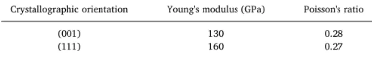
For the calculation of the residual stress, the values used for the Young's modulus (Es) and the Poisson's ratio (νs) of the substrate, which depend on its crystallographic direction, are listed inTable 2[15–17]. The thickness of the substrates (hs) was given by the suppliers and the thickness of each film (hf) was measured by SEM. The surface curvature γ was measured by an optical profiler (WYKO NT1100) be-fore and after TiN deposition, considering the whole surface of the sample. The curvature analysis was made by Gwyddion software [18],
which allows determining the principal curvatures of the surface along the orthogonal directions. The principal curvatures in an Euclidian space correspond to the minimum and the maximum of the curvatures of a surface and are sufficient to describe a surface.
After surface measurements, two analyses are available:
•
determining separately the initial and final surfaces characteristics: principal directions (φ0.1, φ0.2and φ1, φ2) and corresponding radii before and after coating (R0.1, R0.2and R1, R2respectively) and subtracting the inverse of the radii in the Stoney formula;•
subtracting the initial and final surfaces images and determining the characteristics of the equivalent surface corresponding to the de-formed shape from a pure flat state (φeq1, φeq2and Req1, Req2). The second way is more relevant for the stress calculation and minimizes the measurement errors, due to the lower number of op-erations. Indeed, in the first way, the principal directions of curvature are in most of the case different before and after coating. There is here the question of the relevancy of subtracting two values (here the cur-vature) which are not applied at the same point nor within the same direction. It is possible that the error remains low, especially if the substrate presents a near-spherical curvature, but from a mechanical point of view it has no sense.From the equivalent surface, two radii are extracted. If the fifth hypothesis of the Stoney theory is respected (i.e. spherical deformation) [19], Req1, Req2 are equal; this is mostly not the case, whatever the reason. Because the aim of this work is to obtain a global stress cal-culation and because the Stoney formula needs only one radius value, a choice has to be done by the user. Either the maximum radius, which will lead to the minimum stress, or the minimum radius, which will lead to the maximum stress, or, as last choice, the radius corresponding to the average curvature (Eq.(3)):
= + R R R R R 2 eq eq eq eq 1 2 1 2 (3)
The average radius =R Req1+2Req2is only a mathematical value that has no physical sense for the description of the surface curvature. In most of the cases, the error remains small (e.g. for a relative radius errorRR = 100%
min , the relative function error
R R
R is about 12.5%),
but in order to minimize the stress error, only R should be used. The dispersion of the calculated stress values is determined with both experimental dispersion of the film thickness and radii using Eqs.
(4) and (5). = E h h R 6(1 ) 1 min s s s fmax eq max 2 (4) = E h h R 6(1 ) 1 max s s s fmin eq min 2 (5) The stress is therefore flanked by two minimal and maximal values, reflecting the precision of both thicknesses and radii measurements. This novel and simple method, directly derived from the experimental, gives a good indication of the relevancy of the calculated stress value. With this experimental error, the possible stress evolution with a given parameter can be investigated correctly.
Table 1
Samples parameters.
Substrate Film
Shape Size (mm × mm) Thickness and orientation Thickness (nm)
Square 10 × 10 380 μm (001) 475, 1050, 2200 15 × 15 Rectangle 10 × 13 10 × 15 10 × 20 280 μm (001) 250, 430, 3400 280 μm (111) Table 2
Silicon Young's modulus (Es) and Poisson's ratio (νs) for two crystallographic
orientations.
Crystallographic orientation Young's modulus (GPa) Poisson's ratio
(001) 130 0.28
3. Results and discussion
3.1. Structural characterizations of the coated samples
XRD analyses of the surfaces of the coated samples confirmed the formation of TiN with a (111) preferred orientation. A secondary and minor (202) orientation was also detected. For the thicker TiN film (3400 nm) the preferred orientation is still (111), but with traces of (311), independently of the thickness and the crystallographic or-ientation of the substrate.
SEM cross-section and surface morphologies of the 2200 (a), 1050 (b) and 475 (c) nm TiN coatings on 380 μm (001) Si substrate are shown inFig. 1.
Cross-section observations show a columnar-type structure. For all thicknesses the coating is rather compact and homogeneous. The col-umns' head can be observed on SEM top view images (Fig. 1Insets). In agreement with Abadias et al. [8], they are formed by pyramid-shaped (111) grains, whose size increases proportionally to the coating thick-ness. Following Chason et al. [9], it means that the stress should de-crease with the inde-crease of the film thickness. This behavior is obviously not due to the film thickness, but to the growth mechanisms drove by the deposition conditions and the quantity of energy available per im-pinging atom.
3.2. Influence of the sample's shape and size
Fig. 2shows the calculated residual stress versus the radiusR va-lues for the 2200, 1050 and 475 nm films deposited on 380 μm (001) silicon substrates of different shapes and sizes.
The black lines correspond to the Stoney equation function of the radius for a given film thickness. Triangle marks with the tip up
correspond to the maximum stress value calculated from the overall Reqmin, while triangle marks with the tip down is the minimum value calculated from the overall Reqmax. Error bars represents here the in-fluence of the thickness variation applied to Stoney formula with R . Due to the curve progression of the Stoney equation the values of the error bars increase with a decreasing radius. The stress domain defined by σminand σmaxis rather constant and comprised between 75 MPa and
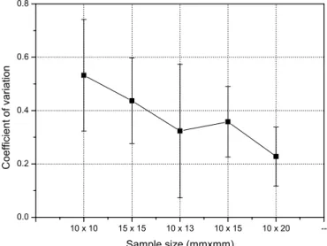
225 MPa and thus whatever the thickness of the films. In contrary, considering only the stress calculated from R , the results show a in-fluence of the film thickness: the thicker the film is, the lowest the dispersion of the calculated stress for the different samples is. For a thickness of 2200 nm, the average stress is about 137 MPa with a standard deviation of 4 MPa, for a thickness of 1050 nm, the average stress is about 131 MPa with a standard deviation of 18 MPa and for a thickness of 475 nm the average stress is about 158 MPa with a standard deviation of 25 MPa. If the stress seems to increase with the decrease of the film thickness, this conclusion is weakened by the increase of the dispersion. Considering the size and shape of the samples, no general trends could be reported for the stress evolution in comparison to the film thickness evolution: decrease for the 10 × 10, increase for 15 × 15 and 10 × 20, decrease and then increase for 10 × 13 and 10 × 15. To conclude on this influence, the dispersion in the radii measured for all sample is examined. Hence,Fig. 3represents the coefficient of variation between Req1and Req2,averages for the three coating thicknesses.
A shape effect can be clearly observed: when the shape of the sample approaches to a strip (corresponding to the 10 × 20 mm x mm sample in our case) the deformation after coating tends to become more spherical, satisfying Stoney's hypothesis. This behaviour is in agreement
Fig. 1. Cross section and surface morphologies of the TiN films on (001) silicon substrates: (a) 2200, (b) 1050 and (c) 475 nm coating thicknesses.
0 20 40 60 80 100 120 0.05 0.10 0.15 0.20 0.25 e = 475 nm e = 1050 nm 10 x 10 15 x 15 10 x 13 10 x 15 10 x 20 Max Min S tr e ss (G Pa ) Radius (m) e = 2200 nm
Fig. 2. Calculated residual stress versus the radius R for 2200, 1050 and 475 nm film thicknesses deposited on 380 μm (001) Si substrates of different shapes and sizes.
10 x 10 15 x 15 10 x 13 10 x 15 10 x 20 --0.0 0.2 0.4 0.6 0.8 C o e ff ici e n t o f va ri a ti o n Sample size (mmxmm)
Fig. 3. Radii coefficient of variation for the 2200, 1050 and 475 nm film thicknesses deposited on 380 μm (001) Si substrates with different size and shape.
with the FEM results of Guyot et al. [20]. These results were presented in a different way in a previous study [21], and the experiments were reproduced by Shiri et al. [22] in the case of DLC films, adding round-shape substrates. In opposition to the present results, they found for all substrate shapes a constant stress value of 760 MPa ± 100 MPa, about 5 times higher than in our study. Higher stress implies more deforma-tion and consequently a smaller radius and a higher sagitta. Whatever the substrate size, the curvature measurement can be performed with a sufficient accuracy. Moreover, due to the hyperbolic shape of the Stoney equation (Fig. 2), for high stress level the possible radius range is shorter, i.e. the deformation becomes spherical. It means that, whatever the substrate shape, its influence will be small. In summary, more the film is stressed, more the substrates shape and size can be neglected. If the stress level is previously known (and sufficiently high), any substrate shape could be used. In a prospective study, the user should prefer the greater strip-like substrate as possible. In general, small substrates with arbitrary shapes (e.g. sample extracted from the wafer sides) must be avoided. Finally, it is also obvious, with the dis-persion reported here, that the substrate dimensions are given at the half millimeter, or the millimeter. What is important is working with a large enough internal surface and not specific and precise external di-mensions.
3.3. Influence of the coating thickness
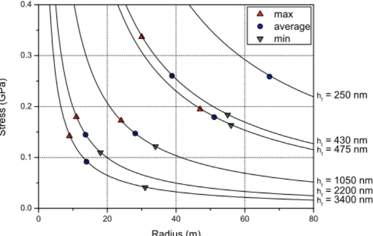
Taking into account the previously presented results, we chose to work only with 10 × 20 mm2samples, for the further analyses. In a first time, we focused on the 380 μm (001) Si substrate, one side mirror-polished. Several TiN thicknesses were considered: the first set with 2200, 1050 and 475 nm and an additional set with 3400, 430 and 250 nm.Fig. 4shows the calculated residual stress versus the radiusR for the different coating thicknesses.
As previously observed for different sample geometries and in agreements with the grain size evolution (Fig. 1), the stress tends to increase when the film thickness decreases. Moreover, the error con-cerning the residual stress values calculated becomes more important for the thinnest coatings. The dispersion values concerning the 250 nm TiN thickness are not reported on the graph. Indeed, for this thickness, a near saddle-like surface is observed (R1= 30 m and R2= −280 m) and leads to a variation in stress of ± 0.321 GPa. It implies at the same time high tensile stress (0.724 GPa) and low compression stress (−0.078 GPa) in the film. But, it as to be noted that the R2value is really high, and consequently not really relevant from an experimental point of view, due to the high measurement uncertainty, and in parti-cular the sign of the radius.
It can be concluded that not only the shape of the sample, but also
the film thickness is a critical parameter for the stress calculation, and this, without any consideration about the real stress state. They both have to be taken into account carefully when the Stoney formula is used, to ensure the relevance of the studies.
Even if a stress value can be calculated (and it is always possible to enter data in the Stoney formula) the results can be meaningless. Following the theoretical stress curves (Fig. 4), it is possible to de-termine two experimental problematic cases (values are given as order of magnitude, not as precise points):
•
low thicknesses (< 250 nm) and high radii (> 100 m),•
high thicknesses (> 2 μm) and small radii (< 5 m).In this both cases, the relative errors (in thickness and radii) can be important, leading to a high relative stress error. Because, for a given film synthesized during a given process, the stress (and consequently the value of the measured radius) could not be predicted, the only way to control the relevancy of the stress calculation is the use of Eqs.(4) and (5).
Without this precaution, and depending of the choice (user depen-dent) of the radius value (minimal, maximum, average radius or radius of the average curvature), all behaviors could be found for the influence of thickness on the stress: from no influence with a constant stress value around 150 MPa to strong influence with an increase of the stress from 50 MPa to > 500 MPa with the decrease of the thickness and any other intermediate behavior. This problem is present for this kind of global analyses, where the stress is calculated ex-situ, but not for in-situ measurements, where the evolution of the deformation is measured. As a consequence, in ex-situ measurements, any stress evolution must be completed by several other parameters to reach a trend of behaviors and conclude.
3.4. Influence of the temperature during the process
The previous results, according to a common analysis in the litera-ture, tend to show an increase of the stress with the decrease of the film thickness. But because thickness is, like the stress, a consequence of the film growth in relation with the deposition parameters, an examination of the substrate temperature was conducted during dedicated deposi-tion, keeping constant other process parameters: pressure, voltage, current density and consequently deposition speed. For the 3 thinnest films, a strong temperature increase is noted from ambient to 200 °C, corresponding to the transient mode of the heat transfer in the sputter system (energetic particles and radiation from the plasma as heat source, cooling system of the chamber as limit conditions and the substrate holder as exchange system). For longer deposition times, the system enters in the steady-state mode with a progressive stabilization of the temperature near 300 °C. Shaginyan et al. [23] report similar substrate temperature evolution and introduce the Hot Thin Surface Layer, which can be more relevant in term of microstructural evolution (and their consequence on the stress) than the thermal stress.
Compared to the substrate temperature, the stress presents an ob-vious linear decrease with a chi-square of 0.9. This result seems to imply that the thermal conditions are responsible of the stress in the films at different levels. Firstly, the increase of the substrate tempera-ture will increase the adatoms mobility and thus reinforce the increase of the grain size with the increase of the film thickness. Secondly, the duration at high temperature (deposition time and natural cooling down before the chamber opening) could have act as an annealing with stress relieving. Thirdly, the thermal stress should probably not be ne-glected as supposed in the introduction. But, the main limit to de-termine the thermal stress is the need of the film properties: Young modulus and thermal expansion coefficient. Without experimental measurements of these properties of the films, data of the literature could be used, even if the large dispersion of these values doesn't really allow this calculation. As an example,Table 3 presents the range of
0 20 40 60 80 0.0 0.1 0.2 0.3 0.4 hf= 475 nm hf= 430 nm h f= 1050 nm h f= 2200 nm h f= 3400 nm St re ss (G Pa ) Radius (m) max average min h f= 250 nm
Fig. 4. Calculated residual stress for different film thicknesses deposited on 10 × 20 mm2380 μm (001) Si substrates.
possible thermal stress with the extreme values given by the literature. The substrate thermal expansion coefficient used in the calculation is 3.6 10−6K−1[14]. The limit temperatures used in the calculations are 67 and 290 °C.
It is nearly impossible to conclude from the data reported inTable 3. Indeed, following Vaz [8] for the thermal expansion coefficient, the thermal stress is compressive, where with Pierson [24] it is tensile. In the first case, the intrinsic stress tends to decrease less with the tem-perature, tending to a constant intrinsic stress state. In the second case, the intrinsic stress is tensile for small thicknesses and becomes com-pressive for higher thicknesses. The choice of the Young Modulus only changes the magnitude of the calculated thermal stress. However, one should note that the values given by Pierson are those of the bulk TiN and thin films properties are commonly known to present lower values. For this reason, the values given by Vaz, with a film thermal expansion coefficient of 2.9 10−6K−1 and a Young modulus between 100 and 200 GPa are chosen in the present study. Nevertheless, taking into ac-count this thermal stress in the previous calculations, even with the highest Young modulus values, only lowers the slope of the graph (Fig. 5) and doesn't change the previous conclusions. The resulting in-crease in the intrinsic stress remains, in all cases, smaller than the error bars.
3.5. Influence of the substrate thickness and orientation
Because a silicon wafer doesn't present isotropic characteristics, the crystallographic orientation should have an influence on the strain and consequently on the calculated stress [11]. In the previous parts of this paper, we used classical (100) silicon substrate; in this part we added the (111) orientation, more isotropic. The supplementary changes, i.e.
substrate thickness and number of polished sides, are due to the supplier. The surface finishing of the back side of the wafer should nothave an influence. Or if it has, a serious reassessment of all the litera-ture using the curvalitera-ture measurements must be done. The substrate thickness is not a problem because it is taken into account in the for-mula.
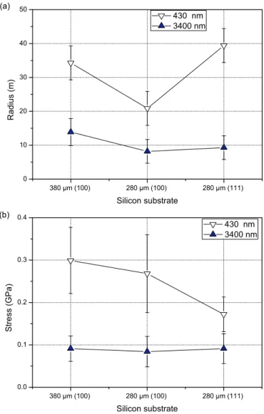
Fig. 6shows the evolution of theR values (a) and the residual stress calculated (b) in function of the thickness and the crystallographic or-ientation of Si substrates having the same shape and size (10 × 20 mm2) for two film thicknesses.
For a thick coating (3400 nm), a decreasing of the substrate thick-ness is accompanied by a diminishing of theR value; no influence of the crystallographic orientation of the substrate can be observed (Fig. 6(a)), in the case of equivalent substrates. When the residual stress is considered (Fig. 6(b)), no significant differences between the three silicon substrates can be observed. This proves the relevancy of the Stoney formula: a given deposition process produces films with a con-stant stress level. For a concon-stant crystallographic orientation, a change in the substrate thickness is balance by a change in the curvature. For a constant substrate thickness, the small increase in the biaxial modulus is also balanced by a small increase of the curvature.
In the case of the 430 nm TiN coating thickness, a decrease in theR value with the decreasing of the substrate thickness can be observed when the Si crystallographic orientation is the same (001) (Fig. 6(a)). For the 280 μm (111) Si substrate R value is the same than that
Table 3
Thermal stress (MPa) for different TiN Young modulus and thermal expansion coefficients at the temperatures of 67 and 290 °C.
Thermal expansion coefficient (10−6K−1)
2.9 [8] 9.4 [24]
Young modulus Ef
(GPa) 80 [8] σ−19.8 MPath= −3.1 to σ163.8 MPath= 25.9 to 250 [24] σth= −9.8 to −61.8 MPa σ511.9 MPath= 80.8 to 50 100 150 200 250 300 0.0 0.1 0.2 0.3 0.4 St re ss (G Pa )
Fig. 5. Calculated residual stress for the different film thicknesses compared to the substrate temperature.
R a d iu s (m) Silicon substrate 430 nm 3400 nm (a) S tre ss (G Pa ) Silicon substrate 430 nm 3400 nm (b)
Fig. 6. (a) R values and (b) calculated residual stress for 3400 and 430 nm film thicknesses deposited on 10 × 20 mm2 380 μm (001), 280 μm (001) and
measured for the 380 μm (100) Si substrate, higher than the same thickness substrate, in opposition with the previous case. Concerning the residual stress (Fig. 6(b)) the calculated value does not vary for the substrates having the same crystallographic orientation, but decreases for the 280 μm (111) Si substrate. For (100) Si substrate, this behavior is consistent with the previous analyses: the change in substrate thickness is balanced by the change in curvature. And once again, the stress dispersion increases with the decrease of the film thickness. For the (111) Si substrate, the stress appears to decrease compared to the (100) Si substrate values. If this trend is relevant, which is not sure in regards to the overlapping of the error bars, it could confirms the influence of the crystallographic orientation on the strain. There are not enough results here to conclude definitely. The question is more: could the influence of the crystallographic orientation be measured with re-levancy, rather than: does the crystallographic orientation have an in-fluence? Indeed, following the mechanic properties at an atomic scale, it should theoretically be. In all cases, the influence seems not to be obviously predominant.
4. Conclusions
In this study the influence of several parameters on the curvature radius measurement and consequently on the calculated residual stress of TiN-coated silicon was evaluated. First of all, we gave an efficient and simple method to estimate the experimental relevancy of the cal-culated residual stress. The dispersion took into account the two main error sources: the film thickness measurement and the curvature radii measurement. With the help of this method, some samples character-istics were investigated. The aim of the present work was not to ela-borate behaviors models, that can be find elsewhere in a more theo-retical way, but to test the sensibility of the curvature method for the residual stress determination to these experimental parameters.
In the case of medium stress state (lower than 300 MPa), we put in evidence that the shape and the size of the substrate have an influence on the curvature radius and the calculated stress. Indeed, more the sample is strip-like and big enough; more the deformation after coating tends to become spherical, in agreement with the available literature data and with Stoney's hypothesis. In the case of higher stress, the size and shape of the substrate do not really matter.
Secondly, it was shown that, for the same sample geometry, the curvature radius value increases when the thickness of the coating decreases and that, in the same time, the dispersion of the values in-creases too, making sometimes difficult the interpretation of the results. The increase of the stress with a decreasing film thickness has three origins: a limit in the accuracy of the measurement of large radii, a thermal effect for high thicknesses with stress relieving and grain widening, and, in a small part, a contribution of the thermal stress. For this range of thicknesses, far from the initial growth stages, the thick-ness has no influence on the calculated stress. It is perfectly predicted by the theory on stress generation in thin film, but could not be the conclusion, if no precautions are taken for the analysis.
Finally, the influence of the thickness and the crystallographic or-ientation of the substrate has been investigated. The results shown that, in function of the coating thickness, two situations are possible: for thick coatings, or high stress, the strain is high enough, and the influ-ence of the wafer crystallographic orientation is not visible. For thin coatings, even if the stress dispersion is higher, the substrate orientation seems to have a slight influence on the strain. As expected, the substrate thickness has no influence and is balanced by the change in radius.
References
[1] G. Abadias, E. Chason, J. Keckes, M. Sebastiani, G.B. Thompson, E. Barthel, G.L. Doll, C.E. Murray, C.H. Stoessel, L. Martinu, Stress in thin films and coatings: current status, challenges, and prospects, J. Vac. Sci. Technol. A 36 (2) (2018) 020801, ,https://doi.org/10.1116/1.5011790.
[2] L. Freund, S. Suresh, Thin Film Materials: Stress, Defect Formation and Surface Evolution, Cambridge University Press, Cambridge, 2004,https://doi.org/10.1017/
CBO9780511754715.
[3] G. Abadias, A. Michel, C. Tromas, C. Jaouen, S.N. Dub, Stress, interfacial effects and mechanical properties of nanoscale multilayered coatings, Surf. Coat. Technol. 202 (2007) 844–853,https://doi.org/10.1016/j.surfcoat.2007.05.068.
[4] G. Abadias, Stress and preferred orientation in nitride-based PVD coatings, Surf. Coat. Technol. 202 (2008) 2223–2235,https://doi.org/10.1016/j.surfcoat.2007.
08.029.
[5] Y. Xi, K. Gao, H. Yang, X. Xiong, H. Li, A.A. Volinsky, Film thickness effect on texture and residual stress sign transition in sputtered TiN thin films, Ceram. Int. 43 (2017) 11992–11997,https://doi.org/10.1016/j.ceramint.2017.06.050. [6] A.J. Detor, A.M. Hodge, E. Chason, Y. Wang, H. Xu, M. Conyers, A. Nikroo,
A. Hamza, Stress and microstructure evolution in thick sputtered films, Acta Mater. 57 (2009) 2055–2065,https://doi.org/10.1016/j.actamat.2008.12.042. [7] B. Bouaouina, A. Besnard, S.E. Abaidia, A. Airoudj, F. Bensouici, Correlation
be-tween mechanical and microstructural properties of molybdenum nitride thin films deposited on silicon by reactive RF magnetron discharge, Surf. Coat. Technol. 333 (2018) 32–38,https://doi.org/10.1016/j.surfcoat.2017.10.028.
[8] F. Vaz, L. Rebouta, Ph. Goudeau, J.P. Rivière, E. Schäffer, G. Kleer, M. Bodmann, Residual stress states in sputtered Ti1-xSixNyfilms, Thin Solid Films 402 (2002)
195–202,https://doi.org/10.1016/S0040-6090(01)01672-8.
[9] D. Boyd, A. Tripathi, D. Owen, A. Rosakis, H. Atwater, D. Goodwin, Real time, in situ curvature measurements of epitaxial YBCO films on MgO, MRS Proc. 616 (2011),https://doi.org/10.1557/PROC-616-109.
[10] G. Abadias, W.P. Leroy, S. Mathieu, D. Depla, Influence of particle and energy flux on stress and texture development in magnetron sputtered TiN film, J. Phys. D. Appl. Phys. 46 (2013) 055301, ,https://doi.org/10.1088/0022-3727/46/5/
055301.
[11] E. Chason, P.R. Guduru, Tutorial: understanding residual stress in polycrystalline thin films through real-time measurements and physical models, J. Appl. Phys. 119 (2016) 191101, ,https://doi.org/10.1063/1.4949263.
[12] G.G. Stoney, The tensions of metallic films deposited by electrolysis, Proc. R. Soc. Land. A 82 (1909) 172–175,https://doi.org/10.1098/rspa.1909.0021. [13] G.C.A.M. Janssen, M.M. Abdalla, F. van Keulen, B.R. Pujada, B. van Venrooy,
Celebrating the 100th anniversary of the Stoney equation for film stress: develop-ments from polycrystalline steel strips to single crystal silicon wafers, Thin Solid Films 517 (2009) 1858–1867,https://doi.org/10.1016/j.tsf.2008.07.014. [14] G. Dehm, D. Weiss, E. Arzt, In situ transmission electron microscopy study of
thermal-stress-induced dislocations in a thin Cu film constrained by a Si substrate, Mater. Sci. Eng. A 309 - 310 (2001) 468–472,
https://doi.org/10.1016/S0921-5093(00)01703-2.
[15] J.J. Wortman, R.A. Evans, Young's modulus, shear modulus and Poisson's ratio in silicon and germanium, J. Appl. Phys. 36 (1) (1965) 153–156,https://doi.org/10.
1063/1.1713863.
[16] D.R. França, A. Blouin, All-optical measurement of in-plane and out-of-plane Young's modulus and Poisson's ratio in silicon wafers by means of vibration modes, Meas. Sci. Technol. 15 (2004) 859–868,https://doi.org/10.1088/0957-0233/15/
5/011.
[17] P. Hess, Laser diagnostics of mechanical and elastic properties of silicon and carbon films, Appl. Surf. Sci. 106 (1996) 429–437,
https://doi.org/10.1016/S0169-4332(96)00369-8.
[18] http://gwyddion.net/.
[19] D. Ngo, X. Feng, Y. Huang, A.J. Rosakis, M.A. Brown, Thin film/substrate systems featuring arbitrary film thickness and misfit strain distributions. Part I: analysis for obtaining film stress from non-local curvature information, Int. J. Solids Struct. 44 (2007) 1745–1754,https://doi.org/10.1016/j.ijsolstr.2006.10.016.
[20] N. Guyot, Y. Harmand, A. Mézin, The role of the sample shape and size on the internal stress induced curvature of thin-film substrate systems, Int. J. Solids Struct. 41 (2004) 5143–5154,https://doi.org/10.1016/j.ijsolstr.2004.03.015.
[21] M.R. Ardigo, M. Ahmed, A. Besnard, Stoney formula: investigation of curvature measurements by optical profilometer, Adv. Mater. Res. 996 (2014) 361 – 366. doi:10.4028/www.scientific.net/AMR.996.361
[22] S. Shiri, P. Ashtijoo, A. Odeshi, Q. Yang, Evaluation of Stoney equation for de-termining the internal stress of DLC thin films using an optical profiler, Surf. Coat. Technol. 308 (2016) 98–100,https://doi.org/10.1016/j.surfcoat.2016.07.098. [23] L.R. Shaginyan, J.G. Han, V.R. Shaginyan, J. Musil, Evolution of film temperature
during magnetron sputtering, J. Vac. Sci. Technol. A 24 (4) (2006) 1083–1090,
https://doi.org/10.1116/1.2210947.
[24] H.O. Pierson, Handbook of Refractory Carbides and Nitrides, Noyes publications,