HAL Id: hal-00348672
https://hal.archives-ouvertes.fr/hal-00348672v2
Submitted on 12 Feb 2009
HAL is a multi-disciplinary open access
archive for the deposit and dissemination of
sci-entific research documents, whether they are
pub-lished or not. The documents may come from
teaching and research institutions in France or
abroad, or from public or private research centers.
L’archive ouverte pluridisciplinaire HAL, est
destinée au dépôt et à la diffusion de documents
scientifiques de niveau recherche, publiés ou non,
émanant des établissements d’enseignement et de
recherche français ou étrangers, des laboratoires
publics ou privés.
Power Consumption of GPUs from a Software
Perspective
Sylvain Collange, David Defour, Arnaud Tisserand
To cite this version:
Sylvain Collange, David Defour, Arnaud Tisserand. Power Consumption of GPUs from a Software
Per-spective. 9th International Conference on Computational Science, May 2009, Baton Rouge, Louisiana,
United States. pp.914-923, �10.1007/978-3-642-01970-8_92�. �hal-00348672v2�
Power Consumption of GPUs from a Software
Perspective
?Sylvain Collange1, David Defour1 and Arnaud Tisserand2 1
ELIAUS, Univ. de Perpignan, 52 Av. Paul Alduy, 66860 Perpignan, France {sylvain.collange,david.defour}@univ-perp.fr
2 IRISA, CNRS, INRIA, Univ. Rennes 1. 6 rue de K´erampont. BP 80518.
22305 Lannion Cedex, France. [email protected]
Abstract. GPUs are now considered as serious challengers for high-performance computing solutions. They have power consumptions up to 300 W. This may lead to power supply and thermal dissipation problems in computing centers. In this article we investigate, using measurements, how and where modern GPUs are using energy during various computa-tions in a CUDA environment.
1
Introduction
As GPUs gained in flexibility through high-level languages such as CUDA, GPUs gained interest for the acceleration of tasks usually performed by a CPU thanks to the high computational power of GPUs. Therefore we are witnessing a tremen-dous growth in the usage of GPUs for high-performance solutions in computing centers. However, as long as the main goal of GPU was to serve in desktops, their power consumption was secondary. Even though that the ratio of Single Precision GFLOP per W is always in favor of GPUs compared to traditional CPUs (4 SP GFLOP/W for a GTX280 and 0.8 SP GFLOP/W for a core i7 960), these processors are known to have high power consumption. Therefore new challenges need to be solved in order to spread their usage in computing centers where 1 dollar spent in power supply corresponds to 1 dollar spent in cooling system.
This work investigates how and where the power consumption is located within a GPU board by analyzing the relations between the measured power consumption, the required time and the type of units that are stressed to per-form a defined operation. There are several solutions to measure or estimate the power consumption of a processor. There exist power estimations based on cycle-level simulation like in Wattch [1] or SimplePower [6] that rely on a low-cycle-level description of the architecture which is unavailable for current GPUs. Functional approaches and tools such as SoftExplorer [4] to estimate power consumption at assembly or C levels were proposed for VLIW processors or DSPs. Another solution is to physically measure the power consumption. The measurements can
?
This work is sponsored by the French ANR (BioWic project) as well as generous hardware donations from nVidia corporation.
also be used to calibrate some models used for power estimation. Previous work have shown that in the context of multimedia applications for modern out of order processors, CMP is more energy efficient than SMT [3]. [5] and [2] provide good references for power consumption and reduction aspects.
In this paper we consider Nvidia GPUs used for GPGPU (General Purpose computing using GPU) in a CUDA environment. During the analysis, functional blocks are identified, and their consumption is characterized using physical mea-surements. The considered blocks correspond to units that are usually stressed while executing common kernels on the GPU: register file, memory hierarchy and functional units. In addition to the power estimation, our analysis gives us some information on the organization of the memory hierarchy, the behavior of functional units and some undocumented features.
A modern GPU board is described in Section 2. The measurement process and the parameters extraction method from CUDA are described in Section 3. Results and their analysis for several GPUs are presented in Section 4.
2
Description of a GPU card
High-end GPUs considered in this work are sold with other component on a dedicated graphics card. These components consist in the GPU, the graphics BIOS, graphics memory, digital to analog converters, dedicated accelerators, an interface with the motherboard, a cooling device and power adapters.
While CPU manufacturers have moved toward higher power efficiency, the power required by GPUs has continued to rise. Although the power provided by power supplies have followed the necessary trend, a PCI-e add-in card can draw a maximum of 75 W through the standard connector, as specified in PCI Express CEM 1.1. GPU manufacturers provide extra power to the GPU by now using 8-pin (6-pin) wire-to-board connector that provide up to 150 W (75 W) additional power. This leads up to 300 W for one GPU card.
2.1 Description of Nvidia GPUs
In this paper we consider GPUs that are compatible with the DirectX 10 stan-dard which provides a unified architecture where vertex and pixel shaders share the same instruction set and processing units. In order to efficiently exploit data parallelism, GPUs include a large number of replicated copies of these units operating in a single-instruction multiple-data (SIMD) fashion. GPUs handle high-latency instructions such as memory accesses by overlapping them using thousands of threads.
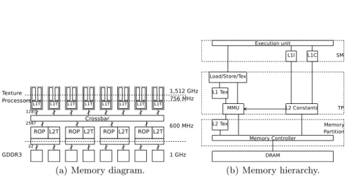
The unified architecture proposed by the DirectX 10 standard has been im-plemented in hardware since the release of the NVIDIA GeForce 8. An exam-ple of this architecture is depicted in Figure 1. The GPU has its own memory which bandwidth is usually an order of magnitude higher than system memory bandwidth. The graphics processor is seen as a set of multiprocessors. Each mul-tiprocessor consists in numerous processing elements (PEs) operating in SIMD.
3
(a) Memory diagram. (b) Memory hierarchy.
Fig. 1. Diagram of G92 architecture.
At each clock cycle, all the PEs in a multiprocessor execute the same instruc-tion sequence, but operate on different data. These multiprocessors incorporate various types of memory such as a register file, a scratchpad memory shared by all the PEs in a SIMD block, and read-only constant cache and texture cache. In addition, PEs can also read or write global memory available on the graphic card.
The GeForce 8 has a shared cached constant memory accessible in broadcast mode only, a global memory accessible with coalescing (with additional align-ment constraints), and a shared memory that allows coalesced, broadcast, and other patterns. Memory accesses that do not match these patterns are replaced by as many serial accesses as necessary, resulting in decreased performance. For example, the Tesla C870 embeds 1.5 GB of global memory with a peak band-width of 77 GB/s, which is more than 10 times the bandband-width available between a CPU and system memory. Multiprocessors integrate various computational units in order to implement the functionalities offered by the shaders: general computational units with embedded multiply-accumulators, texturing and filter-ing units, a dedicated unit to evaluate mathematical functions (e.g., sine, cosine, reciprocal, and reciprocal square root), and attribute interpolation units. Com-putational units can handle integer and floating-point arithmetic and there is no overhead associated with mixing both operations. Each multiprocessor of the GeForce 8 is able to execute a warp of 32 floating-point additions, multiplica-tions, multiply-and-adds or integer addimultiplica-tions, bitwise operamultiplica-tions, comparisons, minimum or maximum of 2 numbers in 4 clock cycles. As there is no 32-bit in-teger multiplication in hardware, evaluating such an operation requires 16 clock cycles for a warp. For instance, one GPU of the GeForce 9800GX2, depicted in Figure 1, has 16 multiprocessors and each SIMD block is composed of 8 PEs and 2 functional evaluation units.
3
Measurement and Tests Description
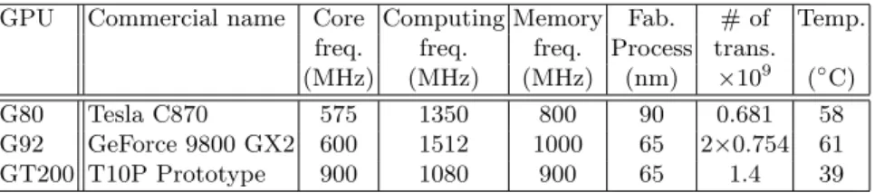
We measure the power consumption of several Nvidia graphics card supporting the CUDA API described in Table 1. This includes a Tesla C870 card used for scientific computing, a dual GPU high-end graphics card 9800 GX2 and a T10P compute processor engineering sample.
GPU Commercial name Core Computing Memory Fab. # of Temp. freq. freq. freq. Process trans. (MHz) (MHz) (MHz) (nm) ×109 (◦
C) G80 Tesla C870 575 1350 800 90 0.681 58 G92 GeForce 9800 GX2 600 1512 1000 65 2×0.754 61 GT200 T10P Prototype 900 1080 900 65 1.4 39
Table 1. Main characteristics of the tested graphic cards. Frequencies of the GPU, computational units and memory are given, as well as the manufacturing process, the number of transistor and the temperature provided by the integrated sensor.
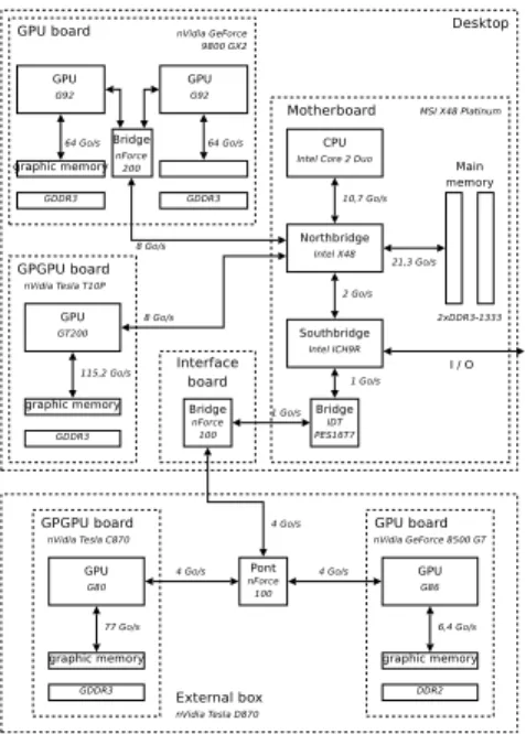
The considered GPUs are tested in a desktop environment with a MSI X48 Platinum motherboard, an Intel Core 2 Duo E8400 processor with 6 MB L2 cache running at 3 GHz, four 1GB Corsair TWIN3X2048-1333C9DHX DDR3-1333 9-9-9-24 memory modules, and a 750 W Corsair HX750W power supply. This configuration is described in Figure 2. Our motherboard based on an X48 Intel chipset offers two PCI-e x16 2.0 and two PCI-e x4 1.0 slots through a bridge. The tested GPUs are included in a separated Tesla D870 box connected to the system through a dedicated bridge (NForce 100). Our software configuration uses Linux Ubuntu 8.04, with CUDA 2.0 and proprietary graphic drivers Nvidia 177.13.
To measure the power consumption we use a Tektronix TDS 3032 oscilloscope with the built-in analogue 20 MHz low-pass filter. The first input measures the current with a clamp sensor CA60, while the second measures voltage. The product of both measurements gives us the power consumption of the GPU through the external power. We took into consideration the power provided to the PCIe bus as well as the external power of the GPU. We noticed during our tests that the main source of power is provided by the external link, as during computation only 10 to 15 extra W are coming from the PCI bus.
We are aware that the measurements collected using this methodology are subject to caution. First, we not only measure the power consumption of the GPU but we also measure the power consumption of the whole board that in-cludes the GPU, the graphic memory, DC/DC voltage converters, and others ICs (bridge, video chipset, . . . ) However we assume that we will notice a dif-ference in the power consumption only if these parts are stressed. Secondly, we measure the consumption ahead of the board voltage regulators which include
5
Fig. 2. Overview of our test configuration.
small capacitors (decoupling). This means that the power consumption may be missestimated. We design short tests such that some variations in ambient tem-perature or the cooling system will not affect the results. Sampling rate is 50 kHz which allows us to measure the power consumption at task level but not at instruction level.
4
Results
4.1 Global Power Consumption
We measure the computation time and the average power required by common GPGPU algorithms (matrix transposition, matrix multiplication and cuBLAS) on 1024 × 1024 random matrices. The implementations of GPGPU algorithms used for these tests are the ones included in the Nvidia CUDA SDK 1.2. Results are reported in Table 2.
We observed during our tests that before the Linux driver was loaded, the GT200 was using around 20 W, which corresponds to the power saving mode, as officially claimed by Nvidia. Once the driver is loaded, the power consumption of the GT 200 rises to 51 W while idle. Surprisingly, we noticed that even though the GT200 includes low-power GDDR3 compared to the Tesla C870 and a smaller fabrication process, the GT200 requires more energy than the Tesla C870 to perform a naive or an optimized matrix transposition. As the energy depends on memory access patterns on data which are located in memory bank modulo
GPU Idle Trans. naive Trans. optimized MatMul cuBLAS sgemm PAvg T E PAvg T E PAvg T E PAvg T E
(W) (W) (ms) (J) (W) (ms) (J) (W) (ms) (J) (W) (ms) (J) G80 68 103 2.4 0.247 127 0.30 0.038 132 25 3.3 135 11.8 1.59 G92 71 94 3.66 0.344 105 0.45 0.047 117 23.3 2.73 122 11.4 1.39 GT200 51 73 4.11 0.300 83 0.50 0.042 114 13 1.48 113 7.44 0.84
Table 2. Average power consumption PAvg, computation time T and
corre-sponding energy E measured for the execution of common GPGPU algorithms (Naive and optimized matrix transposition, matrix multiplication, cuBLAS).
the bus width, the example choosen (matrix of size 1024) is in favor of the C870 with a bus width of 384 bits compared to the 512 bits of the GT200 that raise bank conflicts when accessing data. Nevertheless, the GT200 requires twice less energy than the G80 on the matrix multiplication or cuBLAS example. This suggests that memory access patterns play a major role from performance as well as power consumption perspectives.
4.2 Multiprocessor
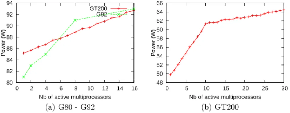
Considered GPUs integrate several multiprocessors with their own front-end: instruction fetch, decode, issue logic and execution units, etc. We run tests where the number of active multiprocessors varies from 1 to the maximum (16 for G80 and G92 and 30 for GT200). Results are reported in Figure 3. We observe that power consumption rise linearly with the number of multiprocessors up to respectively the maximum, one half and one third of the available multiprocessor for the G80, G92, GT200. This implies that the scheduling strategy for blocks to execute is different between the G80 and the G92 / GT200. We can deduce that the scheduling strategy for G92 and GT200 for blocks execution is to execute one block per group of texture processors which includes 2 multiprocessors for the G92 and 3 multiprocessors for the GT200. This means that the scheduling strategy of the G92 and GT200 is optimized for bandwidth usage, whereas the one used in the G80 is optimized for energy saving when the executed kernel is computationally bounded.
4.3 Execution Units
We measure the power consumption of various units within the GPU. We com-pare the power consumption of instructions predicated to true (that are really executed) and instructions that are predicated to false and we notice a significant variation. This means that instructions predicated to false are fetched, decoded but are not executed. This is unlike scalar architectures such as ARM or IA-64 behave, were predication is used to avoid pipeline stalls. On GPUs, predication is only used for SIMD control flow, while pipeline stalls are avoided using multi-threading. We measure the power used with various combination of units (MAD
7 80 82 84 86 88 90 92 94 0 2 4 6 8 10 12 14 16 Power (W) Nb of active multiprocessors GT200 G92 (a) G80 - G92 48 50 52 54 56 58 60 62 64 66 0 5 10 15 20 25 30 Power (W) Nb of active multiprocessors (b) GT200
Fig. 3. Power variations depending on the number of active multiprocessors.
units, MAD and MUL units, MAD and complex function evaluation units and double-precision unit). Results are reported in Table 4.
4.4 Memory Hierarchy
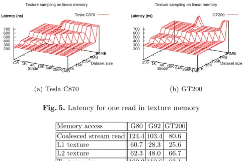
We measure how the memory hierarchy impacts the power consumption of GPUs. To measure the consumption, we developed a pointer chasing bench-mark to access each level of the memory hierarchy. This benchbench-mark includes a loop that traverses an integer array with various strides. 3 consecutive reads of one block of 128 bytes that will exploit coalescing are measured. Time is mea-sured using the internal cycle counter of one multiprocessor. Only one warp on one multiprocessor is used. The size of the array and the stride vary. In order to minimize measurement noise, the minimum values among 10 executions are reported. Results for memory latency are given in figure 4.
256 1K 4K 16K 64K256K1MB1K16K 256K4MB 64MB 200 300 400 500 600 700 Latency (ns) Stream reads Tesla C870 Stride Dataset size Latency (ns) (a) Tesla C870 256 1K 4K 16K 64K256K1MB1K16K 256K4MB 64MB 200 300 400 500 600 700 Latency (ns) Stream reads GT200 Stride Dataset size Latency (ns) (b) GT200
256 1K 4K 16K 64K256K1MB1K16K 256K4MB 64MB 200 300 400 500 600 700 Latency (ns)
Texture sampling on linear memory Tesla C870 Stride Dataset size Latency (ns) (a) Tesla C870 256 1K 4K 16K 64K256K1MB1K16K 256K4MB 64MB 200 300 400 500 600 700 Latency (ns)
Texture sampling on linear memory GT200
Stride
Dataset size Latency (ns)
(b) GT200
Fig. 5. Latency for one read in texture memory
Memory access G80 G92 GT200 Coalesced stream read 124.4 103.4 80.6 L1 texture 60.7 28.3 25.6 L2 texture 62.3 48.0 66.7 Texture miss 102.2 110.6 83.1
Table 3. Energy per memory request depending on where data is located. En-ergy results (nJ) per memory request of 128 bytes correspond to the measured power consumption divided by the measured bandwidth.
The observed latency for each GPU varies between 300 and 800 ns. In Figure 4.a (C870), we observe 3 steps at respectively 345 ns, 372 ns and 530 ns depending on the locality of the access. G92 behaves the same way with respective latencies of 325, 350 and 500 ns. We believe that these variations come from TLB hits and misses. Therefore, these results suggest a size of 4 KB per page with a 32-entry fully associative TLB. Results suggest that the second TLB level is accessed in 16 cycles on the G80 and G92 and 18 cycles on the GT200. However, our tests do not allow us to determine if it consists in an actual TLB or of a page table entry (PTE) cache. It is possible that it is shared with the second level of constant cache included in each texture processor. This cache may be used for instructions, constants, and PTEs.
DRAM is divided into pages that need to be precharged before each access and subsequently unloaded. According to our tests, DRAM page misses do not impact measured latency and power consumption. This may come from the fact that the memory controller optimizes page activation and unloading according to the address and type of memory access waiting in the buffer and that the access latency is made constant based on the worst case to simplify the design of the memory controller.
The latencies of texture memories are given in Figure 5. We observe the same steps as in Figure 4 plus the variation due to the two texture caches. By
9
comparing the latency of a cache miss in the texture cache with a memory read in the same conditions, we estimate at 30 to 50 cycles the overhead due to texture filtering and the extra cache access depending on the GPU generation. We also measured that the latency to access the L2 cache and to go through the memory crossbar should be between 35 and 50 cycles.
G80 G92 GT200 Operation # P CPI E P CPI E P CPI E
inst. (W) (nJ/warp) (W) (nJ/warp) (W) (nJ/warp) MAD 32 107 4.75 8.57 100 4.29 5.06 91 4.3 5.31 Pred 32 90 2.38 2.43 93 2.39 2.14 75 2.36 1.75 MAD+MUL 64 117 3.19 7.24 111 2.83 4.61 102 2.82 4.44 MAD+RCP 40 115 3.96 8.63 110 3.55 5.63 98 3.54 5.14 RCP 8 98 15.89 22.07 96 16 16.28 81 15.99 14.81 MOV 32 118 2.31 5.34 113 2.46 4.21 101 2.46 3.79
Table 4. Number of instructions, measured power P, number of cycles per in-struction and the energy required per warp for ALU operation on G80, G92 and GT200.
We measured the energy required for one memory request of 128 bytes exe-cuted by a warp on the G80, G92 and GT200 architectures. Results are reported in Table 3. The G80, G92 and GT200 are respectively made of 16, 16 and 30 mul-tiprocessors. Kernels used for the tests are launched with 512 threads/block with as many blocks as multiprocessors. The instruction count reflects the number of operations that can be executed in a single warp. The measured power corre-sponds to the average power measured during the whole computation. CPI gives the number of clock cycles per instruction which corresponds to the number of clock cycles measured with the internal cycle counter divided by the number of threads per block. The energy per warp corresponds to extra power required to perform a specific operation for a warp multiplied by the computational time. We observe that the L1 texture cache of the G80 requires the same amount of energy per byte as the L2 texture cache. This is certainly due to the small bandwidth performance of the L1 texture cache (76 GB/s for L1 and L2 texture cache). However we cannot explain the small performance of the L2 texture cache of the GT200. The comparison of Table 3 and 4 leads to the conclusion that executing MAD is 7 to 15 times more energy efficient than accessing memory on a G80.
5
Conclusion
This article presents some measurements and an analysis on how computations and memory accesses impact the power consumption of some Nvidia GPUs (G80, G92, GT200) in the CUDA framework. Memory accesses can significantly de-grade the performance and power consumption such that the G80 may be a
better alternative than the latest GT200 in some specific cases. Our tests show how blocks of threads are dispatched among the multiprocessors when the num-ber of multiprocessors is larger than the numnum-ber of blocks and how it could negatively impact the power consumption for computationally bounded kernels. We also compare the energy required for various operations for a given warp with the energy required for a memory access and show that computations are up to 7 to 15 times more power efficient than memory accesses.
Our tests show that environmental conditions such as temperature and mea-surement equipment can impact the results by 10 to 15%. Therefore we are currently working on minimizing the impact of the environment by executing the same tests with others tools in a different environment. We also plan to measure the clock gating impact and perform comparisons between Nvidia and ATI GPUs for a given workload.
References
1. David Brooks, Vivek Tiwari, and Margaret Martonosi. Wattch: a framework for architectural-level power analysis and optimizations. SIGARCH Comput. Archit. News, 28(2):83–94, May 2000.
2. C. Piguet, editor. Low-Power Electronics Design. Number 1941 in Computer Engi-neering. CRC Press, November 2004.
3. Ruchira Sasanka, Sarita V. Adve, Yen-Kuang Chen, and Eric Debes. The energy efficiency of cmp vs. smt for multimedia workloads. In ICS ’04: Proceedings of the 18th annual international conference on Supercomputing, pages 196–206, New York, NY, USA, 2004. ACM.
4. E. Senn, J. Laurent, N. Julien, and E. Martin. SoftExplorer: Estimating and op-timizing the power and energy consumption of a C program for DSP applications. EURASIP Journal on Applied Signal Processing, pages 2641–2654, January 2005. 5. N.H.E. Weste and D. Harris. CMOS VLSI Design: A Circuits and Systems
Per-spective. Addison Wesley, third edition, 2005.
6. W. Ye, N. Vijaykrishnan, M. Kandemir, and M. J. Irwin. The design and use of simplepower: a cycle-accurate energy estimation tool. In DAC ’00: Proceedings of the 37th conference on Design automation, pages 340–345, New York, NY, USA, 2000. ACM.