HAL Id: hal-03022574
https://hal.archives-ouvertes.fr/hal-03022574
Submitted on 24 Nov 2020
HAL is a multi-disciplinary open access
archive for the deposit and dissemination of
sci-entific research documents, whether they are
pub-lished or not. The documents may come from
teaching and research institutions in France or
abroad, or from public or private research centers.
L’archive ouverte pluridisciplinaire HAL, est
destinée au dépôt et à la diffusion de documents
scientifiques de niveau recherche, publiés ou non,
émanant des établissements d’enseignement et de
recherche français ou étrangers, des laboratoires
publics ou privés.
Operation of near-field scanning millimeter-wave
microscopy up to 67 GHz under scanning electron
microscopy vision
P Polovodov, Didier Theron, S. Eliet, V Avramovic, C Boyaval, Dominique
Deresmes, G Dambrine, K. Haddadi
To cite this version:
P Polovodov, Didier Theron, S. Eliet, V Avramovic, C Boyaval, et al.. Operation of near-field scanning
millimeter-wave microscopy up to 67 GHz under scanning electron microscopy vision. IEEE MTT
International Microwave Symposium, IMS 2020, Aug 2020, Los Angeles (On-line event ), United
States. �10.1109/IMS30576.2020.9224090�. �hal-03022574�
Operation of Near-Field Scanning Millimeter-wave Microscopy up to
67 GHz under Scanning Electron Microscopy Vision
P. Polovodov, D. Théron, S. Eliet, V. Avramovic, C. Boyaval, D. Deresmes, G. Dambrine and K. Haddadi
Univ. Lille, CNRS, UMR 8520 - IEMN, F-59000 Lille, France
kamel.haddadi@univ-lille.fr
Abstract—A near-field scanning millimeter-wave microscope is
developed with broadband capabilities up to 67 GHz. The instrumentation has been designed to operate inside a scanning electron microscope for environment control and water meniscus elimination. Scanning electron microscopy imaging of the tip / sample interaction gives the unique possibility to limit the scan area and preserve the integrity of the probe tip. In addition, hybrid imaging considering simultaneously atomic, microwave and electron microscopy tools is beneficial for further modeling to address the quantitative characterization of nanomaterials. Experimental data are exemplary shown to demonstrate the viability of the solution proposed.
Keywords—RF nanotechnology, near-Field scanning
microwave microscopy (NSMM), atomic force microscopy (AFM), scanning electron microscopy (SEM), millimeter-wave.
I. INTRODUCTION
The introduction of near-field scanning microwave microscopy (NSMM) tools have pioneered many applications, notably including mapping and quantitative measurement of the electrical properties of materials and devices at micro and nanoscale [1]. Basically, the near-field scanning microwave microscope (NSMM) consists of an atomic or scanning tunnelling microscope combined with a vector network analyzer (VNA) [2]-[5]. The tip scans across the sample, emitting a microwave signal scattered by the material, altering its amplitude or/and phase properties [6].
There is an urgent need to extend the frequency capabilities of microwave microscopy tools to achieve repeatable and traceable measurement data [7]-[10]. Indeed, water meniscus in the vicinity of the probe tip and material surface alter the measurement quality and remains difficult to be modelled accurately [11]. In this effort, a novel instrumentation has been thought and built from scratch [12]-[13]. The instrumentation has been designed to operate inside a scanning electron microscope (SEM) for environment control and water meniscus elimination [14]-[15]. This NSMM is developed with broadband capabilities up to 67 GHz in vacuum environment, and up to 110 GHz in air.
II. INSTRUMENTATION DEVELOPMENT
A. Millimeter-wave NSMM probing structure
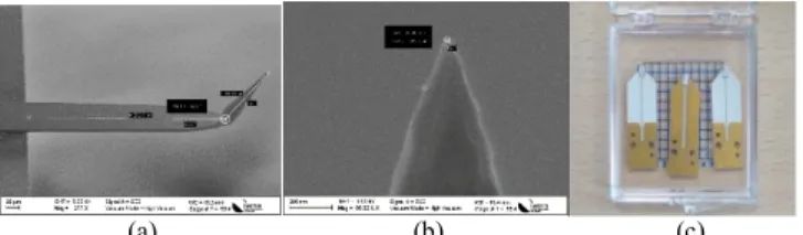
The NSMM-cantilever consists of a modified 25Pt300B microwave probe from Rocky Mountain Nanotechnology® (RMN) with sub-20 nm apex radius to achieve 67 GHz frequency operation [Fig. 1(a) and Fig. 1(b)]. The probe has been redesigned to support a transverse electromagnetic mode (TEM) through a propagating microstrip structure. This new
NSMM-Cantilever is fed by a coaxial cable itself connected to the microwave measurement system, i.e. VNA. Consequently, a dedicated coaxial to microstrip transition built up with two parts has been developed. In particular, the cantilever is embedded into a waveguide structure (both coplanar and microstrip structures have been realized for further comparisons) which can be exchanged in case of destroyed tips by using a solder-less PCB mount 1.85 mm connector of Rosenberger Corp. with a clamping and screwing mechanism [Fig. 1(c)]. The NSMM-probes have been assembled and millimeter-wave characterization has been checked using a VNA (not shown here).
(a) (b) (c)
Fig. 1 (a) Scanning electron image of the cantilever (probe 25Pt300D). (b) Zoom of the apex size with measured diameter around 26 nm. (c) Cantilever probe mounted on dedicated PCB for frequency operation up to 67 GHz.
B. AFM instrumentation
The atomic force microscopy (AFM) is realized by considering the general deflection laser approach. To that end, a fiber-coupled laser source Fabry-Perot 635 nm 2.5 mW from Thorlabs® is used to generate the laser signal. A Fixed Focus Collimation Packages (FC/PC) connector F280FC-B from Thorlabs® (beam diameter = 3.4 mm, focal length = 18.24 mm) is used to collimate the signal from output from the single mode fiber (Fig. 2). A feedthrough passage is considered for the connection of the optical fiber in the SEM. A quadrant photodiode referenced QD50-0-SD from OSI Optoelectronics® with associated circuitry is used to provide two difference signals and a sum signal.
Fig. 2 Design of the laser deflection system for AFM implementation.
C. Sample holder and temperature control
The sample stage is composed of an AFM scanner positioned onto a coarse positioning stage [Fig. 3(a)]. The positioning stage consists of three piezo driven linear actuators
manufactured by Smaract GmbH® with scanning ranges of 26 mm in X and Y directions and 11 mm in Z direction. The actuators enable closed-loop operation with less than 10 nm resolution and 25 nm repeatability in any direction. The AFM scanner ANSxyz100hs from Attocube® operates in open-loop on scanning ranges of 50×50×24 µm3 with sub-nm positioning
resolution and 0.1% scan repeatability [Fig. 3(b)]. A heating element and thermal probe from Attocube® are integrated to the sample stage for temperature control [Fig. 3(c)].
(a) (b) (c)
Fig. 3 (a) Sample scanning stage. (b) Sample holder. (c) Heating element and probe integrated in the sample holder.
One major value of the solution proposed is to maintain all the microwave parts (NSMM-probe and coaxial cable) fixed during scanning operation.
D. System integration and automation
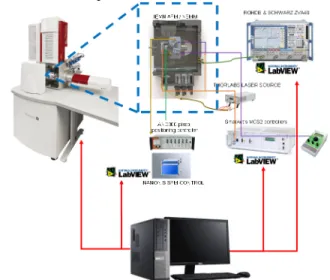
The NSMM has been integrated into a SEM Tescan® MIRA XMU. This latter is a high performance SEM system that features a high brightness Schottky emitter for achieving high resolution and low-noise imaging. It has the advantage of delivering fast image acquisition, an ultra-fast scanning system, dynamic and static compensation and built-in scripting for user-defined applications. The hemisphere above the sample is mainly occupied by the electron column and leaves only a very small gap accessible for the NSMM to achieve a working distance of 20 mm. The NSMM stage is mounted on the chamber vertically to the electron beam of the SEM.
Fig. 4 NSMM integrated in the SEM Tescan® MIRA XMU. The electron gun of the SEM is focused on the probe tip contacting the sample.
E. Measurement modes with nano-robotics and Labview®
In contrast with conventional NSMM operating in air, the manual adjustment of the laser beam is not possible in the SEM. Consequently, both the laser beam and detector are mounted on XYZ piezo-driven nano-positionning stages (Fig. 4). A dedicated LabVIEW® software is used for fine adjustments. This software controls the sample stage (both SmartAct® and Attocube® stages) and the VNA settings (input power, number of points, intermediate frequency bandwidth IFBW, frequency of operation). XY and Z scanning routines provide both AFM
and microwave data. The Attocube® scanner is based on the NANONIS® SPM platform.
Fig. 5 Configuration of the NSMM in SEM interfacing the SEM Tescan MIRA XMU, a Rhode & Schwarz® ZVA VNA (or equivalent Keysight® VNA), ATTOCUBE® and SmarAct® positioning stages.
III. EXPERIMENTAL VALIDATION
The performances of the system considering different measurements configurations have been tested and validated.
A. Microwave imaging of sub-fF (10-15 F)
metal-oxyde-semiconductor (MOS) capacitors reference kit
The reference kit used here was developed by Keysight®
and MC2-Technologies®. It consists of MOS capacitors the
values of which range from 0.1 fF to 4 fF [16]-[17]. The MOS capacitors are composed of circular gold electrodes evaporated on silicon dioxide deposited on a P-type silicon substrate of resistivity
1–3 Ωcm or 0.01 Ωcm. In order to vary the capacitances values, the diameter of the upper gold pad varies from 1 to 4 μm and the Silicon oxide (SiO2) thickness ranges from 50 to 300 nm
with about 80 nm steps. The impedance of the MOS structures measured at the tip apex of the probe can be modelled by an oxide capacitance Cox. The capacitance Cox is calculated from
the areas of the gold pads and the SiO2 thicknesses. The
thickness and areas of the capacitors were estimated from the AFM topography measurements [Fig. 6(a)] to take into account any deviations in geometry induced by the fabrication process of the reference kit. The measured thicknesses dox of the SiO2
layers were 82 nm, 150 nm, and 211 nm [Fig. 6(b)]
(a) (b)
Fig. 6 (a) Atomic force microscopy image of the MOS capacitances reference kit. (b) Extracted 1D profiles at two different Y positions for thickness measurement of the SiO2 layers.
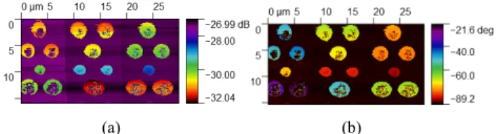
The microwave images of the amplitude and phase-shift of the complex reflection coefficient have been measured using a VNA at the test frequency around 7.59 GHz with low input RF power of -25 dBm and IFBW set to 100 Hz. To enhance the measurement sensitivity, a home-made microwave interferometer built up with a power combiner, two directional couplers, a variable attenuator and two low noise amplifiers (LNA) in series with total gain of 30 dB has been considered. The resulting microwave images of the reference calibration kit are given in Fig. 7. From these data, a variation of around 6 dB and 77 degrees are noticed for the amplitude and phase-shift images respectively.
(a) (b)
Fig. 7 (a) Amplitude and (b) phase-shift images of the complex reflection coefficient considering the MOS capacitors reference kit – f ≈ 7.59 GHz, RF power = -25 dBm, IFBW = 100 Hz.
From these data, the amplitude of the reflection coefficient (note: The reflection coefficient is denoted S21 as the
measurement considering the interferometric set-up is done in transmission mode) as a function of the theoretical capacitance is plotted in Fig. 8.
Fig. 8 Measured amplitude signal as a function of the theoretical capacitance value (device under test = MOS capacitors reference kit) – f ≈ 7.59 GHz, RF power = -25 dBm, IFBW = 100 Hz.
After this preliminary benchmark, fine experimental analysis is proposed in the following to highlight the unique advantages offered by the simultaneous combination of AFM, NSMM and SEM tools.
B. Towards unique hybrid analysis platform for data fusion
An intensive measurement campaign has been considered to qualify the new instrumentation proposed. For sake of clarity, we report only some results highlighting the interest of operation inside a SEM. In contrast with conventional NSMM, the solution proposed allows a real time visualization of both the probe and the sample under investigation. Consequently, we demonstrate a fine positioning of the probe on the position of interest to be characterized (Fig. 9). Consequently, the imaging of the full device under test is not needed as the area of interest is located preliminary by SEM. This results in optimized measurement protocol while preserving the integrity of the probe.
Figure 9 (a) Scanning electron microscopy image of the probe approaching the sample under test. (b) probe in contact with the sample. (c) Zoom of the probe apex in contact with the sample.
The unique capability of the new instrument to provide hybrid data for fine analysis is demonstrated in this part. To that end, the reference calibration kit is considered as device under test (DUT). Fig. 10 shows different steps of the landing of the probe on the DUT. We target a 1D profile measurement of the capacitor illustrated in Fig. 10(d).
(a) (b) (c) (d) Fig. 10 Scanning electron microscopy (SEM) images of the probe landing on the MOS capacitors calibration kit.
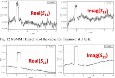
One of the major impact of the solution proposed is to increase the frequency of operation to concentrate the electrical fields at the probe apex. The resulting benefits are the the measurement sensitivity. Consequently, we have considered two test frequencies, i.e. 3 GHz and 30 GHz corresponding to free-space wavelengths of 10 cm and 1 cm respectively. To evaluate the impact of the operating frequency, no interferometric set-up is considered in these experiments. The signal to noise ratio (S/N) is enhanced by increasing the input RF power to 0 dBm and by considering a low IFBW of 10 Hz. The 1D AFM profile together with the related SEM image of the probe / capacitor are given in Fig. 11.
Fig. 11 AFM and SEM (inset of the graph) images of a MOS capacitor. The capacitor diameter of ~3 µm is obtained by 1D fitting using Gwyddion® software
From these results, we can correlate the SEM and AFM images. Indeed, the deterioration seen at the edge of the capacitor on the
SEM image results in diminution of the height seen on the AFM topography. In the same manner, the existence of an impurity on the gold patch of the capacitor seen on the SEM image results on a localized increase of the AFM topography. The corresponding microwave images of the real part and imaginary part of the complex reflection coefficients measured at 3 and 30 GHz are given in Fig. 11 and Fig. 12 respectively. The results obtained demonstrate the interest of operating in the millimeter-wave regime. In particular, the S/N is clearly enhance when considering the measurements taken at 30 GHz. Both real and imaginary parts reveal a sensitivity enhanced by a factor of about 10 between the test frequencies. When comparing the AFM and NSMM images, a loss of contact is found for about half of the capacitor. Indeed, the MOS capacitor gold patches can present a contaminated surface resulting in bad electrical contact that has already been described in the literature. Consequently, the frequency diversity offered by the instrument is an advantage to discriminate the variations of the microwave impedances due to the local surface property variations from those attributed to non-systematic errors.
Fig. 12 NSMM 1D profile of the capacitor measured at 3 GHz.
Fig. 12 NSMM 1D profile of the capacitor measured at 30 GHz. IV. CONCLUSION
Scanning microwave microscopy is becoming an established technique for tackling the frontier between electrical wavelengths and nanoscale dimensions. In this effort, first demonstration of atomic force and millimetre-wave imaging inside a SEM has been successfully achieved. In particular, we demonstrate collimation of the electric fields in the vicinity of the probe apex when operating with millimetre-wave excitation millimetre-wavelengths, resulting in enhanced electrical sensitivity. Future works are clearly oriented towards establishing traceability of scanning microwave microscopy by accurate environment control and FEM modelling of the probe tip / material interaction using SEM vision
ACKNOWLEDGMENT
This work has received funding from the European Union Horizon H2020 Programme (H2020-NMBP07-2017) under grant agreement n°761036 MMAMA. This work used the facilities within the EQPX ExCELSiOR (www.excelsior-ncc.eu) funded by the National Research Agency (ANR).
REFERENCES
[1] S. M. Anlage, V. V. Talanov, and A. R. Schwartz, “Principles of near-field microwave microscopy,” Scanning Probe Microscopy: Electrical
and Electromechanical Phenomena at the Nanoscale, S. Kalinin and A. Gruverman, Eds. New York, Springer Sci., pp. 215–253, Aug. 2007.
[2] S. Fabiani, D. Mencarelli, A. Di Donato, T. Monti, G. Venanzoni, A Morini, T. Rozzi, and M. Farina, “Broadband Scanning Microwave Microscopy investigation of graphene”, Proc. IEEE MTT-S International
Microw. Symp., pp. 1-4, June 2011.
[3] M. Farina, D. Mencarelli, A. Morini, L. Pierantoni, X. Jin and J. Hwang, "Developments of microwave microscopy for application to biological samples," 2017 International Conference on Manipulation, Automation
and Robotics at Small Scales (MARSS), Montreal, QC, 2017, pp. 1-5.
[4] G. Fabi et al., "Inverted Scanning Microwave Microscopy for Nanometer-scale Imaging and Characterization of Platinum Diselenide," 2019 IEEE
MTT-S International Microwave Symposium (IMS), Boston, MA, USA,
2019, pp. 1115-1117.
[5] J. Li, Z. Nernati, K. Haddadi, D. C. Wallace and P. J. Burke, "Scanning Microwave Microscopy of Vital Mitochondria in Respiration Buffer,"
2018 IEEE/MTT-S International Microwave Symposium - IMS,
Philadelphia, PA, 2018, pp. 115-118.
[6] G. Gramse, M. Kasper, L. Fumagalli, G. Gomila, P. Hinterdorfer and F. Kienberger, “Calibrated complex impedance and permitivity measurements with SMM,” Nanotechnology, vol. 25, no. 14, p. 8, 2014. [7] L. Zhang, Y. Ju, A. Hosol and A. Fujimoto, “Microwave atomic force
microscopy imaging for nanometer-scale electrical property characterization,” Review of Scientific Instruments, vol. 81, no. 12, pp. 123708, 2010.
[8] A. Imtiaz, T. M. Wallis and P. Kabos, "Near-Field Scanning Microwave Microscopy: An Emerging Research Tool for Nanoscale Metrology”,
IEEE Microwave Magazine, vol.15, no.1, pp.52-64, Jan. 2014.
[9] S. Berweger et al., "Near-field microwave microscopy of one-dimensional nanostructures," 2016 IEEE MTT-S International
Microwave Symposium (IMS), San Francisco, CA, 2016, pp. 1-3.
[10] Oxford Instruments, Inc., “Scanning Microwave Impedance Microscopy (sMIM)”, Datasheet, 2014.
[11] M. Calleja, M. Tello and R. Garcia, “Size determination of field-induced water menisci in noncontact atomic force microscopy,” Journal of applied
physics, vol. 92, no. 9, pr. 5539-5542, 2002.
[12] K. Haddadi, O. C. Haenssler, C. Boyaval, D. Theron and G. Dambrine, "Near-field scanning millimeter-wave microscope combined with a scanning electron microscope," 2017 IEEE MTT-S International
Microwave Symposium (IMS), Honololu, HI, 2017, pp. 1656-1659.
[13] K. Haddadi et al., "Combined scanning microwave and electron microscopy: A novel toolbox for hybrid nanoscale material analysis,"
2017 IEEE MTT-S International Microwave Workshop Series on Advanced Materials and Processes for RF and THz Applications (IMWS-AMP), Pavia, 2017, pp. 1-3.
[14] K. Haddadi, P. Polovodov, D. Théron and G. Dambrine, "Quantitative Error Analysis in Near-Field Scanning Microwave Microscopy," 2018
International Conference on Manipulation, Automation and Robotics at Small Scales (MARSS), Nagoya, 2018, pp. 1-6.
[15] P.Polovodov, O. C. Haenssler, D. Théron, C. Boyaval, S. Eliet, G. Dambrine, and K. Haddadi "Building a near-field scanning millimeter-wave microscope integrated in a scanning electron microscope", 2019
International Conference on Manipulation, Automation and Robotics at Small Scales (MARSS), Helsinki, Finland, July 2019.
[16] T. Dargent, K. Haddadi, T. Lasri, N. Clément, D. Ducatteau, Bernard Legrand, H. Tanbakuchi, and D. Theron. "An interferometric scanning microwave microscope and calibration method for sub-fF microwave measurements." Review of Scientific Instruments, vol. 84, no. 12, p. 123705, 2013.
[17] K. Haddadi, C. Brillard, G. Dambrine and D. Théron, "Sensitivity and accuracy analysis in scanning microwave microscopy," 2016 IEEE
MTT-S International Microwave MTT-Symposium (IMMTT-S), MTT-San Francisco, CA, 2016,