HAL Id: hal-00842763
https://hal.archives-ouvertes.fr/hal-00842763
Submitted on 9 Jul 2013HAL is a multi-disciplinary open access archive for the deposit and dissemination of sci-entific research documents, whether they are pub-lished or not. The documents may come from teaching and research institutions in France or abroad, or from public or private research centers.
L’archive ouverte pluridisciplinaire HAL, est destinée au dépôt et à la diffusion de documents scientifiques de niveau recherche, publiés ou non, émanant des établissements d’enseignement et de recherche français ou étrangers, des laboratoires publics ou privés.
Structural and optical properties of (In,Ga)As/GaP
quantum dots and (GaAsPN/GaPN) diluted-nitride
nanolayers coherently grown onto GaP and Si substrates
for photonics and photovoltaics applications
Olivier Durand, Cédric Robert, Thanh Tra Nguyen, Samy Almosni, Thomas
Quinci, Jithesh Kuyyalil, Charles Cornet, Antoine Létoublon, Christophe
Levallois, Jean-Marc Jancu, et al.
To cite this version:
Olivier Durand, Cédric Robert, Thanh Tra Nguyen, Samy Almosni, Thomas Quinci, et al.. Struc-tural and optical properties of (In,Ga)As/GaP quantum dots and (GaAsPN/GaPN) diluted-nitride nanolayers coherently grown onto GaP and Si substrates for photonics and photovoltaics applications. Proceedings of SPIE, the International Society for Optical Engineering, SPIE, The International So-ciety for Optical Engineering, 2013, Quantum sensing and nanophotonic devices X, 8631, pp.863126. �10.1117/12.2012670�. �hal-00842763�
Structural and optical properties of (In,Ga)As/GaP quantum dots and
(GaAsPN/GaPN) diluted-nitride nanolayers coherently grown onto
GaP and Si substrates for photonics and photovoltaics applications
O.Durand
1, C. Robert1, T. Nguyen Thanh
1, S. Almosni
1, T. Quinci
1,2, J. Kuyyalil
1, C. Cornet
1, A.
Létoublon
1, C. Levallois
1, J.-M. Jancu
1, J. Even
1, L. Pédesseau
1, M. Perrin
1, N.Bertru
1, A. Sakri
1, N.
Boudet
3, A. Ponchet
4, P. Rale
5, L. Lombez
5, J.-F. Guillemoles
5, X. Marie
6, A. Balocchi
6, P. Turban
7,
S. Tricot
7, Mircea Modreanu,
8S. Loualiche,
1A. Le Corre
11
Université Européenne de Bretagne, INSA, FOTON-OHM, UMR 6082, F-35708 RENNES, France
2INES – CEA, 50, avenue du lac Léman Savoie Technolac, 73370 Le Bourget-du-Lac, France
3
CRG-D2AM, ESRF & Inst. Néel, CNRS-UJF, 25 Av des Martyrs, 38042 Grenoble, France
4CEMES-CNRS, Université de Toulouse, 29 rue J. Marvig BP 94347, 31055 Toulouse Cedex 4,
France
5
IRDEP, UMR 7174 - CNRS-EDF-ENSCP,EDF R&D, 78401 Chatou Cedex, France
6Université de Toulouse, INSA-CNRS-UPS, LPCNO, 135 avenue de Rangueil, 31077 Toulouse,
France
7
Equipe de Physique des Surfaces et Interfaces, Institut de Physique de Rennes UMR UR1-CNRS
6251, Université de Rennes 1, F-35042 Rennes Cedex, France.
8
Tyndall National Institute-University College Cork, Lee Maltings, Prospect Row, Cork, Ireland
ABSTRACT
Lattice-matched GaP-based nanostructures grown on silicon substrates is a highly rewarded route for coherent integration of photonics and high-efficiency photovoltaic devices onto silicon substrates. We report on the structural and optical properties of selected MBE-grown nanostructures on both GaP substrates and GaP/Si pseudo-substrates. As a first stumbling block, the GaP/Si interface growth has been optimised thanks to a complementary set of thorough structural analyses. Photoluminescence and time-resolved photoluminescence studies of self-assembled (In,Ga)As quantum dots grown on GaP substrate demonstrate a proximity of two different types of optical transitions interpreted as a competition between conduction band states in X and Γ valleys. Structural properties and optical studies of GaAsP(N)/GaP(N) quantum wells coherently grown on GaP substrates and GaP/Si pseudo substrates are reported. Our results are found to be suitable for light emission applications in the datacom segment. Then, possible routes are drawn for larger wavelengths applications, in order to address the chip-to-chip and within-a-chip optical interconnects and the optical telecom segments. Finally, results on GaAsPN/GaP heterostructures and diodes, suitable for PV applications are reported
Keywords: photonics on silicon, monolithic integration, GaP/Si, quantum dots, quantum wells, TEM and XRD, electroluminescence and photoluminescence, solar cells.
1. INTRODUCTION
Silicon microelectronics has been the engine of the modern information revolution for almost 50 years. In the never ending quest to process more and more data faster while using the smallest components, the silicon industry has successfully overcame many critical issues. The next key issue in the evolution of modern information system is to overcome the limitations of metal interconnects. The merger of photonics and
Invited Paper
Quantum Sensing and Nanophotonic Devices X, edited by Manijeh Razeghi, Eric Tournié, Gail J. Brown, Proc. of SPIE Vol. 8631, 863126 · © 2013 SPIE · CCC code: 0277-786X/13/$18 · doi: 10.1117/12.2012670
electronics into a dual-function platform, the optoelectronic integrated circuit (OEIC), fabricated using existing silicon infrastructure, has the potential to overcome this critical issue while pushing forward silicon-based microelectronics beyond the classical CMOS era [1-3]. Thus the OIEC platform brings new functionality useful for faster communication between circuit boards, chips on a board, and even different cores on a processor while not hindered by any problems associated with electromagnetic interference. In this context, the monolithic integration of a laser, based on III-V materials, and the compatibility with the current processing of electronic integrated circuits based on Si technology, remains the main stumbling block [4]. One of the most prominent issues comes from the large lattice mismatch existing between usual III-V materials (GaAs, InP) and Si which leads to the formation of highly defective III-V layers with consequently poor optical properties [5]. This issue can be overcome by adopting a pseudomorphic approach, i.e. growing GaP-based lattice-matched compounds on Si [6-9]. However, though studies of the growth of the quasi lattice-matched GaP indirect compound semiconductor onto Si substrate have already been reported, integration on Si substrates remains a highly rewarded challenge. Moreover, GaP is an indirect bandgap compound and is therefore not suitable for most photonics applications. This issue is overcame by the growth of diluted-nitride GaPN-based compounds on the GaP/Si pseudo-substrates, since GaPN can be perfectly lattice-matched with Si, by means of an appropriate adjustment of the N content (a few percent). Indeed, GaPN ternary compounds have shown to develop a pseudo-direct-band gap character due to a large bowing effect, as a function of the N content, and therefore, can act as efficient light emitters [10;11]. Moreover, such heterostructure development is also driven by the elaboration of high performance multijunction solar cells onto the low-cost Si substrate [12].
We present the study of MQWs (Multi Quantum Wells) and Quantum Dots (QDs) coherently grown on either GaP substrates or GaP/Si pseudo-substrates as preliminary results toward the elaboration of laser devices on silicon substrates. Then, thorough structural analyses of the GaP/Si interface are reported, showing the presence of extended structural defects, that are Micro-twins (MTs) and AntiPhase Domains (APDs). Then, an evolution of these defects density is studied with respect to the growth conditions. Since the GaPN-based compounds emit at low wavelength, we propose an electronic band structure using materials compatible with the aforementioned compounds and suitable to emit at higher wavelengths, in order to address the chip-to-chip and within-a-chip-to-chip optical interconnects and the optical telecom segments. Finally, preliminary results on a diluted nitride MQWs diode on GaP shows promising result in the framework of a forthcoming elaboration of high-efficiency solar cells onto silicon substrates.
2. ACTIVE ZONE FOR LIGHT EMISSION: GA(IN)AS QDS
Quantum dots allow the coherent growth of small band gap material nanostructures with a larger lattice-mismatch than in the case of Quantum Wells. To this end, Ga(In)As quantum dots grown onto GaP substrates have been studied as light emitter zones, preliminary to their integration in lasers structures on silicon substrates. Moreover, their 0D confinement properties allow lower threshold currents than in their QWs counterparts [13]. Results on the binary InAs and GaAs compounds have already been reported and efficient Photoluminescence (PL) was not achieved to date either due to plastic relaxation for the large mismatched InAs QDs/GaP system [14;15], or due to strain relaxation processes and indirect band gap for the GaAs QDs/GaP [16]. Concerning the ternary GaInAs QDs compounds grown onto GaP, Fuchi et al. have measured a PL signal up to 77 K while pointing out the issue of In composition due to its well-known surfactant effect [17]. Moreover, Rivoire et al. have reported single emission of type I In0.5Ga0.5As/GaP QDs in a large In composition regime [18] while our group have also reported Room Temperature PL from GaInAs QDs/GaP in a low In composition regime [19;20]. In the following, structural and optical properties of GaInAs QDs are reported.
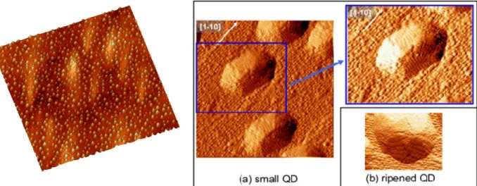
(a) small QD (b) ripened CD
2.1 Experimental details
Morphology measurements have been performed by Scanning Tunnelling Microscopy (STM) on Solid-Source Molecular Beam Epitaxy (SSMBE) made on (In,Ga)As QDs samples grown onto n-doped GaP(001) substrates.. While the nominal composition of indium was set to 30 %, the effective composition is expected to be lower than 15% due to the low In incorporation, depending on the strain [21].
Continuous wave PL and time-resolved PL have been performed on Gas-Source Molecular Beam Epitaxy (GSMBE) made on (In,Ga)As QDs samples grown onto n-doped GaP(001) substrates and capped with a 30 nm GaP layer preventing any surface non-radiative recombination.
Details of the growth conditions of both SSMBE and GSMBE samples can be found in references [19] and [20]. One has to notice that careful morphology analyses have been performed to ensure that both kinds of samples give similar features so that both morphology and PL results can be compared.
Photoluminescence experiments were carried out exciting samples with a 405 nm continuous-wave laser diode. The power density is roughly estimated to 80 W.cm-2. The samples were set in a helium bath closed-cycle cryostat to study PL from 10 K to room temperature.
Time-resolved photoluminescence spectroscopy has been carried out using a frequency-doubled Ti:Sapphire laser at the wavelength of 405 nm. The repetition rate was 80 MHz and the PL signal was analysed by a S20 streak camera. Measurements were performed at 10 K.
2.2 Structural analyses of the Ga(In)As QDs
Using STM analyses, the QDs density has been measured to be (1.3.1011±0.2. 1011) cm-2, Statistical analysis
of heights and radii distributions has also been performed, giving a mean QD height and a mean radius measured equal to (3.5±1.2) nm and 9.0±1.8 nm, respectively. This gives a typical aspect ratio (height to diameter ratio) of 0.2.
Fig. 1 : 800x800 nm² STM image of (In,Ga)As QDs
Fig. 2: (a) 60x60 nm² STM plane view of (In,Ga)As small QDs, not ripened. (b). ripened QDs.
STM high resolution measurement of the surface morphology is reported in fig 1, where the surface topography image is derived to enhance contrast. First, In has been found in the wetting layer, demonstrating that the QDs grow in a Stranski-Krastanow mode, as expected. Moreover, this image reveal atomic sites with
2 x220 x40 1 x15 0. 350K 300K 260K 12K 1.4 1.6 1.8 2.0 2.2 Energy (eV)
high electronic density located on top of the QDs, characteristic of an enrichment in In of the top QDs surface, characteristic of the well-known In segregation phenomenon [22;23], leading to an inhomogeneous In composition inside the QDs [20]. Finally, STM analyses have revealed two QDs populations, as show in fig. 2: small QDs (Fig 2.a) with an in-plane anisotropic ratio (between length and width) of 1.5, and large and isotropic in-plane QDs, likely formed from small QDs by a ripening process.
2.3 Optical properties
Optical properties of the GaInAs QDs have been studied through temperature and time dependent photoluminescence.
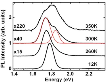
Fig. 3 : Temperature dependent PL spectra of (In,Ga)As/GaP QDs. The red thin lines show the fit of the two transitions by two Gaussian peaks
Fig.3 shows the variation of the PL from the GaInAs QDs with respect to the temperature, ranging from 12 K to 375 K. At low temperature, the PL spectrum displays a single peak centered at 1.78 eV (697 nm) with a full width at half maximum (FWHM) equal to 97 meV, characteristic of the dots size distribution. The temperature increase causes a classical red shift of the main peak to 1.74 eV at room temperature. However, a shoulder appears at around 160 K, on the high energy side of the PL spectrum, confirmed at Room Temperature (RT) by a clear peak characteristic of a Higher Energy (HE) second optical transition localised at 100 meV from the low energy (LE) peak. When increasing the temperature above 300 K, the maximum of PL intensity switches from the LE transition to the HE transition. Moreover, above RT, a decrease of the overall PL intensity has been observed, likely due to activation of non-radiative channels. Moreover, it has been shown that the HE optical transition is radiatively more efficient than the LE one. Supported by theoretical calculations of the band structure involving a combination of k.p and TB models, this PL behaviour has been interpreted as an indirect type of the ground optical followed by a second optical transition, present at room temperature, which could be of direct type [20]. The calculations have been done under the assumption the QDs In content is below 15 %. At room temperature, electrons get enough thermal energy to partially fill a Γ state and thus a more efficient optical transition (HE) is observed.
Time-resolved PL spectroscopy has also been performed to analyse the dynamics of the carrier recombination. Two different excitation power densities have been used: 70 W.cm-2 for the low power case
(LP) and 4000 W.cm-2 for the high power case (HP). Figure 4 shows the variations of the PL signal of both
790nm
.11
Ons ins 2ns 620nm 705nm 790nm1.00
0.75 0.50 0.250.00
8 e =o4
° °oA%:, euciag88m8holf°9:6 8ows°ol0aóo
LP - ELE HP - ELE HP - EHE 0 500 1000
Time (ps)
1500HE and LE peaks. A long decay time of the QDs emission energy has been measured with the LP density. This long decay time is independent of the emission energy, which is greater than the repetition period of the laser (12 ns), in agreement with the interpretation in terms of a LE ground transition corresponding to an indirect type transition. The PL spectrum broadens on the high energy side in the HP excitation density regime (fig 4.b). The decay time depends now on the emission energy with a shortening on the high energy side.
Fig. 4 : Streak camera image of time-resolved photoluminescence at 10 K for an excitation density of a) LP=70 W.cm-2 and b) HP=4000 W.cm-2. The white horizontal dashed line marks the instant of the laser pulse.
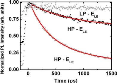
Fig. 5: PL dynamics at selected energies (ELE=1.76 eV and EHE=1.86 eV, shown by arrows on previous figure) for two power
densities (LP=70 W.cm-2 and HP=4000 W.cm-2). Red lines show biexponential fits.
Fig.5 shows the time-resolved PL intensity on two detection energies: ELE=1.76 eV and EHE=1.86 eV. For the
LP case, the emission at EHE is not detectable. For the HP case, the time-resolved emission related to the LE
a)
b)
transition can be fitted by the sum of a short exponential decay with a lifetime of 770 ps and a constant associated with the very long lifetime of the indirect transition. The physical reason of the shortest time may be a result of many body effects such as Auger effects due to the high density of electron-hole pairs (above ten per QD). For the HE transition, the emission shows a biexponential decay with short lifetimes of 340 ps and 1700 ps respectively. While many body effects and energy relaxation should have an influence on the carriers dynamics [24], the likely direct-type of the optical transition associated to the EHE energy could be
another reason of short decay times observed in these experiments. 2.4 Conclusion
In conclusion, the (In,Ga)As/GaP QDs system shows efficient RT luminescence properties suitable for laser applications, around 1.8 eV. PL experiments are coherent with a ground transition of indirect type. A second optical transition is present at room temperature, which could be of direct type, in agreement with theoretical calculations.
For device applications, larger dots or with a high enough In content are necessary, because the first transition is expected to switch to direct type, according to theoretical calculations. Moreover, adding some nitride in a diluted regime in order to obtain (In,Ga)As(N)/GaP QDs, along with an appropriate In content, is expected to overcome bandlineups issue [25] and to lower the emission energy due to the huge bowing effect, in order to reach emission wavelength higher than 1.1 μm suitable for chip to chip and on-chip applications. Indeed, previous preliminary results from another group [26] have shown a 1.39 eV PL emission in InGaAsN/GaP QDs on GaP with, however, a large full width at half maximum (FWHM) (334 meV) interpreted as a large inhomogeneous distribution of the QDs, showing therefore that there is a room of improvement in such a diluted-nitride QDs system.
3. ACTIVE ZONE FOR LIGHT EMISSION: (GAASPN/GAPN)/GAP/SI NANOLAYERS
In this part, GaAsPN/GaPN diluted-nitride QWs structures grown on both GaP and Si substrates are studied for light emission applications. The incorporation of N has been obtained using a ADDON valved rf plasma N2 source which avoid any sample irradiation from charged species known to introduce numerous point defects during the sample growth. Details of the MBE growth can be found in reference [27].
3.1 EL Experiments on (GaAsPN/GaPN) grown on GaP(001)
In previous papers, we have shown efficient RT EL of GaAsPN/GaPN QWs-based LEDs grown on n-doped GaP substrate. Active areas were in both cases grown on between two 300nm thick doped-GaP layers with a dopant concentration of 5.1018cm-3 (Si for n-type and Be for p-type). The MQW active area were composed of
five 2.7nm thick GaAs0.6975P0.2975N0.005 QWs separated by 30nm thick GaP0.995N0.005 barriers, with
concentrations estimated by high resolution X-ray diffraction (HRXRD) measurements. Then a 20nm thick GaP capping layer covers the heterostructure. All the actual thicknesses were measured using X-ray reflectometry [28]. Efficient RT EL was obtained at 1.7 eV in this heterostructure [27].
3.2 PL Experiments on (GaAsPN/GaPN) grown on Si(001)
A double GaAsPN/GaPN quantum wells has been grown on the GaP/Si virtual substrate for the study of optical properties [29]. The active area is located at 160nm away from the GaP/Si interface. As already
500 750 1000 1250
Time (ps)
1500
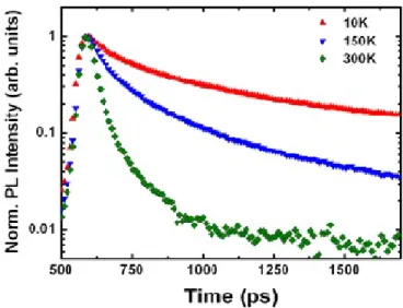
reported, a RT photoluminescence has been obtained on a 4°-off (001) silicon substrate from a GaAsPN/GaPN QWs structure grown on a GaP/Si pseudo substrate [29]. The incorporation of N in the (GaAsPN/GaPN) structure has been estimated around 1.2% and the incorporation of As has been determined equal to 70% by High Resolution X-ray Diffraction. The wavelength emission is centered at 820 nm at RT, close to the 850 nm wavelength required for telecommunication applications, such as datacoms. In the following, time-resolved PL measurements performed on the previous structure are reported. Fig 6 shows a luminescence decay following a non-single exponential behaviour, characteristic of disordered systems such as diluted nitride alloys [30]. However, decay times of 140ps and 1250ps at 10 K and of 30ps and 180ps at 300K, respectively, have been extracted using double exponential fits. Therefore, it has been deduced that the optical emission is likely due to efficient carrier injection in well-localised radiative centres at low temperature. These centres are separated by structural defects (non-radiative centers), thermally activated at higher temperature. This result shows that the optical limitation of the structure is likely due to the vicinity of the non-optimised GaP/Siinterface, to date, demonstrating that the obtaining of a defect free GaP/Si interface is a key issue for any further optical properties improvement.
Fig. 6 Time-resolved photoluminescence spectra of GaAsPN/GaPN QWs near (160 nm) the GaP/Si interface. The detection energy corresponds to the peak of the spectrum for a given temperature.
3.3 Conclusion
Efficient RT EL properties at 1.7 eV have been shown on GaAsP(N)/GaP(N) diluted-nitride QWs-based LEDs epitaxially grown onto GaP(001) substrates. Moreover, RT PL centered around 820 nm has been shown on a similar (GaAsPN/GaPN) structure while time resolved PL has revealed an optical limitation due to the presence of defects at the non-optimised GaP/Si interface prevented any obtaining of long-term stable device. Therefore, since the GaP/Si interface has a dramatic impact on the optical and electronic properties of the active region, the following in dedicated to structural analyses of the GaP/Si interface and some routes of improvement are drawn.
4. SRUCTURAL PROPERTIES OF THE GAP/SI(001) INTERFACE
Beyond the well-known related lattice mismatch defects (dislocations), other types of defects can be generated at the GaP/Si interface: among them antiphase boundaries (APB) which are interfaces between two domains corresponding to each other through the exchange of Ga and P atoms [31], and twin boundaries (TBs) coming from microtwins (MTs) are quite difficult to avoid [32]. Their density and their emergence at the GaP surface must be avoided for the subsequent growth of any active area as photoluminescence properties (carrier life-time) are directly linked to the defects density [33]. This part is dedicated to thorough structural analyses of the GaP/Si interface suitable for the study of the APBs and MTs, as a first route toward the elaboration of “defect-free” GaP/Si pseudo-substrates through the growth optimisation [29].
4.1 Experimental details
20 nm-thick GaP layers have been grown by MBE using Migration Enhanced Epitaxy (MEE) which consists in alternated growth of Ga and P atomic layers. MEE growth mode aims to limit the density of planar defects originating from island-like nucleation [7;34]. The growth is performed on a (0 0 1) misoriented Si (4°-off toward [1 1 0]) suitable for APD density limitation [7;35;36]. Prior to the GaP growth, the silicon substrate surfaces have been prepared using a chemical (modified RCA) cleaning process and in-situ thermal (10 min at 900 °C) treatment.
XRD has been performed using a laboratory setup working at a wavelength of 0.15406 nm (Cu Kα1) selected
by a focusing monochromator on a Bruker AXS D8 advance diffractometer equipped with a Lynx Eye linear detector with 192 channels of 0.075 mm width. The detector is placed 270 mm away from the goniometer sample.
Synchrotron XRD has been also employed to obtain better statistics on defects densities. Experiments were done at the European Synchrotron Radiation Facility in Grenoble, beam line BM02. The Xpad3 [37] large area pixel counter detector has been used to allow a much faster analysis of defect contributions. We used a 16 keV energy beam to limit the air scattering contribution. The beam size was 0.3x0.2 mm2 at the
goniometer center.
TEM (transmission electron microscopy) has also been performed in plan-view and cross section geometries ([1 -1 0] zone axis) on the S350 and a different sample prepared in the same conditions than for the S350 with the addition of a GaAsP super lattice on top of the GaP thin layer. Thin plates have been prepared for these two samples by mechanical polishing and ion thinning. The experiment has been performed on a Philips CM30 in high resolution and conventional modes, with an acceleration voltage of 300kV.
4.2 Pseudomorphic growth of GaP/Si
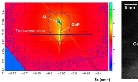
As shown in fig 7 XRD reciprocal space map (RSM) performed around the (004) GaP Bragg reflection. The alignment of both the Si(004) and GaP(004) contributions along the Sz direction, component of the diffraction vector perpendicular to the surface, is typical from a pseudomorphic growth of GaP onto vicinal Si surface.
-0.75 -0.7 -0.65 -0.6 -0.55 -0.5 -0.45 -0.4
Sx (nm-1)
Fig. 7 RSM (Synchrotron XRD ,log10 intensity levels) around
the (0 0 4) showing both the Si and the GaP contributions. The arrow shows the transverse scan path.
Fig. 8 HRTEM micrograph shows a coherent GaP/Si interface. An interfacial dislocation is identified (ED in the
image).
The coherent growth of the GaP onto silicon has been confirmed by high resolution transmission electron microscopy (HRTEM) image. The GaP/Si interface is shown to be coherent with however an interfacial dislocation (named ED in figure 8) on the right of the image. A large step bunching is also observed with a height difference of about 4nm which is much higher than the targeted 2 Si monolayer step height, suitable for avoiding APB formation. This huge step bunching has been attributed to an unoptimized chemical and thermal preparation of the surface with the presence of impurities.
4.3 Antiphase boundaries analyses
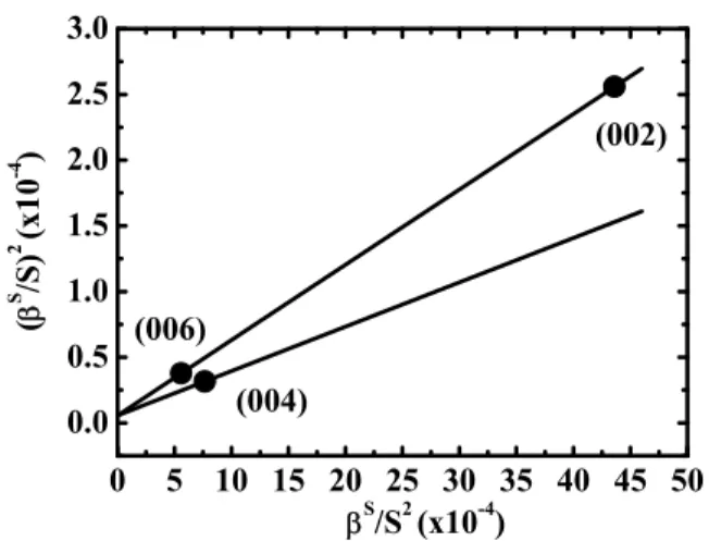
Rough information on APB density has been performed using XRD transverse scans on the (002), (004) and (006) GaP Bragg reflections, extracted from the RSM. Indeed, Ga and P scatter in antiphase around weak (002) and (006) reflections and in phase around strong (004) reflections (SR). Ga and P positions are just exchanged on both sides of an APB so that the crystal structure of each adjoining domain bounded by an APB is equivalent.27 The APB doesn’t break the lateral long range order given by epitaxy but the Antiphase
Domains (APD) gives a broad peak around antiphase reflections with a weaker peak maximum intensity, so that weak “antiphase” reflections (APR) act as APB sensors. Then, mean correlation length of defects has been determined by means of Williamson-Hall-Like (WHL) plots [38]. Weak (002) and (006) Bragg reflections give correlation length of defects including APB while strong (004) Bragg reflection gives correlation length of defects without the APB contribution [39;40].For example, WHL analyses has been applied to a sample elaborated at 350°C.The WHL plot is shown in fig.9 and gives 11 ± 1 nm for the APB correlation length along the [1 1 0] direction, while the lateral correlation length due to the other structural defects has been determined equal to 9.5 ± 1.0 nm [29].
In the same paper, RSM taken around (200), (020), (-222) and (-2-22) in grazing incidence mode, showed that these broad contributions are streaky along [110] and [1-10] directions, suggesting the presence of APD emerging at the GaP surface, with (110) and (1-10) boundaries. (200) and (020) also reveal a larger APB density along [110] direction.
0 5 10 15 20 25 30 35 40 45 50 0.0 0.5 1.0 1.5 2.0 2.5 3.0 (002) (006) (004) ( β S /S ) 2 (x1 0 -4 ) βS/S2 (x10-4)
Fig.9: WHL plots extracted from X-ray diffraction ω “transverse” scans over a GaP (00l) reflections
Fig. 10: Plan view TEM (-2 0 0) dark field of 20nmGaP/Si (S350) highlights APB.
Presence of a high APDs density has been confirmed through TEM images. Fig.10 shows a plan view of a dark field image obtained selecting the (-2 0 0) reflection. The high number of dark lines reveals a high density of APDs in this sample grown at too low temperature. The distances between APDs are also comparable to correlation lengths extracted using labsetup and synchrotron XRD.
4.4 Twin boundaries analyses
Fig. 11: Cross sectional TEM (1 1 1) dark field image of a GaAsP MQW/GaP/Si highlights planar defects in the (1 1 1) planes (TB) and also APD. Many defects reach the active area.
Numerous MTs are also present in the 20 nm-thin GaP/Si samples, as shown in the cross-section TEM image (fig.11). In order to get rid of them, we have varied the growth temperature (Tg) and performed synchrotron XRD RSMs, using a large area detector, were taken around the GaP (002) Bragg reflection.. In fig.12, the
oblique streaks under the GaP (002) Bragg reflection are characteristics of the presence of micro-twins. Four different Tg have been tested: 350°C, 400°C, 450°C, and 580°C. Preliminary results show a reduction of the TB density when increasing Tg, as confirmed by TEM observations. In a more general way, both XRD and TEM techniques show a strong reduction of planar defects densities (APBs and TBs) with the increase of Tg. However, this better quality of material is accompanied by an important increase of the roughness (characterized on TEM cross-sections). The combination of XRD and TEM was essential to characterize the defects both from a quantitative and qualitative point of view. Detailed analyses of the influence of Tg on the planar defects density will be published in a forthcoming paper.
Fig.12: Reciprocal space mapping (Synchrotron XRD) around the (002) reflection on GaP/Si samples grown at a) 400°C and b) 580°C, showing the reduction of the oblique streaks from the micro-twins with the increase of the growth temperature.
4.5 Conclusion
The quality of the GaP layers is still limited by the quality of the Si surface before the epitaxy. Work is in progress to improve the quality of that Si surface. Nevertheless, we show that the growth temperature of the GaP has a strong effect on the densities of defects as well as on the layer roughness: increasing the growth temperature lowers the defect density and increases the roughness of the sample surface.
Studies of different prelayers prior to grow the GaP buffer layer and studies of the silicon substrate misorientation influence on the GaP growth are on progress in order to improve the GaP-Si interface structural quality, and will be published in forthcoming papers.
5. TOWARD LARGER WAVELENGTH EMISSION
We have calculated the optical properties of a single monolayer InAsN inserted at midwell of 9 monolayers of GaAs alternated with a GaP barrier of 30 monolayers wide. Electronic band structure calculations are performed within the extended basis sp3d5s* tight-binding model [41]. This method provides the electronic band structure over the whole Brillouin zone, the spatial and orbital compositions of the states, and the matrix elements of optical transitions. As evidenced by our simulation (Fig 13) and in agreement with experiment, the unperturbed GaAs/GaP quantum wells grown on GaP (001) displays an X-like conduction band minimum, giving a low optical activity (the valence band maximum is an Γ-like state). A way to circumvent the type-II in k-space, is to consider an insertion of an In-like monolayer in the GaAs well which is known to act as an attractive potential for electrons [42]. This is confirmed in our simulations for an InAsN alloy with a content of nitrogen of 5% as seen in Fig 13: the conduction band minimum clearly derives from the Γ-valley localized in the surrounding of the potential perturbation. In this case, the fundamental transition is found around 1.7 eV and further engineering of the electronic structure can be performed by considering different
a)
b)
GaAs GaP 10 20 30 40 50 60 70
Atomic position
InAsN GaP hh1(r) e1(r) e1(X,y) 10 20 30 40 50 60 70Atomic position
well thicknesses and contents in order to address lower energy transitions, suitable for the chip-to-chip and within-a-chip optical interconnects and the optical telecom segments.
Fig.13: Calculated hole and electron-state wave functions of (left) a 9 ML-nm thick GaAs/GaP quantum well, and (right) including a InAsN ML inserted at mid-well inside the 9 ML-nm thick GaAs/GaP quantum well.
6. GAASPN MATERIAL FOR MULTIJUNCTION SOLAR CELLS
To date, monocristalline multi-junction solar cell devices reach the highest efficiencies conversion. Recently, the use of III-V triple junction concentrated PVs using a 1 eV diluted nitride junction has shown very promising properties, with a 44 % efficiency under 947 suns on GaAs substrate, for space applications (AM0 spectra) [43]. Concerning terrestrial applications, Spire Semiconductors has pushed solar cell record to 42.3% (AM1.5D) in 2010 with a metamorphic (lattice-mismatched) GaInP/GaAs/GaInAs triple junction under solar concentration of 406 suns, and using a lightly-doped n-type GaAs wafer. However, maintaining the GaAs, or Ge, substrates to build these high efficiency III-V solar cells, undoubtedly incurs a substantial cost associated with the substrate cost. To realise the strategic challenge of cost of 0.25-0.5 Euro/Wp, one needs to utilise a low cost, large diameter substrate from a material which is abundantly available on earth, for example silicon. For instance, a tandem solar cell, made of a 1.7 eV III-N-V top and a 1.1 eV c-Si bottom cell, would theoretically reach an efficiency of 37%, under an AM 1.5G [44]. However, efficiency of multi-junction solar cell is very sensitive to the materials quality and especially to misfit dislocations during metamorphic growth, which play an important role in the carrier lifetime (and thus reducing the current extraction), and in the solar cell lifetime. In this regard, a perfect lattice-matched epitaxial PV structure on silicon, would allow increasing significantly the efficiency, as well as reducing the overall cost of the PV multi-junction cell. The National Renewable Energy Laboratory (NREL) has demonstrated a MOCVD-grown tandem (two-junction) solar cell on a Si substrate based on GaNxP1-x-yAsy, The lattice matched n-i-p solar cell consisted of a GaP0.98N0.02:Se/GaAsPN: 1.8eV/GaP0.98N0.02:Zn top Cell and a 1.1eV diffused Si bottom cell, with a GaP
tunnel junction [45]. The growth was on Si substrates with a miscut of 2° from the (001) orientation towards (111). Though the dilute III-V nitride addresses the lattice mismatch, the efficiency achieved was about 5.2% under AM 1.5G [46] (without an anti-reflection coating), far from the theoretical maximum [45]. This low
300 nm GaP (p = 5.1018) 2.7 nm GaAsPN 30 nm GaPN (i) 300 nm GaP (n = 5.1018) GaP (n = 7.1017) Contact n
I
*5efficiency was possibly due to intrinsic defects in the GaAsPN or in the GaP/Si interface, inducing a low quantum efficiency leading to a limited current delivered by the top cell.
To reap the full benefit of the lattice matched III-V diluted nitride material systems, greater attention needs to be paid to strain and dislocation and extended defects management, unintentional impurity incorporation and nitrogen-related point defects. Growing a defect-free GaP/Si interface would thus allow to consider high efficiency lattice-matched tandem solar cells on silicon, the main issue being to find a 1.7 eV III-V absorbing layer. Most of the GaP-based materials usually absorb light higher than 1.9 eV. However, using diluted nitrides compound allows benefiting from the giant bandgap bowing due to nitrogen electronegativity.
6.1 Preliminary result on a (GaAsPN/GaPN) MQWs diode grown on GaP(001)
A (GaAsPN /GaPN) MQWs diode has been grown on a n-type GaP(100) substrate. Its structure described fig14 consists in a highly n-doped (Si doped, Nd = 5.1018 cm-3) GaP bottom layer, then a 5 QWs (2.7 nm GaAsPN/ 30 nm GaPN) and a highly p-doped (Be doped, Na = 5.1018 cm-3) GaP cap layer. The contact on the
front and back surfaces are made of annealed Ni/Au/AuZn and Ni/Au/Ge alloys respectively. The front contact is annular with a diameter of 300 µm and a width of 20 µm. Fig 15 shows the I-V characteristic of the diode under an AM1.5G illumination. The efficiency of this diode is 1.6 %, which is an encouraging result taking into account that its structure (that is, both thickness and composition of the absorbing materials, layer doping, contacts) have not been optimized, so far.
In order to optimize the crystalline quality and the absorption energy of our material bulk alloys bandgap energies have been calculated by atomic sp3d5s*sN tight-binding simulation taking into account the
description of nitrogen incorporation in a diluted regimes [47;48], and the critical thicknesses of this materials has been simulated for a range of different As and nitrogen compositions.
Fig.14: Structure of the (GaAsPN /GaPN) MQWs diode grown on GaP(001) for Solar cell applications.
-0,4 -0,2 0,0 0,2 0,4 0,6 0,8 1,0 1,2 1,4 1,6 -0,004 -0,003 -0,002 -0,001 0,000 0,001 0,002 0,003 0,004 Curr ent d ensity (A /cm²) Voltage (V)
Fig.15: Illuminated I(V) curve obtained on the (GaAsPN/GaPN) MQWs diode grown on GaP(001) without
any concentration.
6.5 (i.l I 5. 5 5.0 4.5 4.0 3.5 3.0 2.5 2.0 I I 2.0 2 4 6 8 10 12 14 16 18 As content % 1.9 1.8 Á 1.7 1.6 %As 6.2 Theoretical composition of a GaAsPN absorber lattice-matched to Si.
The bandgaps of GaAsPN are obtained using sp3s*sN tight-binging calculations adapted for the description of
nitrogen incorporation in a diluted regime [47;48]. In Fig. 16, the solid black line represents the nitrogen composition to get the lattice-matched quaternary alloys, as a function of As content. Red dotted line gives the calculated bandgap of the corresponding alloy. As an example, the GaAsPN alloy with an As content equal to 18% would need 6% of N to be lattice matched with Si, giving an alloy with an energy bandgap of 1.58 eV. From these calculations, to guarantee a 1.7 eV bandgap energy, the optimized composition of lattice-matched GaAsxPyN(1-x-y) is GaAs0.122P0.83N0.048, as it can be observed in Fig. 16 by following the black dotted line.
Fig.16: Black line represents the evolution of nitrogen content in GaAsPN alloys as a function of As giving the exact lattice
matching. Red line gives the bandgap energy for the corresponding GaAsPN alloys, as determined with sp3d5s*sN
tight binding calculations.
Fig.17: iso-contour plot of the critical thickness for GaAsPN alloy between 100 and 1000 nm
However, diluted nitride layers with high N content are known to present poor structural quality due to the large miscibility gaps between GaP and GaN [49]. Therefore, deviation from the perfect lattice-matching condition has been studied in order to lower the nitrogen incorporation. However, the goal is to keep the grown layers under the critical thickness to achieve a pseudomorphic growth. This would allow increasing the incorporation of As and reaching the expected 1.7 eV bandgap while minimizing the amount of incorporated nitrogen, as shown in the following.
6.3 Critical thickness of a GaAsPN absorber lattice-matched to Si.
Considering that a typical thickness of III-V layers grown in multijunction solar cells is around 4 µm, this value will be considered in the following as a lower limit for the critical thickness. The critical thickness of those materials is then determined using the following relationship [50;51].
(1)
Where f is the lattice mismatch with the silicon substrate, a the lattice parameter of the thin layer, b the intensity of the burgers vector, ν is the Poisson ratio of the thin layer and h the critical thickness. This model is known to be in good agreement with experimental data [52]. The validity of the Vegard’s law is assumed to be valid for these alloys [53]. The iso-contour plots of the critical thickness for GaAsPN between 100 nm and 4 µm is represented in Fig. 17, as a function of nitrogen and As content.
The value found for the GaP/Si critical thickness (absence of N and As) is equal to 90 nm. This is coherent with the experimental observations [32;54]. For the GaAsPN alloy, assuming a 4 µm threshold on critical thickness, and a maximum of 4 % nitrogen (allowing to keep reasonable crystalline quality), the As content is equal to 12%. According to tight-binding calculations, this would give a 1.76 eV bandgap for the GaAs0.12P0.84N0.04 alloy, which is close to the expected 1.7 eV energy bandgap. Therefore, a targeted 4
μm-thick absorber 1.7eV-1.8 eV bandgap GaAsPN layer can be easily grown on silicon substrate, in a pseudomorphic way, according to the critical thickness calculation.
6.4 Conclusion
First result on a diluted nitride MQWs solar cell on GaP shows promising result considering its unoptimized structure, so far. Tight binding calculation crossed with critical thickness modelling indicates that a GaAsPN alloy with a composition 12% of As and 4% of N is promising due to his expected bandgap energy (1.76 eV) and its critical thickness which allow the pseudomorphic growth of a 4 μm-thick absorber.
7. CONCLUSION
In conclusion, studies of nanostructures, either QWs or QDs, have been reported, demonstrating the suitability of the (In,Ga)As/GaP QDs system and the GaAsP(N)/GaP(N) MQWs system epitaxially grown onto GaP substrate and/or GaP/Si pseudo-substrates for laser applications. Indeed, the (In,Ga)As/GaP QDs system shows efficient RT luminescence properties, around 1.8 eV. However, the presence of two transitions at room temperature and above, likely an indirect-type ground transition followed by a direct-type second one, has to be clarified. Possible routes were also proposed in order to address lower wavelength transition and to overcome bandlineups issues, growing larger dots, or incorporating higher In content, or adding some nitride in a diluted regime inside the dots. Moreover, GaAsP(N)/GaP(N) diluted-nitride QWs-based LEDs epitaxially grown onto GaP(001) substrates have shown efficient RT EL properties at 1.7 eV, while time-resolved PL performed onto the same MQWs structure deposited onto Si, has revealed an optical limitation due to the presence of defects at the non-optimised GaP/Si interface. This prevents, so far, any obtaining of long-term stable devices. Then, thorough analyses of the GaP/Si interface using XRD, TEM and STM measurements have revealed the presence of extended defects, that are APBs and TBs. The obtained good optical properties in the aforementioned QWs system, while containing extended defects, demonstrated the room of improvement in such a diluted-nitride system. Preliminary results of the influence of the growth condition variations show a strong reduction of planar defects densities (APBs and TBs) with the increase of temperature growth. Moreover, studies of different prelayers prior to grow the GaP buffer layer and studies of the silicon substrate misorientation influence on the GaP growth are on progress and will be published in forthcoming papers.
Finally, first result on a diluted nitride MQWs solar cell on GaP substrate shows promising result with an efficiency of 2.82 % under an AM1.5G illumination. In order to optimise the solar cell structure, with the objective to obtain a tandem-cell solar cell coherently grown on a Si bottom cell, calculations have been performed to obtain a 1-μm-thick absorber at 1.7-1.8 eV, from the GaAsPN alloy. The optimal composition was found equal to 12% of As and 4% of N, taking into account the critical thickness which allow the pseudomorphic growth of this 4 μm-thick absorber.
Acknowledgments: A.Létoublon thanks V. Demange and M. Pasturel of Sciences Chimiques de Rennes for providing beam time and help on their XRD instruments.
This work is supported by the French national projects SINPHONIC (grant N°. 2011 JS03 006-01) and MENHIRS (grant N°. ANR-2011-PRGE-007-01).
REFERENCES [1] G. T. Reed, Nature 427, 595 (2004)
[2] D. A. B. Miller, Proc. IEEE 97, 1166 (2009)
[3] M. J. R. Heck, H.-W. Chen, A. W. Fang, B. R. Koch, D. Liang, H. Park, M. N. Sysak, J. E. Bowers, IEEE J. Sel. Top. Quant. Electron. 17, 333 (2011)
[4] D. Liang and J.E. Bowers, Nat Photon 4, 511 (2010)
[5] T. Egawa, Y. Murata, T. Jimbo, M. Umeno, Photonics Technology Letters, IEEE 9, 872 (1997).
[6] A. Létoublon, W. Guo, C. Cornet, A. Boulle, M. Véron, A. Bondi, O. Durand, T. Rohel, O. Dehaese, N. Chevalier, N. Bertru, A. Le Corre, J. Cryst. Growth 323, 409 (2011).
[7] K. Volz, A. Beyer, W. Witte, J. Ohlmann, I. Németh, B. Kunert, W. Stolz, Journal of Crystal Growth 315, 37 (2011).
[8] K. Momose, H. Yonezu, Y. Fujimoto, Y. Furukawa, Y. Motomura, K. Aiki, Appl. Phys. Lett. 79 , 4151 (2001).
[9] W. Guo, A. Bondi, C. Cornet, A. Létoublon, O. Durand, T. Rohel, S. Boyer-Richard, N. Bertru, S. Loualiche, J. Even, A. Le Corre, Appl. Surf. Science 258, 2808 (2012).
[10] K. Tg, K. Noguchi, S. Tanaka, Y. Furukawa, H. Okada, H. Yonezu, and A. Wakahara, Appl. Phys. Express 3, 074201 (2010)
[1
1
] B. Kunert, S.Zinnkann, K.Volz, W.Stolz
, J. Cryst. Growth 310,
4776 (2008) [12].F. Geisz and D.J. Friedman, Semicond. Sci. Technol. 17, 769 (2002).[13] N.N. Ledentsov, M. Grundmann, F. Heinrichsdorff, D. Bimberg, V.M. Ustinov, A.E. Zhukov, M.V. Maximov, Z.I. Alferov, and J.A. Lott, IEEE Journal of Selected Topics in Quantum Electronics 6, 439 (2000). [14] R. Leon, C. Lobo, T.P. Chin, J.M. Woodall, S. Fafard, S. Ruvimov, Z. Liliental-Weber, and M.A.
Stevens Kalceff, Appl. Phys. Lett. 72, 1356 (1998).
[15] W. Guo, A. Bondi, C. Cornet, H. Folliot, A. Létoublon, S. Boyer-Richard, N. Chevalier, M. Gicquel, B. Alsahwa, A.L. Corre, J. Even, O. Durand, and S. Loualiche, Phys. Status Solidi (c) 6, 2207 (2009).
[16] T.S. Shamirzaev, D.S. Abramkin, A.K. Gutakovskii, and M.A. Putyato, Appl. Phys. Lett. 97, 023108 (2010).
[17] S. Fuchi, Y. Nonogaki, H. Moriya, A. Koizumi, Y. Fujiwara, and Y. Takeda, Physica E: Low-dimensional Systems and Nanostructures 21, 36 (2004).
[18] K. Rivoire, S. Buckley, Y. Song, M.L. Lee, and J. Vučković, Phys. Rev. B 85, 045319 (2012) [19] T. Nguyen Thanh, C. Robert, C. Cornet, M. Perrin, J.M. Jancu, N. Bertru, J. Even, N. Chevalier, H. Folliot, O. Durand, and A. Le Corre, Appl. Phys. Lett. 99, 143123 (2011).
[20] C. Robert, C. Cornet, P. Turban, T. Nguyen Thanh, M. O. Nestoklon, J. Even, J. M. Jancu, M. Perrin, H. Folliot, T. Rohel, S. Tricot, A. Balocchi, D. Lagarde, X. Marie, N. Bertru, O. Durand, and A. Le Corre, Phys.Rev B 86, 205316 (2012)
[21] A.A. Mbaye, F. Turco, and J. Massies, Phys. Rev. B 37, 10419 (1988).
[22] J. Massies, F. Turco, A. Saletes, and J.P. Contour, J. Cryst. Growth 80, 307 (1987) [23] Y. Iimura, K. Nagata, Y. Aoyagi, and S. Namba, J. Cryst. Growth 105, 230 (1990).
[24] C. Cornet, C. Labbé, H. Folliot, P. Caroff, C. Levallois, O. Dehaese, J. Even, A. Le Corre, and S. Loualiche, Appl. Phys. Lett. 88, 171502 (2006)
[25] F. Fukami, K. Umeno, Y. Furukawa, N. Urakami, S. Mitsuyoshi, H. Okada, H. Yonezu, and A. Wakahara, Phys. Status Solidi (c) 8, 322 (2011).
[26] K. Umeno, Y. Furukawa, N. Urakami, R. Noma, S. Mitsuyoshi, A. Wakahara, and H. Yonezu, Physica E: Low-dimensional Systems and Nanostructures 42, 2772 (2010).
[27] C. Robert, A. Bondi, T. Nguyen Thanh, J. Even, C. Cornet, O. Durand, J.P. Burin, J.M. Jancu, W. Guo, A. Létoublon, H. Folliot, S. Boyer, M. Perrin, N. Chevalier, O. Dehaese, K. Tavernier, S. Loualiche and A. Le Corre, Appl. Phys. Lett. 98, 251110 (2011).
[28] Nguyen Thanh T., Robert C., Cornet C., Guo W., Létoublon A., Perrin M., Bertru N., Even J., Chevalier N., Folliot H., Loualiche S., Ponchet A., Elias G., Micha J.-S., Durand O., Le Corre A., Photonics west 2012 San Francisco (2012-01-21) IEEE, Proceedings of the SPIE, Vol. 8268, 82681H.
[29] T. Nguyen Thanh, C. Robert, W. Guo, A. Létoublon C. Cornet, G. Elias, A. Ponchet, T. Rohel, N. Bertru, A. Ballochi, O. Durand, J.S. Micha, M. Perrin, S. Loualiche, X. Marie and A. Le Corre, J. Appl. Phys, 112, 053521 (2012)
[30] A. Erol, editor, Dilute III-V Nitride Semiconductors and Material Systems: Physics and Technology, 1st ed. (Springer, 2008).
[31] S.F. Fang, K. Adomi, S. Iyer, H. Morkoç, H. Zabel, C. Choi, and N. Otsuka, J. Appl. Phys. 68, R31 (1990).
[32] O. Skibitzki, F. Hatami, Y. Yamamoto, P. Zaumseil, A. Trampert, M.A. Schubert, B. Tillack, W.T. Masselink, and T. Schroeder, J. Appl. Phys. 111, 073515 (2012).
[33] R.J. Potter and N. Balkan, Journal of Physics: Condensed Matter 16, S3387 (2004).
[34] Y. Takagi, H. Yonezu, K. Samonji, T. Tsuji, and N. Ohshima, J. Cryst. Growth 187, 42 (1998). [35] H. Kroemer, J. Cryst. Growth 81, 193 (1987).
[36] R.M. Sieg, S.A. Ringel, S.M. Ting, E.A. Fitzgerald, and R.N. Sacks, J. Electron. Mater. 27, 900 (1998). [37] J.-F. Berar, N. Boudet, P. Breugnon, B. Caillot, B. Chantepie, J.-C. Clemens, P. Delpierre, B.
Dinkespiller, S. Godiot, C. Meessen, M. Menouni, C. Morel, P. Pangaud, E. Vigeolas, S. Hustache, K. Medjoubi, Nuclear Instruments and Methods in Physics Research Section A: Accelerators, Spectrometers, Detectors and Associated Equipment 607, 233 (2009)
[38] O. Durand, A. Letoublon, D.J. Rogers, and F. Hosseini Teherani, Thin Solid Films 519, 6369 (2011). [39] O. Durand, A. Letoublon, D.J. Rogers, F.H. Teherani, C. Cornet, and A. Le Corre, Proc. SPIE 7940 79400L (2011).
[40] H. Jussila, S. Nagarajan, T. Huhtio, H. Lipsanen, T.O. Tuomi, and M. Sopanen, J. Appl. Phys. 111, 043518 (2012).
[41] J. M. Jancu, R. Scholz, F. Beltram, and F. Bassani Phys. Rev. B 57, 6493 (1998)
[42] R. Samti, F. Raouafi, M. Chaouach, M. Maaref, A. Sakri, J. Even, J.-M. Gerard, and J.-M Jancu, Appl. Phys. Lett. 101, 12105 (2012)
[43] Solar International, issue VIII 2012, p7, www.solar-international.net. [44] S. R. Kurtz, P. Faine, and J. M Olson, J. Appl. Phys. 68, 1890 (1990)
[45] J. Geisz et al, DOE Solar Energy Technologies, Program Review Meeting, October 25-28, 2004, Denver, Colorado
[46] J.F. Geisz et al, 31st IEEE Photovoltaics Specialists Conference and Exhibition, Lake Buena Vista,
Florida, January 3-7, 2005
[47] N. Shtinkov, P. Desjardins, and R.A. Masut, Phys. Rev. B 67, 081202 (2003).
[48] C. Robert, M. Perrin, C. Cornet, J. Even, and J.M. Jancu, Applied Physics Letters 100, 111901 (2012) [49] I. Ho and G.B. Stringfellow, Journal of Crystal Growth 178, 1 (1997)
[50] R. People and J.C. Bean, Applied Physics Letters 47, 322 (1985). [51] R. People and J.C. Bean, Applied Physics Letters 49, 229 (1986).
[52] W. Shan, W. Walukiewicz, K.M. Yu, J. Wu, J.W. Ager, E.E. Haller, H.P. Xin, and C.W. Tu, Ap-plied Physics Letters 76, 3251 (2000).
[53] L. Vegard, Zeitschrift Für Physik A Hadrons and Nuclei 5, 17 (1921)
[54] Y. Takagi, Y. Furukawa, A. Wakahara, and H. Kan, Journal of Applied Physics 107, 063506 (2010).