HAL Id: hal-00832250
https://hal.archives-ouvertes.fr/hal-00832250v2
Submitted on 3 Jan 2014
HAL is a multi-disciplinary open access archive for the deposit and dissemination of sci-entific research documents, whether they are pub-lished or not. The documents may come from teaching and research institutions in France or abroad, or from public or private research centers.
L’archive ouverte pluridisciplinaire HAL, est destinée au dépôt et à la diffusion de documents scientifiques de niveau recherche, publiés ou non, émanant des établissements d’enseignement et de recherche français ou étrangers, des laboratoires publics ou privés.
Coupling
Sjoerd Op ’T Land, Richard Perdriau, Mohamed Ramdani, Marco Leone,
M’Hamed Drissi
To cite this version:
Sjoerd Op ’T Land, Richard Perdriau, Mohamed Ramdani, Marco Leone, M’Hamed Drissi. Simple, Taylor-based Worst-case Model for Field-to-line Coupling. Progress In Electromagnetics Research, EMW Publishing, 2013, 140, pp.297-311. �10.2528/PIER13041207�. �hal-00832250v2�
SIMPLE, TAYLOR-BASED WORST-CASE MODEL FOR FIELD-TO-LINE COUPLING
Sjoerd T. Op ’t Land1, *, Mohamed Ramdani1,
Richard Perdriau1, Marco Leone2, and M’hamed Drissi3
1Groupe ESEO, EMC Research Group, 10 boulevard Jeanneteau,
49107 Angers Cedex 2, France
2Otto-von-Guericke-Universit¨at Magdeburg, Universit¨atsplatz 2,
Ma-gdeburg 39106, Germany
3Universit´e europ´eenne de Bretagne IETR, INSA de Rennes, 20 avenue
des Buttes de Co¨esmes, 35708 Rennes Cedex 7, France
Abstract—To obtain Electromagnetic Compatibility (EMC), we would like to study the worst-case electromagnetic field-induced voltages at the ends of Printed Circuit Board (PCB) traces. With increasing frequencies, modelling these traces as electrically short no longer suffices. Accurate long line models exist, but are too complicated to easily induce the worst case. Therefore, we need a simple analytical model. In this article, we predict the terminal voltages of an electrically long, two-wire transmission line with characteristic loads in vacuum, excited by a linearly polarised plane wave. The model consists of a short line model (one Taylor cell) with an intuitive correction factor for long line effects: the modified Taylor cell. We then adapt the model to the case of a PCB trace above a ground plane, illuminated by a grazing, vertically polarised wave. For this case, we prove that end-fire illumination constitutes the worst case. We derive the worst-case envelope and try to falsify it by measurement in a Gigahertz Transverse Electromagnetic (GTEM) cell.
1. INTRODUCTION
Pursuing Electromagnetic Compatibility (EMC) is resolving unwanted electromagnetic interactions between electronic systems. The number of possible combinations and configurations of electronic systems is
Received 12 April 2013, Accepted 22 May 2013, Scheduled 4 June 2013 * Corresponding author: Sjoerd T. Op ’t Land ([email protected]).
infinite, so simplification techniques are always employed to enable analysis.
A common simplification is that of weak coupling: we choose to consider two systems an aggressor and a victim, and we only consider the effect of the electromagnetic field generated by the aggressor on the victim. Because the coupling is weak, we can neglect the resulting effect on the aggressor. This simplification allows us to speak about emission (by the aggressor) and susceptibility (of the victim). In this paradigm, EMC can be obtained by reducing emission and/or reducing susceptibility.
Another simplification is to only look at the worst case. For example, if we are sure that decreasing the distance between aggressor and victim makes things worse, it suffices to prove that there is no unwanted interaction at the smallest distance that can possibly occur. Instead of having to prove EMC for all distances, we only need to prove it for one particular distance (the worst case). As EMC depends, amongst others, on the distance, we imagine distance as a dimension of the problem space. Considering the worst case of one variable decreases the dimension of the problem space by one.
Finally, we often characterize emission and susceptibility in terms of the far field magnitude. In general, an aggressor can generate any spatiotemporal field that satisfies the Maxwell equations. Hence, it needs to be described as ~E(~r, t) or ~H(~r, t). At some distance from the aggressor, however, the field tends to a plane wave with the wave impedance of the vacuum. Assuming susceptibility to be independent of the relative phase of the field’s spectral components, we describe it with the magnitude vector of its Fourier transform: | ~E(~r, !)|. Assuming a linearly polarized wave, the field only decays with the distance ~r. Now, the vector | ~E(!)| at a rough distance suffices to describe the emissivity of a system. Reciprocally, we can describe the susceptibility of a system in terms of a maximum allowed electric field magnitude vector.
To assess the susceptibility of Printed Circuit Boards (PCBs), we would like to be able to reason analytically about the voltages induced at PCB trace terminals by an incident electromagnetic field. Particularly, we would like to dispose of tools to induce the worst case: the maximum voltage. For that reason, we look for easy-to-understand analytical expressions that show the relation with designable parameters (transparent equations).
We start by reviewing prior work on this question in Section 2, indicating the lack of transparent models for electrically long lines. A new, transparent model for two-wire transmission lines is proposed in Section 3. The model does not provide a strong upper bound to the
induced voltages. To that end, the model is specialised for grazing-incident wave on a PCB trace in Section 4. The low-frequency and high-frequency worst cases are derived and joined to give a broadband worst-case envelope. To challenge the resulting model, an experiment is performed and commented upon in Section 5. Having failed to falsify the model by measurement and by comparison with earlier work, we conclude in Section 6.
2. STATE OF THE ART
The quest for worst-case or typical-case induced voltages at the terminals of PCB traces is not new: Lagos developed a numerical algorithm to find the worst case with known load impedances [1]. Magdowski derived analytical expressions for the typical case [2], that is: for random illumination. Neither model is transparent, so we will now look for general field-to-trace models (not worst case).
A model based on Maxwell’s equations will not be weakly coupled. Moreover, closed-form and transparent solutions to Maxwell’s equations are rare. Therefore, we will need an acceptable approximation of Maxwell’s equations.
The quasi-static approximation lets waves propagate infinitely fast: c0 ! 1, which is representative for structures that are sufficiently
small with respect to the wavelength. With susceptibility tests up to 18 GHz, free-space wavelength descends to 1.7 cm, while PCB traces may be tens of centimetres in length: too simplistic.
An intermediate approximation is that of transmission line theory: the supposition that there be only a differential transverse electromagnetic mode (TEM). The common mode can be ignored, because the ground planes of modern PCBs suppress it and because the common mode response across the terminals is generally small [3, 4]. A typical microstrip line gradually becomes multimodal from some GHz upward [5], so this simplification might hold.
With coupled lines theory, Mandi´c predicted the coupling between a TEM cell septum and PCB traces [6] with a circuit simulator. His model is not transparent, nor is it weakly coupled.
There are three equivalent, weakly coupled transmission line based models [3]: that of Taylor et al. [7], Agrawal et al. [8] and that of Rachidi [9]. They all model a transmission line as a cascade of cells. As the wavelength along the line decreases, the line needs to be considered as a cascade of short enough cells, such that the field is uniform enough along each cell. From two cells upward, the terminal voltage expressions are no longer transparent.
succeeded to find transparent expressions [5]. Firstly, he assumed that both loads be matched, which he showed to be a reasonable approximation for moderately mismatched loads. Secondly, the transient excitation should be mainly low-frequency, which is reasonable for nuclear electromagnetic pulse (NEMP) testing. From his model, he concludes that end-fire (parallel with the line), vertically-polarised illumination constitutes the worst case for the near-end terminal.
For continuous wave (CW) testing, the second approximation does not necessarily hold. Furthermore, we would like to better understand why end-fire, vertically-polarised illumination is the worst case for the far end. Therefore, we set out to develop a model of our own.
3. TAYLOR-BASED TRANSPARENT MODEL
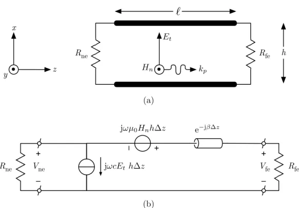
We base our transparent model on Taylor’s (Figure 1), because we like the distributed contribution of the electric and magnetic fields.
3.1. Long-line Analysis
At low frequencies, the wavelength is much greater than the line length. Therefore, the excitation field can be approximated as uniform and we can model the transmission line as a single Taylor’s cell, cf. Figure 1(b). For simplicity, we terminate the line in its characteristic impedance to avoid reflections.
We are interested in the near-end and the far-end terminal voltages Vne and Vfe. Unless otherwise noted, we will present the results
simultaneously and call them either-end. For example, the ± operator means plus for the near end and minus for the far end (vice versa for ®). By inspecting Figure 1(b) with ∆z = `, Rne = Rfe = Zc and
Ø∆z # 0, we find the low-frequency, either-end induced voltage to be VLF= °
1
2Zc j!cEt h` ® 1
2 j!µ0Hn h`, (1) where Et is the excitation E-field component transversal to the line,
Hn the excitation H-field component normal to the line, h the distance
between the wires, and ` the line’s length.
With increasing frequency, wavelengths decrease, both in free space and in transmission lines: the line becomes electrically long.
In free space, we assume a linearly polarised plane wave with wave vector k. The fields along the line are then retarded by a phasor i:
i(z) = e°jkpz (2)
Rne Rfe h Hn Et
ℓ
kp + – Rfe Rne jωcEt h∆z + – Vne Vfe + – jωµ0Hnh∆z e−jβ∆z x z y (a) (b)Figure 1: Modelling a two-wire transmission line excited by an electromagnetic wave. (a) Line geometry: subscripts t, n and p (or x, y and z) denote excitation field components transversal, normal and parallel to the line segment, respectively. Rne and Rfe are the
near-end and far-end resistive terminations. (b) Taylor’s line segment model (cell): approximation of passive transmission line segment ∆z, with a voltage source representing the electromotive force (emf) and current source representing the electrostatic force (electric induction). c denotes the per-unit-length (PUL) capacity of the line.
Hn(z) = Hn(0)i(z) = Hn(0)e°jkpz, (4)
where kp denotes the excitation wave vector’s component parallel to
the line. We will call i the normalised excitation field amplitude. As for a transmission line, the voltage along the line is the superposition of a forward- and a backward travelling eigenwave. They can both be described with a phasor w that lags or leads, respectively.
w±(z) = e±jØz (5)
V (z) = V°w+(z) + V+w°(z) = V°e+jØz + V+e°jØz, (6)
where Ø is the line’s wave number, V° the backward going wave
voltage, and V+ the forward going wave voltage. All complex amplitudes have their phase reference at z = 0: i.e., V (0) = V°+ V+.
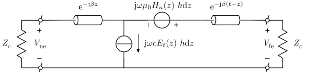
To find the terminal voltage, we integrate cells with length dz over the line’s length. The passive transmission lines at the left and right of this sliding cell have length z and ` ° z respectively (cf. Figure 2).
+ – Zc Zc + – Vne Vfe + – jωµ0Hn(z) hdz jωcEt(z) hdz e−jβz e−jβ(ℓ−z)
Figure 2: Modelling an electrically long, lossless two-wire transmission line with characteristic loads as the continuous integral of infinitesimal cells of length dz.
Both sources of the infinitesimal cell directly see a characteristic load, so (1) gives the backward- and forward traveling voltages. The near-end voltage contribution of the infinitesimal cell is then delayed by the left half z of the transmission line:
dVne = µ °1 2Zc j!cEt(z) hdz ° 1 2 j!µ0Hn(z) hdz ∂ e°jØz = 1 2j! (°ZccEt(0) ° µ0Hn(0)) e°jk pz e°jØz hdz (7) Vne = 1 2j! (°ZccEt(0) ° µ0Hn(0)) h Z ` 0 e°jkpze°jØz dz. (8)
Similarly, the far-end voltage contribution is delayed by the right half (` ° z) of the transmission line, and we obtain:
Vfe = 12j! (°ZccEt(0) + µ0Hn(0)) h
R`
0 e°jkpze+jØz dz e°jØ`. (9)
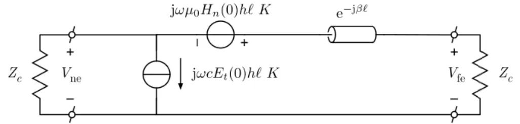
3.2. Circuit Model Interpretation
Let us now try to interpret the result as an equivalent circuit in order to develop intuition. By slightly rewriting (8) and (9), we can recognise the low-frequency induced voltage of (1), multiplied by a factor K:
K = 1 ` Z ` 0 e°jkpze®jØz dz = 1 j(kp® Ø)` ≥ ej(kp®Ø)`° 1¥, (10)
with an additional factor e°jØ` for the far end. This result is visualised
in Figure 3: a single Taylor-like cell, also valid for high frequencies. To better understand the meaning of K, consider the non-physical case where the excitation wave travels with the same phase speed along
+ – Zc Zc + – Vne Vfe + – e−jβℓ jωµ0Hn(0)hℓ K jωcEt(0)hℓ K
Figure 3: The modified Taylor cell (compare with Figure 1(b)). The correction factor |K| 6 1 takes into account the long line effect.
the line as a wave on the line: Ø = kp. By inspecting (10), one sees
that Kfar end is unity, for any frequency or line length. So it is not only
the non-uniformity of the excitation field that invalidates a single-cell Taylor model.
It is rather the discrepancy between Ø and kpthat makes K deviate
from unity. Using the normalised amplitude of the excitation wave i and of the line’s eigenwave w (cf. (2) and (5)), we can now interpret K as a length-average conjugated product:
K = 1 `
Z `
0 i(z) · w
§(z) dz, (11)
which is the length-average cross-correlation or similarity of the excitation wave and a wave that would propagate on the line.
3.3. A Strict Upper Bound
Looking at (9), we recognise that the line delay only introduces a phase shift, so it can be ignored. Both near-end and far-end voltage magnitudes are determined by the low-frequency terminal voltage VLF
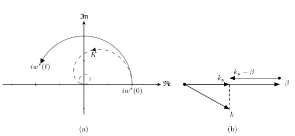
and the correction factor K. Let us first find the worst |K|, and then the worst |VLF|.
Let us interpret K geometrically on the complex plane. The integrand iw§(z) yields the similarity of the excitation plane wave and
the line’s eigenwave at each position z on the transmission line. At the beginning of the line, both have the same phase. As i and w are normalised amplitudes, the integrand amounts to one. Due to the different propagation speeds of the excitation wave and the line’s eigenwave, the phase difference grows along the line. The arc described by the integrand in the case of a forward propagating wave is shown in Figure 4.
The integral divided by its length yields the arc’s centre of gravity K. By inspecting Figure 4, we see that |K| 6 1. Moreover, the smaller the phase difference at the end of the line, the shorter the arc, the
Im K iw∗(0) iw∗(ℓ) Re β k k p k p− β (a) (b)
Figure 4: Geometric interpretations of factors contributing to K. (a) On the complex plane: K is the centre of gravity of the arc iw§(z). The trajectory of K is dashed for 0 6 iw§(`) 6 4º. (b) In Cartesian
space: wave vector alignment with the transmission line.
greater |K|. The phase difference at the end of the line is (kp° Ø)`.
Hence, for a given `, the worst case occurs when kp and Ø are closest.
Let us picture the line’s wavenumber Ø as a vector pointing in the line direction. The excitation wave vector parallel to the line kp is then
the projection of k on the first vector. Moreover, as the excitation wave always propagates faster than a wave on the line, k is always shorter than Ø, as is the case in Figure 4(b).
By inspection, we see that kp° Ø is minimal when the excitation
wave vector k is parallel with the line. Therefore, |Kfar end| is maximum
when exciting from the near-end side, parallel to the line (end-fire excitation). Physically speaking, the worst case occurs when the excitation propagates towards the studied end.
As for the worst-case VLF, E and H need to be expressed as
function of the angle of incidence and polarisation. In the case of a microstrip trace, the incident wave is refracted by the air-dielectric interface and then reflected by the ground plane, which is not simple. Leone showed that the worst case occurs under end-fire excitation, when the excitation propagated away from the studied end [5]. Therefore, we cannot easily join both worst cases to obtain a broadband worst case.
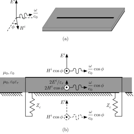
4. GRAZING INCIDENCE ON A PCB TRACE
In order to draw a broadband worst-case conclusion, we will specialise the model for a simple and practical case. As will be shown, the fields
µ0, ε0 µ0, ε0εr Ei Zc Zc 2Hicosφ 2Ei/εr ω c0 cosφ φ ω c0 Ei ω c0 cosφ Ei ω c0 cosφ Hicosφ Hi Hicosφ (a) (b)
Figure 5: Approximation of the substrate field strength for grazing incidence. (a) Perspective on the grazing incident wave: the incident electric field is perpendicular to the substrate and the wave vector makes an angle ¡ with the transmission line axis. (b) Cross section of the transmission line. The incident and reflected plane wave sources produce the shown substrate field.
remain simple in the case of grazing incidence (see Figure 5(a)). This case is also practical, because PCBs in a GTEM cell wall are subjected to a grazing incident field.
4.1. Substrate Fields
A PCB trace differs from a two-wire transmission line: it contains a ground plane and a dielectric layer.
As for the ground plane: it acts as a mirror to the far-field incident source [4]. Therefore, there is no field below the ground plane and the field above the ground plane is doubled in the case of grazing incidence. If the dielectric substrate is relatively thin, the incident grazing wave will not be slowed down by the dielectric (cf. µ ! º2 in [5]).
with a constant phase lag: k = ki = !/c
0 and kp = cos(¡) !/c0. For
dielectric substrates, there is no difference in permeability, so H = 2Hi
and Hn = cos(¡) 2Hi. However, because of the different permittivity,
the electric field will be weaker: Et = 2Ei/"r (cf. (30) of [5]). The
resulting substrate field is visualised in Figure 5(b). 4.2. Low-frequency Worst Case
We can now express the low-frequency terminal voltage under grazing incidence in terms of Ei and ¡:
Zc = 1 cvline = p"r,eff c c0 ; E i = Hir µ0 "0; c0 = 1 pµ 0"0 VLF = 1 2j! µ °Zcc 2Ei "r ® µ0 2Hicos(¡) ∂ h` = jkiEi µ °p"r,eff "r ® cos(¡) ∂ h`. (12)
By inspecting (12), we see that the worst-case near-end (far-end) induced voltage occurs for ¡ = 0 (¡ = º), consistent with [5].
4.3. High-frequency Worst Case
Let us now find the worst-case ¡ for a given Ei, h, `, "r and "r,eff.
K = 1 j(°kicos(¡) ® Ø)` ≥ ej(°kicos(¡)®Ø)`° 1¥, (13) |V |=|VLF||K|=Eih Ø Ø Ø Ø Ø °p"r,eff "r ® cos(¡) ° cos(¡) ® p"r,eff Ø Ø Ø Ø Ø Ø Ø Øe j!(° cos(¡)®p"r,eff)c0` °1ØØ Ø. (14) The rightmost term determines the worst case frequency, then amounting to 2. The rest is frequency and length (!) independent.
Knowing that p"r,eff > 1 and for given Ei, h, "r and "r,eff,
max !` |V | = 2E ih Ø Ø Ø Ø° p"r,eff "r ®cos(¡) Ø Ø Ø Ø p" r,eff±cos(¡) . (15)
In order to find the maximum with respect to ¡, we would like to differentiate and equate to zero to find the critical points. However, for ¡ where the enumerator sign flips over, the fraction is not differentiable. Fortunately, these ¡ constitute the minima, whereas we search the maxima. We ignore the absolute operator (critical points stay critical):
@ @¡max!` |V | = 2E ih®p"r,eff ≥ 1 ° "1r ¥ sin(¡) °p" r,eff± cos(¡)¢2 . (16)
The denominator is never zero, so the derivative only equals zero for ¡ = 0, º: we only need to consider end-fire illumination.
Let us compare ¡ = 0 (left hand side) and ¡ = º (right hand side) for the near-end case of (15) (recall that p"r,eff < "r,eff < "r):
1 + p"r,eff "r p"r,eff+ 1 7 1 ° p" r,eff "r p"r,eff° 1 ) "r,eff "r ° 1 7 1 ° "r,eff "r , (17) so ¡ = º constitutes the worst case for the near end.
By plugging these worst-case ¡ into (15), we conclude: max !`,¡|V | = 2E ih1 ° p" r,eff "r p"r,eff° 1 , (18)
which is the high-frequency, worst-case, either-end induced voltage in a characteristically terminated microstrip illuminated under grazing incidence.
4.4. Broadband Worst Case
We propose to join (12) and (18) to obtain a broadband worst case:
max |V | = Eih · min ( ! c0` µ 1 + p"r,eff "r ∂ , 21 ° p" r,eff "r p"r,eff° 1 ) , (19)
magnetic electric magnetic electric
that is, the envelope formed by the low-frequency near-end voltage for ¡ = 0 and the high-frequency voltage for ¡ = º.
This can be physically interpreted as follows: for low frequencies, the worst case occurs when the magnetic and the electric contributions add up constructively. The wavelength is great with respect to the line length, so the line does not feel the difference between a forward or a backward travelling wave: Kfar end = Knear end = 1.
For high frequencies, the worst case occurs when the illuminating wave is aligned with the wave propagating towards the terminal. The magnetic and electric contributions cancel somewhat, but the alignment (K ! 1) has a bigger effect.
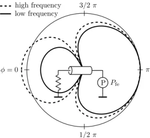
The antenna pattern of Figure 6 illustrates the response of the far end. Notice the deep null, which occurs at
cos(¡) = ®p"r,eff "r
, (20)
P Pfe φ = 0 1/2 π π 3/2 π high frequency low frequency
Figure 6: Qualitative antenna pattern of the far end. The radial axis has no particular unit: the low-frequency gain of (12) is linear in !, the high-frequency gain of (15) is normalised to coincide with the low-frequency gain at ¡ = º.
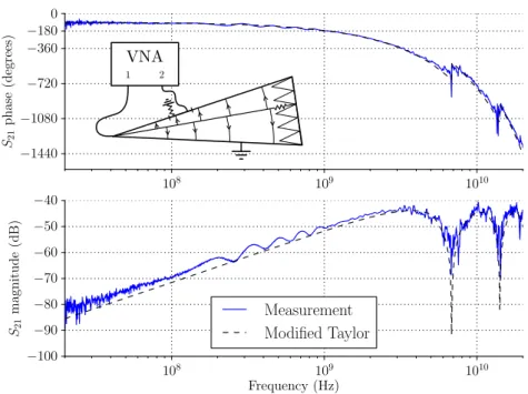
5. EXPERIMENT
We now design and perform an experiment that challenges the model: do the simplifying assumptions hold in a practical case?
A practical plane wave source is the GTEM-cell: a tapered rectangular waveguide with a metallic strip as centre conductor, the septum. Our Teseq GTEM 250A-SAE sports a square top wall opening to illuminate a PCB. The approximate field strength 2Ei over the PCB is found by dividing the septum voltage by the average septum distance (dseptum = 42.2 mm) [10].
We create a suitable PCB in an industrial, four-layer FR4 process. On the top layer, we draw a 5 cm, 50 Ω microstrip with respect to the ground layers below. At the bottom, precision SMA connectors allow for connection to the far end and the near end.
We choose to measure the far-end voltage. To quantify the induced voltage for a known septum voltage, we use a two-port Vector Network Analyser (VNA), an Agilent N5247A. We connect its first port to the GTEM-cell’s input, and the second port to the trace’s far end. We terminate the near end with a broadband 50 Ω load. As both the input of the GTEM cell and the VNA have 50 Ω impedance, the S21
also equals the voltage transfer from the septum to the far end. The S21 can therefore be predicted with (14), with 2Ei = 1/dseptum, cf.
Figure 7.
The log-frequency average difference between prediction and measurement is °1.9 dB over the 20 MHz to 20 GHz, range. The
108 109 1010 −1440 −1080 −720 −360 −180 0 S21 phase (degrees) 108 109 1010 Frequency (Hz) −100 −90 −80 −70 −60 −50 −40 S21 magnitude (dB) Measurement Modified Taylor VNA 1 2
Figure 7: Calculated and measured S21 of the microstrip trace,
illuminated in a GTEM cell. Port 1 is the GTEM cell input, port 2 is the trace’s far end, while the near end is terminated in 50 Ω.
average absolute deviation from this bias is 1.4 dB. We repeated the measurement and prediction in all PCB orientations (¡ = 0, 12º, º, 32º), measuring both near-end and far-end coupling: 8 cases in all. We obtained similar agreement: an average error of °1.8 dB and an average absolute deviation of 1.8 dB. Four far-end measurements are compared with the worst-case envelope of (19) in Figure 8.
108 109 1010 Frequency (Hz) −90 −80 −70 −60 −50 −40 −30 −20 S21 magnitude (dB) Endfire far-end Endfire near-end Broadside far-end Broadside near-end Upper bound |V |= ω c0 Ei ! 1 + √ εr,eff εr " hℓ |V | = 2Eih1 − √εr,eff εr √ε r,eff− 1
Figure 8: Measured either-end coupling with the PCB in two different orientations and the analytical upper bound ((19)). The high-frequency asymptote is not flat because "r(f ) was measured and taken
In an attempt to explain the discrepancies, we assess the electric field homogeneity by measuring the transfer to an uncalibrated E-field sensor. We measured the transfer at four different positions and compared the transfers. Up to 5 GHz, the log-frequency averaged difference between the maximum and minimum transfer is 1.4 dB and between 5–20 GHz it is 5.8 dB. These numbers give an idea of the field homogeneity in the GTEM cel.
6. CONCLUSIONS
Using Taylor’s field-to-line coupling model, we calculated the high-frequency coupling to a characteristically-terminated two-wire transmission line in vacuum. We formulated the result as the product of the low-frequency coupling and a correction factor K. We gave geometrical interpretations of the correction factor that allow to reason about the worst case.
The coupling of a plane wave incident on a PCB trace above a ground plane is harder to calculate because of the reflected wave. Therefore, we limited ourselves to the case of grazing incidence: a wave polarisation perpendicular to the PCB surface. For this problem class, we found the worst-case induced terminal voltage. For low frequencies, the worst case occurs for end-fire excitation at the illuminated end. For high frequencies, the worst case still occurs for end-fire excitation, but at the opposite end. By joining both asymptotes, we provided a transparent broadband worst-case envelope.
The low-frequency solution (12) equals (49) of [5] for the case of grazing incidence (i.e., by filling in µ = 12º and ∞ = 0). Measurements on a microstrip trace in a GTEM cell did not falsify the broadband envelope, either.
Collaterally, we noticed a broadband deep null in the antenna pattern of a microstrip trace. This reveals a weakness of PCB testing with a GTEM cell: there may be blind angles.
ACKNOWLEDGMENT
This bit of research was made possible by the French national project SEISME (simulation of emissions and immunity of electronic systems). Marianne de Wolf at Eurocircuits patiently taught us some photolithographical fabrication constraints. Damien Guitton, Fabien Tessier and Sylvain Perpoil of ESEO’s technical support offered their precious time to enable our measurements. Olivier Maurice showed us that fundamental and applied research are not mutually exclusive.
Finally, we are grateful for nature’s consistency; predicting its behaviour is neither easy nor impossible.
REFERENCES
1. Lagos, J. L. and F. L. Fiori, “Worst-case induced disturbances in digital and analog interchip interconnects by an external electromagnetic plane wave — Part I: Modeling and algorithm,” IEEE Transactions on Electromagnetic Compatibility, Vol. 99, 1– 7, 2010.
2. Magdowski, M. and R. Vick, “Closed-form formulas for the stochastic electromagnetic field coupling to a transmission line with arbitrary loads,” IEEE Transactions on Electromagnetic Compatibility, Vol. 99, 1–7, 2012.
3. Nucci, C. A., F. Rachidi, and M. Rubinstein, “An overview of field-to-transmission line interaction,” Applied Computational Electromagnetics Society Newsletter, Vol. 22, No. 1, 9–27, 2007. 4. Paul, C. R., Introduction to Electromagnetic Compatibility, Wiley,
2006.
5. Leone, M. and H. L. Singer, “On the coupling of an external electromagnetic field to a printed circuit board trace,” IEEE Transactions on Electromagnetic Compatibility, Vol. 41, No. 4, 418–424, Nov. 1999.
6. Mandi´c, T., R. Gillon, B. Nauwelaers, and A. Bari´c, “Character-izing the TEM cell electric and magnetic field coupling to PCB transmission lines,” IEEE Transactions on Electromagnetic Com-patibility, Vol. 54, No. 5, 976–985, Oct. 2012.
7. Taylor, C. D., R. S. Satterwhite, and C. W. Harrison, Jr., “The response of a terminated two-wire transmission line excited by a nonuniform electromagnetic field,” IEEE Transactions on Antennas and Propagation, Vol. 13, No. 6, 987–989, Nov. 1965. 8. Agrawal, A. K., H. J. Price, and S. H. Gurbaxani, “Transient
re-sponse of multiconductor transmission lines excited by a nonuni-form electromagnetic field,” IEEE Transactions on Electromag-netic Compatibility, Vol. 22, No. 2, 119–129, May 1980.
9. Rachidi, F., “Formulation of the field-to-transmission line coupling equations in terms of magnetic excitation field,” IEEE Transactions on Electromagnetic Compatibility, Vol. 35, No. 3, 404–407, Aug. 1993.
10. IEC 62132-2, “Integrated circuits — Measurement of electromag-netic immunity 150 kHz to 1 GHz — Part 2: Measurement of ra-diated immunity-TEM-cell method,” Jul. 2004.