HAL Id: tel-01082283
https://tel.archives-ouvertes.fr/tel-01082283
Submitted on 13 Nov 2014
HAL is a multi-disciplinary open access
archive for the deposit and dissemination of sci-entific research documents, whether they are pub-lished or not. The documents may come from teaching and research institutions in France or abroad, or from public or private research centers.
L’archive ouverte pluridisciplinaire HAL, est destinée au dépôt et à la diffusion de documents scientifiques de niveau recherche, publiés ou non, émanant des établissements d’enseignement et de recherche français ou étrangers, des laboratoires publics ou privés.
emission on Si
Cédric Robert
To cite this version:
Cédric Robert. Study of III-V nanostructures on GaP for lasing emission on Si. Optics / Photonic. INSA de Rennes, 2013. English. �NNT : 2013ISAR1913�. �tel-01082283�
Thèse
THESE INSA Rennes sous le sceau de l’Université européenne de Bretagne pour obtenir le titre de DOCTEUR DE L’INSA DE RENNES Spécialité : Physique-Optoélectronique présentée par
Cédric Robert
ECOLE DOCTORALE : SDLM LABORATOIRE : FOTONStudy of III-V
nanotructures on GaP
for lasing emission on Si
Thèse soutenue le 27.08.2013
devant le jury composé de : Olivier Durand
Professeur (FOTON, INSA Rennes) / Président du jury
Paul Voisin
Directeur de recherches CNRS (LPN) / Rapporteur
Yves Rouillard
Maître de conférences HDR (IES, Université Montpellier 2) / Rapporteur
Udo W. Pohl
Professor Doctor (Technische Universität Berlin) / Examinateur
Alejandro R. Goñi
Professor (CSIC-ICMAB Barcelona) / Examinateur
Marc-André Dupertuis
Maître d’enseignement et de recherche (EPFL Lausanne) / Examinateur
Jacky Even
Professeur (FOTON, INSA Rennes) / Directeur de thèse
Charles Cornet
Maître de conférences (FOTON, INSA Rennes) / Co-encadrant de thèse
Cédric ROBER
T
2013
Institut National des Sciences Appliquées de Rennes 20, Avenue des Buttes de Coësmes CS 70839 F-35708 Rennes Cedex 7 Tel : 02 23 23 82 00 - Fax : 02 23 23 83 96
N° d’ordre : 13ISAR 19 / D13-19
Ce travail de thèse porte sur l’étude de nanostructures semi-conductrices III-V pour le développement d’émetteurs laser sur silicium dans une approche pseudomorphique. Une croissance en accord de maille d’alliages à base de GaP ou plus précisément de nitrures dilués GaPN doit garantir une faible densité de défauts cristallins. Le modèle des liaisons fortes à base étendue est tout d’abord présenté afin de simuler les propriétés électroniques et optiques de structures semi-conductrices sur substrats de GaP ou Si. Les propriétés des alliages massifs GaPN et GaAsPN sont étudiées par des expériences de photoluminescence continue en fonction de la température et de photoluminescence résolue en temps. Les potentialités des puits quantiques GaAsPN/GaP en tant que zone active sont étudiées théoriquement par le modèle des liaisons fortes et expérimentalement en spectroscopie de photoluminescence en température et résolue en temps. Les effets de désordre engendrés par l’incorporation d’azote sont notamment mis en évidence. L’alliage AlGaP est ensuite proposé pour les couches de confinement optique des structures laser. Un contraste d’indice optique entre AlGaP et GaP est mesuré par ellipsométrie spectroscopique. Ce contraste doit permettre un confinement efficace du mode optique. Le problème de l’alignement des bandes en présence d’aluminium est ensuite évoqué. L’utilisation de l’alliage quaternaire GaAsPN est proposée pour résoudre ce problème. Enfin, les boites quantiques InGaAs/GaP sont étudiées en tant qu’alternative aux puits quantiques GaAsPN/GaP dans la zone active. Une forte densité de boites quantiques et une émission de photoluminescence à température ambiante sont ainsi obtenues pour ce système. Les états électroniques des boîtes quantiques sont simulés par la technique des liaisons fortes et la méthode k.p. La photoluminescence résolue en temps couplée à des expériences de photoluminescence continue sous pression hydrostatique, permet de montrer que la transition fondamentale de ces boîtes implique majoritairement des états de conduction de type X.
This PhD work focuses on the study of III-V semiconductor nanostructures for the development of laser on Si substrate in a pseudomorphic approach. GaP-based alloys and more specifically dilute nitride GaPN-based alloys are expected to guarantee a low density of crystalline defects through a perfect lattice-matched growth. An extended tight-binding model is first presented to deal with the theoretical challenges for the simulation of electronic and optical properties of semiconductor structures grown on GaP or Si substrate. The optical properties of bulk GaPN and GaAsPN alloys are then studied through temperature dependent continuous wave photoluminescence and time-resolved photoluminescence experiments. The potential of GaAsPN/GaP quantum wells as a laser active zone is discussed in the framework of both theoretical simulations (with the tight-binding model) and experimental studies (with temperature dependent and time-resolved photoluminescence). In particular, the N-induced disorder effects are highlighted. The AlGaP alloy is then proposed as a candidate for the cladding layers. A significant refractive index contrast between AlGaP and GaP is measured by spectroscopic ellipsometry which may lead to a good confinement of the optical mode in a laser structure. The issue of band alignment is highlighted. Solutions based on the quaternary GaAsPN alloy are proposed. Finally, the InGaAs/GaP quantum dots are studied as an alternative to GaAsPN/GaP quantum wells for the active zone. The growth of a high quantum dot density and room temperature photoluminescence are achieved. The electronic band structure is studied by time-resolved photoluminescence and pressure dependent photoluminescence as well as tight-binding and k.p simulations. It demonstrates that the ground optical transition involves mainly X-conduction states.
lasing emission on Si
Cédric Robert
i
Remerciements
Si cette page se trouve être la première du manuscrit, elle est pourtant bien la dernière à avoir été écrite. Non pas qu’elle fut la plus dure à écrire, car j’ai longtemps rêvé ces derniers mois de n’avoir plus que cette page à insérer, mais bien parce qu’elle adresse les traditionnels remerciements finaux à toutes celles et ceux qui ont permis, lors de ces trois dernières années, à ce travail d’aboutir.
Ainsi, je remercie Alain Le Corre, directeur de l’équipe Foton-Ohm, pour m’avoir accueilli si chaleureusement dans son laboratoire.
Je remercie bien évidemment mes encadrants de thèse. Tout d’abord, mon directeur Jacky Even pour le temps et la confiance qu’il m’a accordés, et Charles Cornet pour son enthousiasme indéfectible. Sans eux, j’aurais surement sombré dans le pessimisme qui guette le doctorant sans laser. Je ne pouvais rêver meilleurs encadrants, et j’ai beaucoup appris auprès d’eux.
Je remercie Yves Rouillard, Paul Voisin, Alejandro Goñi, Marc-André Dupertuis et Udo Pohl de m’avoir fait l’honneur de composer mon jury de thèse. Je m’excuse de les avoir contraints à lire mon manuscrit au plein cœur de l’été. J’en profite également pour remercier Aurore Goin du service de la recherche qui a tout fait pour que je puisse soutenir au mois d’août.
Je tenais à remercier toutes les personnes extérieures à Foton avec qui j’ai pu collaborer, notamment Andrea Balocchi et Xavier Marie et leur équipe qui m’ont accueilli plusieurs semaines dans leur laboratoire à Toulouse pour la TRPL, Mikhail Nestoklon pour les nombreux échanges sur le code supercellule, Alejandro Goñi pour les expériences de PL en pression et l’équipe de Benoît Deveaud pour nous avoir accueillis à Lausanne malgré des résultats infructueux.
ii
Mais surtout je voudrais remercier tous les membres de Foton-Ohm pour ces trois années passées auprès d’eux. Je n’oublierai pas ma première visite au laboratoire plusieurs mois avant le début de ma thèse, qui a énormément joué sur mon choix de Foton pour effectuer cette thèse. J’avais alors été marqué par les qualités humaines de tous les membres, et jamais durant ces trois ans je ne les ai remises en défaut ce qui m’a permis d’interagir avec la quasi-totalité des personnes.
Parmi eux, je voudrais remercier les instigateurs et/ou animateurs de la thématique photonique sur silicium : Olivier Durand et Slimane Loualiche entre autres sans qui je n’aurais sans doute pas eu un sujet de thèse aussi passionant. Je remercie le clan des opticiens barbus, Mathieu Perrin, Yoan Léger, Hervé Folliot (non barbu mais opticien quand même), pour le temps qu’ils ont passé à réfléchir avec moi sur ces satanés spectres de PL. Jean-Marc Jancu, mon maître liaisons fortes et Laurent Pedesseau pour le temps passé (et qu’il passe encore) à régler mes problèmes informatiques. Un grand merci, à Tony Rohel, alias le James Bond de l’épitaxie pour m’avoir fourni les échantillons. Merci, à Tra Nguyen Thanh dont le travail est indissociable de ma thèse et à Thomas Quinci d’avoir surveillé mon taux de sucre. Merci à l’équipe du midi, toujours à l’heure pour aller manger : Tonton, Marianne, Rozenn, Julie, Karine, Olivier, Jérôme, Thomas, Mickael, Julien pour ne citer que les plus fidèles. Enfin, bon courage à tous les doctorants même ceux qui se sont jeté comme des vautours sur mon bureau et mon ordinateur à peine après avoir quitté l’INSA.
iii
Introduction 1
References 4
Chapter 1 Introduction to laser on Si 5
1.1 Silicon for electronics and silicon for photonics 5
1.1.1 Silicon for electronics 5
1.1.2 Silicon for photonics 6
1.2 Laser emitters on silicon 7
1.2.1 Silicon-based sources 7
1.2.2 Hybrid III-V/silicon lasers 8
1.2.3 Monolithic epitaxial lasers 9
1.3 The pseudomorphic approach 15
1.3.1 Growth challenges 16
1.3.2 Electronic structure challenges 18
1.3.3 Context of the pseudomorphic approach and positioning of Foton laboratory 19
1.4 Conclusion 21
References of Chapter 1 22
Chapter 2 Theoretical challenges 27
2.1 Introduction to the band structure calculations 27
2.2 Modeling the semiconductor band structure and the pseudomorphic integration onto Si 30
2.2.1 GaP and AlP 30
2.2.2 Strain effects on the electronic band structure of GaAs on GaP(001) 32
2.2.3 Modeling the dilute nitrides 38
2.3 The tight-binding model 44
2.3.1 Fundamentals of the method 44
2.3.2 Heterostructures and strain 47
2.3.3 Alloys 51
2.4 Simulation of QW/QD nanostructures 53
2.4.1 2D nanostructures: superlattices and quantum wells 53
2.4.2 0D nanostructures: embedded quantum dot 55
2.5 Dilute nitrides 61
2.6 Optical properties 64
iv
2.6.2 Absorption in a bulk semiconductor 65
2.6.3 Complex dielectric function 66
2.6.4 Gain spectrum 67
2.6.5 Optical properties in a quantum dot 69
2.7 Conclusions 70
References of Chapter 2 71
Chapter 3 Study of GaAsPN quantum well based structures 75
3.1 Optoelectronic properties of bulk Ga(As)PN dilute nitride alloys 75
3.1.1 Bulk GaPN 75
3.1.2 Bulk GaAsPN 83
3.2 Study of GaAsP/GaP quantum wells 87
3.3 Study of GaAsPN/GaP(N) quantum wells 89
3.3.1 First experimental observations 89
3.3.2 Theoretical study of the electronic band structure of GaAsPN/GaPN QW 91
3.3.3 Temperature dependent PL experiments 94
3.3.4 Effects of nitrogen content and QW thickness 97
3.3.5 Carrier dynamics in GaAsPN QW 99
3.4 Toward GaAsPN QW-based light emitters 104
3.4.1 Light emitting diodes 105
3.4.2 Contacts and doping 106
3.4.3 Material gain in a GaAsPN QW based structure 107
3.4.4 Cladding layers 109
3.4.5 GaP substrate vs Si substrate: what does it change? 120
3.5 Conclusion 123
References of Chapter 3 124
Chapter 4 Study of InGaAs/GaP quantum dots 129
4.1 Advantages of quantum dots for laser applications 129
4.2 Quantum dots on GaP substrate 130
4.3 Growth and structural properties of InGaAs/GaP QD 131
4.3.1 Growth details 131
4.3.2 Structural properties 131
v
4.4.1 Bulk InGaAs 134
4.4.2 First description of the electronic band structure of InGaAs/GaP QD 135
4.5 Optical properties 139 4.5.1 A preliminary study 139 4.5.2 Temperature dependent PL 141 4.5.3 Pressure dependent PL 147 4.5.4 Excitation power-dependent PL 151 4.5.5 Time-resolved photoluminescence 154
4.6 Refinement of the electronic structure calculation 161
4.6.1 Motivations 161
4.6.2 Geometry of the simulated QD 161
4.6.3 Strain calculation 162
4.6.4 Electronic band structure 163
4.6.5 Optical properties calculation 169
4.6.6 Expected effect of indium 170
4.6.7 Expected effect of QD shape 171
4.6.8 Back to experimental observations 172
4.7 Improvements of optical properties 172
4.7.1 Tuning the indium content 172
4.7.2 Tuning the QD shape 173
4.7.3 Pros and cons of InGaAs/GaP QD 174
4.7.4 Incorporation of nitrogen in InGaAsN/GaP QD 174
4.8 Conclusions 176 References of Chapter 4 178 Conclusion 181 Appendices 185 References 192 Publications 193 Résumé 197
vi
Abbreviation Glossary
APB Anti-Phase Boundary
BAC Band Anti-Crossing
CBM Conduction Band Minimum
DFT Density Functional Theory
DOS Density Of States
EPM Empirical Pseudo-potential Method
FWHM Full Width at Half Maximum
GSMBE Gas Source Molecular Beam Epitaxy
HE High Energy
HH Heavy Hole
HRXRD High Resolution X-Ray Diffraction
IC Integrated Circuit
LCE Linear Continuum Elasticity
LCINS Linear Combination of Isolated Nitrogen States
LE Low Energy
LED Light Emitting Diode
LH Light Hole
MBE Molecular Beam Epitaxy
ML MonoLayer
MOSFET Metal Oxyde Semiconductor Field Effect Transistor
MOCVD MetalOrganic Chemical Vapour Deposition
OEIC Opto-Electronic Integrated Circuit
PIC Photonic Integrated Circuit
PL PhotoLuminescence
PLE PhotoLuminescence Excitation
QD Quantum Dots
QW Quantum Wells
RSM Reciprocal Space Mapping
RTA Rapid Thermal Annealing
SE Spectroscopic Ellipsometry
SK Stranski-Krastanov
SOI Silicon On Insulator
SSMBE Solid Source Molecular Beam Epitaxy
STM Scanning Tunneling Microscopy
TB Tight-Binding
TE Transverse Electric
TEM Transmission Electronc Microscopy
TM Transverse Magnetic
vii UHV-CVD Ultra High Vacuum Chemical Vapour Deposition
VBM Valence Band Maximum
VBO Valence Band Offset
VFF Valence Force Field
VLSI Very Large Scale Integration
WDM Wavelength Division Multiplexing
WL Wetting Layer
XPS X-ray Photoelectron Spectrometry
1
Introduction
The explosion of computing and communicating information technologies has been probably one of the most important vectors of development of our societies for the past 60 years. Everyone may admit that both risings of computing and communication are, at least from the application view, intimately linked: exchanging more and more data may have appeared unnecessary if one has been unable to handle such a massive number of data. Between 1986 and 2007, the world general-purpose computing capacity (including personal computers, servers, supercomputers, videogame consoles and mobile phones) has been increasing at an annual rate of
58% enabling humankind to carry out a total number of 6.4 x 10¹⁸ instructions per second1. In the
same time, the world’s technological capacity to telecommunicate information has been
increasing at a rate of 28% per year to reach almost 2 x 1021 bytes in 20071. This increase has
even been accelerating for the past few years, mainly because of the explosion of the IP data
traffic which is forecast to pass the zettabyte (1021 bytes) threshold by the end of 20162. These
spectacular evolutions are the consequences of some scientific breakthroughs.
World’s technological installed capacity to compute information on general-purpose computer and world’s technological effective capacity to telecommunicate information. From Ref. 1.
2
The major date for computing is December 23, 1947 when J. Bardeen, W. H. Brattain
and W. Shockley demonstrated their first transistor at AT&T’s Bell Labs3. Hitherto, electronic
computing was based on high power consuming and cumbersome vacuum tubes. The transistor became the fundamental building block of electronic logical gates. In 1958, the first transistor-based integrated circuit (IC) was demonstrated by J. Kilby. The invention of the IC revealed the potential for extending the cost and operating benefits of transistors to every mass-produced electronics circuit, including the microprocessors that control computer operations. Thereafter, the computer processors complexity has been growing up thanks to the increasing integration of the number of transistors in an IC. Since 1965, the integrated electronics industry has been governed by the so-called Moore’s law which originally predicted that the number of transistors
on ICs at minimum cost would double each year4 (Moore actually corrected his law in 1975 and
predicted a doubling density every eighteen months5). Following the scaling of the density of
transistors, the clock rate of processors has been increasing following a similar law. Nevertheless, this evolution hit a first wall in 2005, when the clock speeds stopped increasing, although the miniaturization of transistors kept on increasing. The reason for this break is power dissipation through thermal heating of interconnects.
Indeed, the metallic interconnects linking transistors also follow the scaling of the density of transistors. The power dissipation in an interconnection is mainly given by:
where is the capacitance of the interconnection (which is proportional to the length of the
interconnection and to the linear capacitance ~2 pF/cm), is the signal voltage and the clock
rate. Increasing the total length of interconnects is unavoidable if one wants to keep on growing
the density of transistors. Decreasing is no more possible because of signal integrity. Thus, to
keep the dissipated power density to reasonable values, processors manufacturers decided to overcome the clock rate increasing, by multiplying the number of cores running in parallel. Nevertheless, this solution only postpones the issue of metallic interconnects to a higher scale. Communication between cores or between processors has also to satisfy the growing demand on bandwidth. Unfortunately, the bit rate in an electrical wire is limited to:
3 where and are respectively the cross-sectional area and the length of the wire. This means
that scaling the size of electrical interconnects does not increase the bandwidth limit6.
To deal with this double issue of limited bandwidth/power consumption, the idea of
replacing electrical interconnects by optical interconnects was first proposed by Goodman et al.7,
in order to reach a very large scale integration (VLSI). Indeed, optics avoids the resistive loss physics of wires that leads to the bandwidth density problems. Moreover, unlike electronics, optics does not have to charge the interconnect line to the logic voltage. Thus the energy dissipation in interconnects can be significantly reduced. Among other advantages provided by optical signals instead of electrical signals, we can mention signal integrity, absence of crosstalk between adjacent wires, increase of data transfer capacity by wavelength division multiplexing (WDM) or low-loss waveguides. Optics can be already found at the heart of today’s long distance communications with optical fibers. The challenge now consists in adapting optical communications to shorter distance communications: between cards, between chips and even on chips.
For that purpose, we need to integrate optical functions in so-called photonic integrated circuits (PIC) or opto-electronic integrated circuits (OEIC). Moreover, this integration has to fulfill the requirements for low-cost and massive production, driven for years by the electronic integrated circuits industry based on silicon CMOS technology. Thus, photonics components have to be developed on silicon. During the last decade, many research teams in the world have spent a lot of efforts to develop photonics components on silicon and are now on the verge of
supplying photodetectors8, modulators9, multiplexers10 using low enough energy per bit (at least
for inter-chip interconnects applications). Nevertheless, the basic light source, the silicon laser, still remains one of the main challenges.
In this dissertation, a study on the development of a laser on silicon is presented. The study is focused on the pseudomorphic approach, which consists of growing a lattice-matched III-V heterostructure on silicon to realize the laser structure.
In chapter 1, the reasons why silicon has been the material of microelectronics are briefly discussed. Then, we show why silicon seems to be unsuitable for photonics, especially for light emission. A state-of-the-art on silicon laser is given, highlighting the benefits and
4
limitations of the various approaches. Finally, the pseudomorphic approach is presented in details. The main issues that this approach raises, and that this thesis aims to address, are described.
In chapter 2, we present the theoretical challenges of the pseudomorphic approach. We show that the simulation of electronic and optical properties of semiconductors structures grown on Si requires dealing with indirect band gap semiconductors, accurately including strain effects and modeling the unusual properties of dilute nitride alloys. The tight-binding model is presented as a possible solution.
In chapter 3, the dilute nitride GaPN bulk alloy and GaAsPN quantum wells are studied experimentally and theoretically. The nature of the optical transitions (indirect, direct or emerging from localized centers) is discussed in the framework of temperature dependent photoluminescence measurements, time-resolved photoluminescence and tight-binding simulations. The choice of cladding layers based on AlGaP alloy is justified by spectroscopic ellipsometry measurements of the refractive index.
In chapter 4, we study the potential of InGaAs/GaP quantum dots as an alternative to GaAsPN quantum wells for the laser active zone. Temperature, pressure dependent photoluminescence as well as time-resolved photoluminescence measurements are presented and results are confronted to theoretical calculations based on k∙p and tight-binding simulations. Finally, a brief study on dilute nitride InGaAsN/GaP quantum dots is presented.
References
1 M. Hilbert and P. López, Science 332, 60 (2011).
2Cisco (n.d.).
3 J. Bardeen and W.H. Brattain, Phys. Rev. 74, 230 (1948).
4 G. Moore, Electronics 38, 114 (1965).
5 R.R. Schaller, Ieee Spectr. 34, 52 (1997).
6 D. Miller, Proc. Ieee 97, 1166 (2009).
7 J.W. Goodman, F.J. Leonberger, S.-Y. Kung, and R.A. Athale, Proc. Ieee 72, 850 (1984).
8 L. Vivien, J. Osmond, J.-M. Fédéli, D. Marris-Morini, P. Crozat, J.-F. Damlencourt, E. Cassan,
Y. Lecunff, and S. Laval, Opt. Express 17, 6252 (2009).
9 G.T. Reed, G. Mashanovich, F.Y. Gardes, and D.J. Thomson, Nat. Photon. 4, 518 (2010).
10 W. Bogaerts, S.K. Selvaraja, P. Dumon, J. Brouckaert, K. De Vos, D. Van Thourhout, and R.
5
Chapter 1
Introduction to laser on Si
In this chapter, we first present a state-of-the-art of lasers on silicon highlighting the results and the limitations of the various approaches. Finally, we present the pseudomorphic approach: its advantages and the challenges which motivate this thesis.
1.1 Silicon for electronics and silicon for photonics
1.1.1 Silicon for electronics
In their original paper, J. Bardeen and W. H. Brattain demonstrated for the first time a
transistor effect using a germanium crystal1. The reference to silicon was only present in a small
note at the end of the paper: “While the effect has been found with both silicon and germanium,
we describe only the use of the latter.” At this time, they were probably not aware that this note
was almost as important as the entire paper. Indeed, the spectacular rising of microelectronics industry is due, for a significant part, to the choice of silicon as the semiconductor material. Yet, silicon is not intrinsically the best semiconductor material for achieving high performance transistors (for instance the electron mobility is lower in silicon as compared to germanium by a factor of 2.7). But silicon has several great advantages: a high thermal conductivity, the ability to easily control the oxide formation and the doping levels, and the ability to synthetize very pure crystals at low cost. These characteristics have enabled silicon foundries to develop mature and mass-productive technologies. For years, microelectronic industry investments have consisted in scaling the CMOS (Complementary Metal Oxyde Semiconductor) technology. It is commonly agreed, as stressed by the International Technology Roadmap for Semiconductors, that implementation of breakthroughs (including silicon photonics) in the short-term and mid-term future will have to be CMOS-compatible and that development of processes that utilize existing
6
1.1.2 Silicon for photonics
A basic photonic circuit is composed of individual blocks: a light emitter (preferably a laser), photodetectors, modulators, multiplexers, demultiplexers and waveguides.
Guiding the light with Si is not the hardest task. Indeed, light can be efficiently confined
in Si waveguides using the high refractive index contrast between Si and SiO2 (Δ =2). Thus,
waveguides can be designed on silicon-on-insulator (SOI) substrates3. Nevertheless, the
wavelengths have to be at least in the transparency window of Si (above 1.1 µm) and ideally in
the frequently used telecommunication windows of SiO2 (1.3 µm or 1.55µm). Many Si-photonics
integration schemes are based on these guides (Intel, CEA). Nevertheless, shorter wavelengths
(visible and NIR) can also be guided by using Si3N4/SiO2 waveguides4.
On the other hand, Si is not the ideal candidate for modulators and near infrared photodetectors. Indeed, Si is centrosymmetric, thus modulators based on electro-refractive Pockels effect are impossible. Kerr effect is also very weak. Moreover, Si is transparent for wavelengths above 1.1 µm. Thus, modulators based on electro-absorption and photodetectors in this range of wavelengths are scarce. Silicon-based carrier depletion modulators have been
developed5,6, but they suffer from high energy consumption. One solution to get
electro-absorption modulators and photodetectors on Si substrate consists in growing Ge/SiGe quantum
wells (QW)7–10. This solution benefits from the abrupt absorption threshold of Ge QW and from
the ability to adjust the wavelength in the telecommunication window.
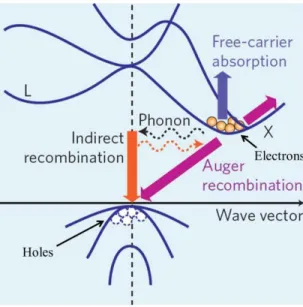
Light emission on silicon remains one of the biggest challenges. Indeed, Si being an indirect bandgap material, free electrons tend to relax in the X valleys of the conduction band whereas the free holes are located in the Γ valence band (see Fig. 1-1).
Thus, a radiative recombination between an electron and a hole can only occur if a third particule (a phonon) is involved in the mechanism to satisfy the momentum conservation. The poor light emission efficiency of Si is directly related to the low probability of such a three-particle event. At the same time, non-radiative processes are more likely to occur. Free-carrier absorption, wherein free electrons are promoted to higher conduction band levels by absorbing
photons, is the main mechanism preventing lasing from bulk Si12. Another common non-radiative
7 with a hole is gained by another electron (or a hole) which is promoted to a higher energy level. The internal quantum efficiency, which is defined by the ratio between the probability of a radiative recombination and the probability of any recombination, is thus very weak in bulk
silicon (10-6). We will now describe various approaches studied by many research teams in the
world to achieve lasing on silicon.
Fig. 1-1: Energy band structure of bulk Si and main carrier transition processes. From Ref. 11.
1.2 Laser emitters on silicon
1.2.1 Silicon-based sources
Using ultra-purity and optimized light extraction, Green et al. have demonstrated a light
emitting diode based on bulk Si13, but lasing in bulk Si has not been shown yet. To enhance the
radiative recombination, many research teams have been studying Si nanostructures14,15. Indeed,
if carriers are localized in a small region of real space, their wave functions are delocalized in the reciprocal space. Thus, the k-space selection rule responsible for the low efficiency in bulk Si, is
partially broken. Optical gain in Si nanocrystals embedded in a SiO2 matrix has been proved16,17.
The emitted light is red but the 1.55 µm telecommunications window can be reached by the
incorporation of Er ions15,18. The main issue of this approach is the electrical injection through
the SiO2 insulator. Although the electrical injection can be enhanced by tailoring the energy band
8
Another approach to achieve lasing emission in silicon aims at exploiting the stimulating
Raman scattering effect20. Room temperature continuous-wave pumping has even been achieved
by combining a ring cavity and a p-i-n structure to limit losses due to free carrier and two-photon
absorption21. Unfortunately, this technique needs a pumping laser which prevents any industrial
application.
1.2.2 Hybrid III-V/silicon lasers
If Si has been the material of microelectronics for sixty years, III-V compounds have undoubtedly been the materials of photonics. Indeed, since the first demonstrations of
semiconductor laser diode in 1962 (by Hall et al. for infrared wavelength22 and Holonyak et al.
for the visible range23), III-V direct band gap GaAs, InP, GaSb or GaN related compounds are
used in most of semiconductor laser diodes.
The heterogeneous integration of III‐V materials on a silicon wafer is one of the most advanced approaches to provide an efficient laser for integrated silicon photonics. III‐V heterostructures are first grown on their native substrates before being processed into individual dies which are afterwards individually bonded onto the Si platform (see Fig. 1-2).
Fig. 1-2: III-V dies bonded on a Si wafer. (CEA)
Bonding a complete III-V laser structure on Si substrate was first demonstrated by Wada
et al.24. Nevertheless, a special coupling scheme involving submicron precision alignment would
be required to integrate it with a PIC imbedded in a layer of Si. To deal with this issue, the group of J. Bowers in Santa Barbara has developed a technique which combines the bonding of thin
9
been working on this approach to improve bonding techniques26, to adjust the coupled optical
mode between the III-V active zone and the Si waveguide27 and to increase the compacity28.
Fig. 1-3: Evanescent coupling between a III-V active zone and a SOI waveguide. From Ref. 11.
This approach is considered by Intel as a very potent short-term solution to address the
medium volume applications of high-bandwidth data transmissions in servers and data centers29.
However, the reliability, the performance, the uniformity and the costs of this approach,
especially for high volume VLSI on-chip interconnects applications, are still unknown11,30.
1.2.3 Monolithic epitaxial lasers
On a longer term, monolithic integration of laser sources on silicon is expected to match more surely with the very large scale integration requirements. The monolithic approach consists in growing a light-emissive crystalline semiconductor structure onto the Si substrate. The main challenge of this approach is to reach a high quality crystalline structure, compatible with reliable laser devices (with a very low dislocation density). This is mainly prevented by the lattice constant mismatch between the semiconductors of the grown layers and the Si substrate. Indeed, the epitaxial growth of a semiconductor onto another, with different lattice constants, results in strain/stress energy accumulation in the layer. In this situation, if the lattice mismatch or the
thickness is too large, misfit dislocations appear during the growth to minimize the energy31,32.
These defects act as non-radiative recombination centers in the device. They actually add electrical resistance during the current flow through it, or limit the quantum efficiency of optical devices by decreasing the number of electron-hole pairs recombined in photons. Fig. 1-4 represents the energy of the band gap as a function of the lattice constant for the usual group IV and group III-V semiconductor compounds. It shows that most of the semiconductors classically
10
used for the photonics applications (GaAs, InP and their related compounds) cannot be lattice matched to Si. For a monolithic laser on Si, the main challenge is thus the improvement of the crystalline quality through the limitation of threading misfit dislocations in the grown structure (based on group IV or group III-V semiconductors) on Si.
Fig. 1-4: Bandgap energy of semiconductors as a function of their lattice constant. 1.2.3.1 Monolithic integration of group IV semiconductors
Using group IV semiconductors for integrated photonics on silicon is expected to have several technological advantages as compared with the monolithic integration of group III-V semiconductors. Indeed, growths of III-V and group IV semiconductors require two distinct chambers because of the cross-contamination and face the difficulty to deal with the intrinsic difference between crystallographic structures. Moreover, the monolithic integration of
modulators and photodetectors on Si has already been demonstrated using Ge based structures7-10.
For laser sources, the use of Ge is more difficult because of its indirect band gap. Nevertheless, as shown in Fig. 1-5, the difference between the L and the Γ conduction bands can be reduced by engineering the strain in Ge. A very high-doping level is then used to provide a significant
concentration of free electrons in the Γ conduction band33. Recently, the group of L. Kimerling in
MIT has demonstrated a room temperature, pulsed electrically pumped laser based on bulk Ge on
Si34. The 0.2% tensile strain has been achieved thanks to the difference in thermal expansion
coefficients between Ge and Si. Nevertheless, the threshold current density remains extremely
11
Fig. 1-5: Engineering of the band structure of Ge. From Ref. 33.
Another solution to engineer the band structure and get a direct band gap is the
incorporation of Sn to SiGe alloys35. But the issue of the lattice mismatching with Si still
remains. To try to limit the effects of the crystalline defects on the electrical and optical properties, the lattice constant can be progressively changed by growing composition graded
SiGe(Sn) buffer layer36. But this generally requires very thick layers (which are incompatible
with an evanescent coupling with a waveguide embedded in the silicon chip) and dislocations are not completely removed (which is incompatible with an electrical injection through the buffer layer).
1.2.3.2 Monolithic integration of III-V semiconductors on Si: the metamorphic approach
The idea of monolithically integrating III‐V materials on silicon is of course not new and first investigations already started in the 80’s with attempts in growing well-known GaAs or InP based structures. However, the direct growth of these materials is very difficult due to the polar/non-polar character of the III–V/Si interface, the mismatch of their respective lattice
constants (4 % for GaAs/Si and 8 % for InP/Si) and thermal expansion coefficients (2.6.10-6 K-1
for Si, 5.7.10-6 K-1 for GaAs, 4.6.10-6 K-1 for InP). Fig. 1-6 shows typical resulting dislocations in
a GaAs layer grown on Si. Although laser structures based on GaAs/AlGaAs QW or InGaAsP/InP QW have already been grown on Si, the very high density of dislocations
12
Fig. 1-6: Cross-sectional transmission electron microscope (TEM) image highlighting the dislocations in a GaAs layer grown on a Si substrate. From Ref. 42.
If crystalline defects cannot be totally prevented when growing lattice-mismatched layers, many research teams have developed strategies to try to confine the dislocations far away from the active zone. The use of strained short-period superlattices has been demonstrated to act
as a filter for dislocations42,43 (see Fig. 1-7(a)). On the same idea, the group of P. Bhattacharya
has developed a dislocations filter buffer layer based on InAs/GaAs QD (see Fig. 1-7(b)). Using this technique, encouraging results have been demonstrated with lasing structures exhibiting a
threshold current of 900 A.cm-2 under pulsed electrical pumping at room temperature44.
(a) (b)
Fig. 1-7: Cross-sectional TEM image of: (a) a threading dislocations filter based on strained-layer superlattices (SLS) and short-period superlattices (From Ref. 42) and (b) a blocked dislocation by a QD buffer
layer (From Ref. 44).
Another way to deal with the lattice-mismatch issue is the growth of the III-V structure on an oxide/Si layer such as SrTiO3/Si template. In principle, this technique should enable the III-V layer to immediately adopt its bulk lattice constant and thus prevent any threading
13 Another interesting approach to confine dislocations is the use of antimonide-based materials. As shown in Fig. 1-4, the lattice-mismatch between Si and III-Sb compounds is very large (12 % for GaSb/Si). But contrary to most of other III-V material systems, this very large lattice-mismatch is an advantage in the case of III-Sb material, since it is believed to be the main driving force for the formation of two-dimensional arrays of efficient strain-relieving misfit dislocations. Fig. 1-8 shows the relaxation of an AlSb layer by the formation of dislocations
confined at the AlSb/Si hetero-interface46. Using this AlSb nucleation layer and a GaSb fully
relaxed buffer layer, a laser diode operating at room temperature and under continuous-wave
electrical pumping has been demonstrated47. The wavelength is 2 µm and the threshold current
density is high (1.4 kA.cm-2). A structure emitting at 1.55 µm has also been achieved, but the
threshold current density is higher (5 kA.cm-2) and only pulsed regime has been demonstrated48.
Fig. 1-8: Cross-sectional TEM image of a two-dimensional dislocation network confined at the AlSb/Si interface. From Ref. 46.
The lowest room-temperature threshold current density for a metamorphic laser on Si has been achieved by the group of A. Seeds and H. Liu in the University College of London. Their idea is to benefit from both low threshold InAs/GaAs QD laser structure and significant improvements in crystalline quality of Ge on Si. Indeed, as shown in Fig. 1-4, the lattice-mismatch between GaAs and Ge is small (0.08 %). Moreover, their thermal expansion
coefficients are also very close (5.7.10-6 K-1 for GaAs and 5.9.10-6 K-1 for Ge). They have first
demonstrated an InAs/GaAs QD laser on Ge substrate operating at room temperature with a low
14
by a similar structure on Ge-on-Si substrate with threshold current densities of 163 A.cm-2
(continuous-wave operation) and 64.3 A.cm-2 (pulsed operation)50.
Nevertheless, the issue of all these approaches is that they resort to complex procedures and/or thick buffer layers which strongly limit the design flexibility for further device integration. A thick buffer layer prevents a simple coupling scheme with a photonic circuit embedded in the bottom Si chip. Moreover, driving the current through the dislocation layer is known to
dramatically deteriorate the electrical performances47.
Another solution to manage the strain relaxation without using buffer layers is to decrease the interaction between the grown layer and the substrate. This can be done by using
patterned substrates51 or by growing self-assembled one-dimensional nanostructures such as
nanowires, nanoneedles or nanopillars52–54. This approach enables the growth of lattice
mismatched materials without the formation of dislocations because of the large surface-to-volume ratio in the one-dimensional nanostructure, where the strain can be efficiently and
elastically relaxed55. Interesting results have been recently achieved by the group of C.
Chang-Hasnain in Berkeley56. They have demonstrated room temperature lasing of an InGaAs/GaAs
core-shell nanopillar with helically propagating cavity modes (see Fig. 1-9).
Fig. 1-9: III-V nanopillar grown on Si with an helically optical mode. From Ref. 58.
Due to the very small laser volume (6.10-13 cm-3), this approach is exciting for ultimate
integration of light source. Nevertheless, it faces various challenges. Electrically pumped lasers are missing even if light-emitting diodes with complex metallic contacts technology have been
15
shown57. Moreover, (111) oriented Si substrate are often used to favor the vertical growth of the
III-V structure. The control of the growth direction on more conventional (001) Si substrate is still challenging.
1.3 The pseudomorphic approach
The issue of the lattice-mismatch between III-V semiconductors and Si is often given as the main reason which has prevented the development of III-V laser on Si. To avoid the plastic relaxation which is the cause of device performances degradation, the layers can be grown coherently (pseudomorphically). This means that the in-plane lattice constant of the layers have to remain equal to the substrate lattice constant.
Fig. 1-10 is a zoom picture of Fig. 1-4 showing that GaP and AlP are the binary III-V semiconductors that have the smallest lattice-mismatch to Si (only 0.37 % for GaP/Si and 0.69 % for AlP/Si). Nevertheless, with a non-zero lattice-mismatch, a layer starts to relax plastically above the so-called critical thickness. Obviously, the smaller is the lattice-mismatch, the larger is the critical thickness. For GaP/Si, this value has been estimated to be in the range between 40 nm
and 100 nm59–61.A laser structure (including active zone and cladding layers) usually requires a
larger thickness (between 2 and 3 µm). Thus, compounds with even smaller lattice-mismatch to Si are needed.
Fig. 1-10: Bandgap energy of semiconductors as a function of their lattice constant. The blue (red) dotted line represents the dilute nitride (boron) GaPN (BGaP) alloy and highligths the perfect lattice-matching of
16
A perfect lattice-matching can be achieved with the incorporation of a small amount of nitrogen (2.2 % in GaP and 3.8 % in AlP at room temperature). Note that the lattice parameters of GaP, AlP and Si don’t have the same variation with temperature. This difference in thermal expansion coefficient should be compensated during the growth. Another solution is the use of boron. This second route is not studied in this thesis. Few reasons will be given in the following. The pseudomorphic approach which is studied in this thesis thus consists in developing laser structures with lattice-matched layers based on GaP(N) and AlP(N) related compounds. We will now briefly detail the various challenges of this approach.
1.3.1 Growth challenges
Even if the pseudomorphic approach is theoretically expected to result in a “defect free” structure, it still faces two main challenges: the III-V/Si interface and the growth of dilute nitride based laser device. These points are considered in the thesis work of Tra Nguyen Thanh, which has been jointly performed with the present work. Now we just briefly mention a few points related to this approach.
1.3.1.1 III-V/Si interface
Due to the amorphous character of SiN, a perfectly lattice-matched GaPN0.02 crystal
cannot be directly grown on Si substrate. The commonly widespread strategy is thus to grow a thin (below the critical thickness) GaP buffer layer on Si followed by a lattice-matched laser
structure based on dilute nitride alloys62,63.
Worldwide intense researches have been devoted to improve the crystalline quality of the GaP/Si interface and several research groups are on the verge to obtain defect-free GaP-on-Si
pseudo-substrate64–70. This is actually not straightforward because a defect-free growth means the
control and reduction of classical defects such as 3D growth, stacking faults or microtwins, but also of heterogeneous growth specific defects such as anti-phase boundaries (APB) and interfacial charge effects. The suppression (or at least annihilation) of these defects can be
achieved by an advanced optimization of the growth conditions64,66,67. The preparation of the Si
surface, in order to have a clean, flat and bi-atomic height stepped surface instead of mono-atomic steps, is one of the critical points, because it can totally prevent the APB formation. The use of Si(100) substrates which are slightly misoriented by a few degrees toward the [110]
17 direction is a route that has been followed by many research groups to favor Si bi-atomic height steps, even if this goal can be reached using conventional Si (001) substrates and carefully
selecting the substrate residual misorientation66,67,70,71.
The Foton laboratory strategy is to independently deal with the issues of GaP/Si interface and development of the III-V laser structure on GaP. This thesis is exclusively devoted to the development of the III-V laser structure, and that is the reason why many results are presented on GaP substrates in order to avoid the defects inherent to the GaP/Si interface.
1.3.1.2 Dilute nitride growth
The growth of dilute nitride alloys is very different from the growth of other III-V alloys. Two main reasons can be highlighted:
The crystal structure for the endpoints binary semiconductors (zinc-blende for phosphides
and arsenides and wurzite for nitrides) is different. This results in a very large miscibility gap, which means that the alloys are difficult to obtain without phase separation.
The equilibrium solid solubility of nitrogen is extremely low in phosphides as well as
arsenides ([N] < 1016 cm-3 in bulk GaP and [N] < 1014 cm-3 in bulk GaAs at T = 900 K)72.
In this context, efficient incorporation of nitrogen requires far from equilibrium growth conditions which are the case when using molecular beam epitaxy (MBE) or metal-organic chemical vapor deposition (MOCVD). From the sixties to the nineties, the incorporation of
nitrogen in GaP or GaAs was limited to doping regimes ([N] < 1019 cm-3). The incorporation of a
few percents of nitrogen in GaAs by MOCVD was achieved by the NTT labs in Japan in 199273.
In the same time, the incorporation of a few percents of nitrogen in GaP by MBE was
demonstrated by Baillargeon et al.74. Since, the N incorporation techniques have been improved,
especially with the use of novel N precursors for MOCVD (Dimethylhydrazine)75 or specially
designed plasma N2 source for MBE76,77.
Although many research groups have studied the growth of many dilute nitride alloys (GaAsN, GaPN, GaInAsN, GaAsPN, GaInAsSbN …) for the past fifteen years, achieving homogeneous and defect-free crystalline layers is still challenging. In dilute nitride alloys, the role of defects on the electronic and optical properties is enhanced, as compared to other semiconductors, due to the intrinsically large difference in size and chemical mismatch between
18
the N atom and the other V elements such as P or As. These defects give rise to deep levels in the band gap of alloys, which can act as limiting factor of optical properties. This issue has been
intensively studied both from the theoretical78,79 and experimental80–82 points of view. Among the
various N induced defects, N interstitials, Ga vacancies, Ga interstitials, As antisites have been experimentally identified in Ga(In)AsN, GaPN or GaAsPN alloys. The defects density can be
reduced by optimizing the growth conditions or performing post-growth annealing81,83,84. But a
general feature remains: the defects density tends to increase with the increasing of the N content. This is a result of both higher probability of generating such point defects and higher tendency in generating dislocations due to strain. Although N incorporation as high as 16 % has been reported
in GaPN85, reasonable concentrations for the optical devices we are developing in this thesis are
limited to a few percents (< 6 %)86,87.
1.3.2 Electronic structure challenges
We have seen at the beginning of this chapter that Si is not suitable for efficient laser emission because of its indirect band gap. Unfortunately, GaP and AlP also exhibit indirect band gaps. One of the main challenges of this thesis is thus to propose an efficient active zone.
The nitrogen incorporation, in dilute regimes, is known to strongly modify the electronic band structure and consequently the optical properties of arsenide, phosphide or antimonide alloys. A general feature that has been demonstrated in all dilute nitride alloys is the strong
reduction of the band gap with increasing N content, the so-called giant band gap bowing88–93.
The use of a dilute nitride alloy (GaInAsN) as a gain medium was first proposed by
Kondow et al.94. Indeed, this alloy can be lattice-matched to GaAs substrate and has enabled to
reach lasing emission at the wavelength of 1.3 µm on GaAs. For the pseudomorphic integration on Si, an alloy with a smaller lattice constant is required. We have seen that GaPN can adress the issue of lattice-mismatch. It has also been claimed that the incorporation of nitrogen in the
GaP1-xNx alloy would allow to reach a direct band gap for x > 0.5 %95. Unfortunately, the nature
of the band gap of GaPN is more complicated than a simple indirect-direct crossover and has been the subject of many controversies in the past decade. The issue is even more crucial for the GaAsPN alloy, for which much less studies exist. Yet, the only pseudomorphic laser structures
19 theoretical and experimental understandings of this alloy in order to give some routes for the improvements of laser characteristics.
Another challenge is to investigate other nanostructures for the active zone, which may be an alternative to poorly efficient GaAsPN QW existing laser structures. Moreover, the maximum of the emission wavelength reported for such structures with reasonable N content is
equal to 980 nm97, which is not yet in the transparency window of Si (above 1.1 µm). The use of
quantum dots is proposed because it allows the coherent growth of smaller band gaps materials nanostructures with larger lattice mismatch. Furthermore, due to their 0D confinement properties,
lower threshold currents have been demonstrated, in comparison to their QW counterparts98. The
InGaAsN/GaP QD system has been proposed by Fukami et al. as a good candidate99.
Nevertheless, very few studies have been performed on both InGaAsN/GaP QD and nitrogen-free InGaAs/GaP QD system.
Finally, another critical point for laser devices is the choice of cladding layers, whose role is to increase the overlap between the electromagnetic field and the gain region. In laser devices on GaAs substrate, AlGaAs cladding layers have been extensively used, because the incorporation of Al is known to strongly reduce the refractive index and AlAs and GaAs are quasi lattice-matched. By analogy, AlGaP based alloys are considered in this work. But the
striking difference with the AlAs/GaAs system is the type-II band alignment for AlP/GaP100. This
feature has to be carefully considered because it can reduce the confinement of carriers in the active zone.
1.3.3 Context of the pseudomorphic approach and positioning of Foton laboratory
Even if several research teams are working on the pseudomorphic approach, two of them can be highlighted, as they have succeeded in demonstrating operating devices on silicon.
The first one is installed in Philipps University Marburg, Germany, with a commercial showcase through the NAsP III/V GmbH Company. The first breakthrough demonstrated by this team was the achievement of room temperature lasing under electrical injection of GaAsPN
quantum wells on GaP substrate in 2006101. Although the laser characteristics which are shown
are limited (pulsed operation and a high threshold current density of 4 kA.cm-2)97; this is, to our
20
GaP/Si interface64, they recently gave a demonstration of GaAsPN QWs lasing on Si substrate up
to 150 K both optically and electrically96, and measured optical gain up to 300 K102. Nitrogen is
only incorporated in the quantum wells. The lattice-matching of barriers and cladding layers to Si, is ensured by the incorporation of boron in respectively BGaAsP and BGaP alloys. This growth strategy is conditioned by the use of MOCVD as the growth technique. Indeed, the compositional control and uniformity of dilute nitride layers is known to be harder to achieve with MOCVD as compared to MBE growth techniques; the most efficient dilute nitride based
devices (GaInNAs/GaAs lasers103 and tandem solar cells104) were presently demonstrated with
MBE. On the contrary, the incorporation of boron is more efficient with MOCVD thanks to the
use of triethyl boron precursor105. In the case of MBE, it is still challenging because of the very
low vapor pressure of solid B which requires very high cells temperature106.
The second team is based in Toyohashi University of Technology, Japan. They first demonstrated significant reduction of GaP-Si induced defects density in pseudomorphic layers in
1998107 by using an alternated growth procedure. This procedure is still being optimised66,108.
They achieved the MBE growth of GaPN lattice-matched to Si109. They demonstrated room
temperature LED devices on Si based on InGaPN/GaPN double heterostructure110 and
GaAsN/GaPN QW111, They finally demonstrated the ability to drive a GaPN LED by a p-type
metal oxide semiconductor field effect transistor (MOSFET) on Si112, which was the first
demonstration of real on-chip photonic integration, in the pseudomorphic integration.
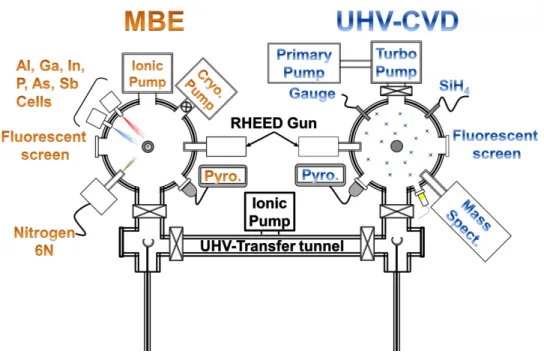
In this context, the FOTON laboratory started studying the growth of III-V heterostructures on GaP substrates by MBE in 2007. The incorporation of nitrogen has been enabled since 2009. Finally, a UHV-CVD (Ultra High Vacuum Chemical Vapor Deposition) chamber for the growth of group IV semiconductors has been installed during this thesis. The aim of this chamber is to grow a Si buffer layer with a surface as perfect as possible (with double atomic steps) prior to the growth of the III-V structure. A III-V solid source MBE chamber is connected through a ultra-high vacuum transfer tunnel. Group-III elements (Al, Ga and In) are generated from conventional effusion cells. Group-V elements (P, As, and Sb) are provided by
using valved cracker cells. Nitrogen is supplied using a valved RF plasma N2 source. Finally, Be
(p-type) and Si (n-type) are used as dopant sources. Fig. 1-11 shows a schematic of the UHVCVD-MBE growth cluster. The choice of the pseudomorphic approach was not conditioned
21 only by the need to integrate laser on Si. Indeed, since 2011, the FOTON laboratory has also been studying the development of multi-junction solar cells based on a Si bottom cell and a
lattice-matched GaAsPN top cell61,113. Finally, the growth of GaP on Si is expected to be interesting for
the integration of nonlinear optical functions. Indeed, GaP is an excellent candidate for second-order nonlinear processes because of its large indirect bandgap (2.35 eV), its large nonlinear
susceptibility (45 pm.V-1)114 and its large thermal conductivity (1.1 W.cm-1.K-1).
Fig. 1-11: UHVCVD-MBE growth cluster for III-V on Si integration. From Ref. 70.
1.4 Conclusion
In summary, we have seen that many approaches are worldwide proposed to demonstrate a laser on Si, each of them with its own benefits and drawbacks. None of them has clearly been standing out for now and complementary routes are most likely to emerge depending on the applications. The hybrid integration of III-V lasers on Si by bonding is probably going to address the medium volume applications of inter-chips optical communications. For VLSI applications, a monolithic laser is more desirable. The pseudomorphic approach may be one of the solutions as it prevents the high defect densities encountered in the growth of lattice-mismatched layers on Si. Nevertheless, it needs to deal with both growth challenges and efficient laser design. This latter point is developed in the following chapters.
22
References of Chapter 1
1 J. Bardeen and W.H. Brattain, Phys. Rev. 74, 230 (1948).
2 Int. Technol. Roadmap Semicond. Itrs (2012).
3 T. Tsuchizawa, K. Yamada, H. Fukuda, T. Watanabe, J. Takahashi, M. Takahashi, T. Shoji, E.
Tamechika, S. Itabashi, and H. Morita, Ieee J. Sel. Top. Quantum Electron. 11, 232 (2005).
4 N. Daldosso, M. Melchiorri, F. Riboli, M. Girardini, G. Pucker, M. Crivellari, P. Bellutti, A.
Lui, and L. Pavesi, J. Light. Technol. 22, 1734 (2004).
5 M. Ziebell, D. Marris-Morini, G. Rasigade, J.-M. Fédéli, P. Crozat, E. Cassan, D. Bouville, and
L. Vivien, Opt. Express 20, 10591 (2012).
6 G.T. Reed, G. Mashanovich, F.Y. Gardes, and D.J. Thomson, Nat Photon 4, 518 (2010).
7 P. Chaisakul, D. Marris-Morini, M.-S. Rouifed, G. Isella, D. Chrastina, J. Frigerio, X. Le Roux,
S. Edmond, J.-R. Coudevylle, and L. Vivien, Opt. Express 20, 3219 (2012).
8 Y.-H. Kuo, Y.K. Lee, Y. Ge, S. Ren, J.E. Roth, T.I. Kamins, D.A.B. Miller, and J.S. Harris,
Nature 437, 1334 (2005).
9 L. Vivien, J. Osmond, J.-M. Fédéli, D. Marris-Morini, P. Crozat, J.-F. Damlencourt, E. Cassan,
Y. Lecunff, and S. Laval, Opt. Express 17, 6252 (2009).
10 O. Fidaner, A.K. Okyay, J.E. Roth, R.K. Schaevitz, Y.-H. Kuo, K.C. Saraswat, J.S. Harris, and
D.A.B. Miller, Ieee Photonics Technol. Lett. 19, 1631 (2007).
11 D. Liang and J.E. Bowers, Nat. Photon. 4, 511 (2010).
12 W.P. Dumke, Phys. Rev. 127, 1559 (1962).
13 M.A. Green, J. Zhao, A. Wang, P.J. Reece, and M. Gal, Nature 412, 805 (2001).
14 M.J. Chen, J.L. Yen, J.Y. Li, J.F. Chang, S.C. Tsai, and C.S. Tsai, Appl. Phys. Lett. 84, 2163
(2004).
15 N. Daldosso and L. Pavesi, Laser Photonics Rev. 3, 508 (2009).
16 L. Dal Negro, M. Cazzanelli, B. Danese, L. Pavesi, F. Iacona, G. Franzò, and F. Priolo, J.
Appl. Phys. 96, 5747 (2004).
17 L. Pavesi, L.D. Negro, C. Mazzoleni, G. Franzò, and F. Priolo, Nature 408, 440 (2000).
18 S. Yerci, R. Li, and L. Dal Negro, Appl. Phys. Lett. 97, 081109 (2010).
19 A. Anopchenko, A. Marconi, M. Wang, G. Pucker, P. Bellutti, and L. Pavesi, Appl. Phys. Lett.
99, 181108 (2011).
20 H. Rong, A. Liu, R. Jones, O. Cohen, D. Hak, R. Nicolaescu, A. Fang, and M. Paniccia, Nature
433, 292 (2005).
21 H. Rong, Y.-H. Kuo, S. Xu, A. Liu, R. Jones, M. Paniccia, O. Cohen, and O. Raday, Opt.
Express 14, 6705 (2006).
22 R.N. Hall, G.E. Fenner, J.D. Kingsley, T.J. Soltys, and R.O. Carlson, Phys. Rev. Lett. 9, 366
(1962).
23 N. Holonyak and S.F. Bevacqua, Appl. Phys. Lett. 1, 82 (1962).
24 H. Wada and T. Kamijoh, Ieee Photonics Technol. Lett. 8, 173 (1996).
25 A.W. Fang, H. Park, O. Cohen, R. Jones, M.J. Paniccia, and J.E. Bowers, Opt. Express 14,
9203 (2006).
26 G. Roelkens, D. Van Thourhout, R. Baets, R. Nötzel, and M. Smit, Opt. Express 14, 8154
(2006).
27 M. Lamponi, S. Keyvaninia, C. Jany, F. Poingt, F. Lelarge, G. de Valicourt, G. Roelkens, D.
Van Thourhout, S. Messaoudene, J.-M. Fedeli, and G.H. Duan, Ieee Photonics Technol. Lett. 24, 76 (2012).
23
28 D. Liang, M. Fiorentino, T. Okumura, H.-H. Chang, D.T. Spencer, Y.-H. Kuo, A.W. Fang, D.
Dai, R.G. Beausoleil, and J.E. Bowers, Opt. Express 17, 20355 (2009).
29 M. Paniccia, Nat. Photonics 4, 498 (2010).
30 P. Cheben, R. Soref, D. Lockwood, and G. Reed, Adv. Opt. Technol. 2008, 1 (2008).
31 J. Weertman and J.R. Weertman, Elementary Dislocation Theory (Macmillan, 1964).
32 J.W. Matthews and A.E. Blakeslee, J. Cryst. Growth 27, 118 (1974).
33 J. Liu, L.C. Kimerling, and J. Michel, Semicond. Sci. Technol. 27, 094006 (2012).
34 R.E. Camacho-Aguilera, Y. Cai, N. Patel, J.T. Bessette, M. Romagnoli, L.C. Kimerling, and J.
Michel, Opt. Express 20, 11316 (2012).
35 P. Moontragoon, R.A. Soref, and Z. Ikonic, J. Appl. Phys. 112, 073106 (2012).
36 M.T. Currie, S.B. Samavedam, T.A. Langdo, C.W. Leitz, and E.A. Fitzgerald, Appl. Phys.
Lett. 72, 1718 (1998).
37 J.P. van der Ziel, R.D. Dupuis, R.A. Logan, and C.J. Pinzone, Appl. Phys. Lett. 51, 89 (1987).
38 M. Razeghi, M. Defour, R. Blondeau, F. Omnes, P. Maurel, O. Acher, F. Brillouet, J.C. C‐Fan,
and J. Salerno, Appl. Phys. Lett. 53, 2389 (1988).
39 M. Sugo, H. Mori, Y. Sakai, and Y. Itoh, Appl. Phys. Lett. 60, 472 (1992).
40 T. Egawa, Y. Murata, T. Jimbo, and M. Umeno, Photonics Technol. Lett. Ieee 9, 872 (1997).
41 T. Yamada, M. Tachikawa, T. Sasaki, H. Mori, and Y. Kadota, Appl. Phys. Lett. 70, 1614
(1997).
42 I.J. Luxmoore, R. Toro, O.D. Pozo-Zamudio, N.A. Wasley, E.A. Chekhovich, A.M. Sanchez,
R. Beanland, A.M. Fox, M.S. Skolnick, H.Y. Liu, and A.I. Tartakovskii, Sci. Reports 3, (2013).
43 K. Samonji, H. Yonezu, Y. Takagi, K. Iwaki, N. Ohshima, J.K. Shin, and K. Pak, Appl. Phys.
Lett. 69, 100 (1996).
44 Z. Mi, J. Yang, P. Bhattacharya, G. Qin, and Z. Ma, Proc. Ieee 97, 1239 (2009).
45 B. Gobaut, J. Penuelas, J. Cheng, A. Chettaoui, L. Largeau, G. Hollinger, and G. Saint-Girons,
Appl. Phys. Lett. 97, 201908 (2010).
46 S.H. Huang, G. Balakrishnan, A. Khoshakhlagh, L.R. Dawson, and D.L. Huffaker, Appl. Phys.
Lett. 93, 071102 (2008).
47 J.R. Reboul, L. Cerutti, J.B. Rodriguez, P. Grech, and E. Tournié, Appl. Phys. Lett. 99, 121113
(2011).
48 L. Cerutti, J.B. Rodriguez, and E. Tournie, Ieee Photonics Technol. Lett. 22, 553 (2010).
49 H. Liu, T. Wang, Q. Jiang, R. Hogg, F. Tutu, F. Pozzi, and A. Seeds, Nat. Photonics 5, 416
(2011).
50 A. Lee, Q. Jiang, M. Tang, A. Seeds, and H. Liu, Opt. Express 20, 22181 (2012).
51 C.V. Falub, H. von Känel, F. Isa, R. Bergamaschini, A. Marzegalli, D. Chrastina, G. Isella, E.
Müller, P. Niedermann, and L. Miglio, Science 335, 1330 (2012).
52 T. Mårtensson, C.P.T. Svensson, B.A. Wacaser, M.W. Larsson, W. Seifert, K. Deppert, A.
Gustafsson, L.R. Wallenberg, and L. Samuelson, Nano Lett. 4, 1987 (2004).
53 J. Tatebayashi, A. Lin, P.S. Wong, R.F. Hick, and D.L. Huffaker, J. Appl. Phys. 108, 034315
(2010).
54 M.H.H. Alouane, N. Chauvin, H. Khmissi, K. Naji, B. Ilahi, H. Maaref, G. Patriarche, M.
Gendry, and C. Bru-Chevallier, Nanotechnology 24, 035704 (2013).
55 M. Montazeri, M. Fickenscher, L.M. Smith, H.E. Jackson, J. Yarrison-Rice, J.H. Kang, Q.
Gao, H.H. Tan, C. Jagadish, Y. Guo, J. Zou, M.-E. Pistol, and C.E. Pryor, Nano Lett. 10, 880 (2010).
56 R. Chen, T.-T.D. Tran, K.W. Ng, W.S. Ko, L.C. Chuang, F.G. Sedgwick, and C.