HAL Id: hal-00473023
https://hal.archives-ouvertes.fr/hal-00473023
Submitted on 13 Apr 2010HAL is a multi-disciplinary open access
archive for the deposit and dissemination of sci-entific research documents, whether they are pub-lished or not. The documents may come from teaching and research institutions in France or
L’archive ouverte pluridisciplinaire HAL, est destinée au dépôt et à la diffusion de documents scientifiques de niveau recherche, publiés ou non, émanant des établissements d’enseignement et de recherche français ou étrangers, des laboratoires
Local detection of the optical magnetic field in the near
zone of dielectric samples
E. Devaux, Alain Dereux, E. Bourillot, J. C. Weeber, Y. Lacroute, J. P.
Goudonnet, Christian Girard
To cite this version:
E. Devaux, Alain Dereux, E. Bourillot, J. C. Weeber, Y. Lacroute, et al.. Local detection of the optical magnetic field in the near zone of dielectric samples. Physical Review B: Condensed Matter and Materials Physics (1998-2015), American Physical Society, 2000, 62 (15), pp.10504–10514. �hal-00473023�
To be published in Phys. Rev. B
Local detection of the optical magnetic field in the near zone of
dielectric samples
Elo¨ıse Devaux, Alain Dereux, Eric Bourillot, Jean-Claude Weeber, Yvon Lacroute, Jean-Pierre Goudonnet
Laboratoire de Physique, Optique Submicronique, Universit´e de Bourgogne, BP 47870, F-21078 Dijon, France
Christian Girard
Centre d’Elaboration des Mat´eriaux et d’Etudes Structurales, 29 rue J. Marvig, BP 4347, F-31055 Toulouse, France
(May 18, 2000)
Abstract
We present a study of the influence of the probe composition on the formation of constant height Photon Scanning Tunneling Microscope (PSTM) images when observing a dielectric sample. Dramatic effects due to the metallization of the tip are presented and discussed in details. We show how the recorded images can look quite different when the probe is dielectric or coated with gold. Comparison with numerical calculations indicate that the experimental signals are of electric or magnetic nature depending on the composition of the tip. For well-defined conditions, gold coated tips provide images of the distribution of the magnetic field intensity associated with the optical near-field. To get more insight into the origin of this intriguing effect, we have performed a careful analysis of the plasmon modes associated with a gold coated dielectric
cylinder. We conclude that the detection of the optical magnetic field is related to the conditions of excitation of circular symmetry plasmon, or ring plasmon, in the gold coated tip.
07.79.Fc,73.20.Mf,78.66-w
I. INTRODUCTION
In optical near–field devices1
, the local detection of the optical signal relies on the use of nanometer–sized probes. These probes are generally sharpened optical fibers which are em-ployed in two basic configurations. In the generic Scanning Near-Field Optical Microscope (SNOM) configuration, the probe acts as a local source of evanescent optical fields, while in the generic Photon Scanning Tunneling Microscope (PSTM) setup2
, the probe behaves as a local detector of light. In order to achieve a narrower localization of the incident light on the sample surface, SNOM tips are usually coated with a thin metal layer. For this purpose, Al is the most widely used metal, although very few works have been devoted to the influence of various tip compositions when observing a given reference sample using a SNOM setup3
. By analogy, it was believed that a proper metal coating of the tips would also improve the resolution of the PSTM configuration. However, the first PSTM attempts using Al coated tips have shown a limited improvement due to the concommitent degradation of the signal to noise ratio related to the very low transmission through such a coating. In order to re-duce this noise, fully gold coated tips (with no resulting apertures at the apex) were recently experimented4
. Surprisingly, it turned then out that these probes recorded isointensity im-ages with an inverted contrast relatively to the contrast obtained with (uncoated) dielectric tips. These results have clearly indicated that the detected signal may reveal different phys-ical phenomena according to the probes composition. Calculations of magnetic or electric field maps, at constant height above a well-defined sample4–6
have allowed to interpret these different kinds of contrasts. While the dielectric tip always collects a signal proportional to the square modulus of the electric near-field, the images recorded at the incident wavelength λ = 633 nm, for a well–defined gold thickness on the probe, display the same patterns than the theoretical maps of the square modulus of the magnetic field associated with the optical near–field. However, the first experiments suggesting a possible detection of the magnetic field4,5
raised several important questions to which we intend to answer in the present work. In this paper, we precise the conditions for the occurence of this phenomenon by
pro-ceeding to a systematic study of a well–defined dielectric sample in various experimental configurations. In sections IV and V, we discuss a series of PSTM images we have obtained with different probe tips (uncoated or fully coated), at two different incident wavelengths and for both transverse magnetic and transverse electric incident polarizations. Our analysis confirms the possibility to detect, in well–defined conditions, the optical magnetic near-field with gold coated tips. Moreover, the results also provide new indications about the effective height of detection in PSTM experiments.
A licit hypothesis, already mentionned in reference 4, suggests that the magnetic field detection could be justified by the existence of plasmon eigenmodes in the fully coated tip, at the red laser frequency (λ = 633 nm) used in the first experiments. More precisely, it was assumed that these plasmons could be able to radiate a net optical energy proportionally to the optical magnetic field scattered or confined by the sample structures. Since the excitation of a plasmon depends strongly on geometrical features, we have examined two geometries which could possibly account for this particular detection process. First, we may assume that the red laser frequency excites a small gold particle at the apex of the tip. Alternatively, the gold coating around the dielectric core has a circular symmetry, which may sustain a particular collective motion of the electron gas of the metal. It would then give rise to a circular symmetry plasmon, an expression that we shorten by “ring plasmon”. We have discarded the first hypothesis because the red laser frequency is not a surface plasmon eigenfrequency of a spherical gold particle having the dimensions of the apex of the tip7,8
. To check the second geometry, we have modeled this apex by a thin dielectric cylinder coated with gold and calculated the dispersion relation of plasmons associated to such a geometry. Section VI demonstrates that the red laser frequency is indeed a plasmon eigen-frequency of this tip model for radii and optical properties corresponding to those of the tips used in the experiments. A first experimental test of this hypothesis appears in Sec. VII A where we present images recorded with “semi-coated” probes which are obtained by depositing an assymetric metallic layer around the dielectric core. Indeed, if the detection of the magnetic field is related to the circular symmetry of the collective excitation around
the core, it should not occur if the symmetry conditions are broken. We effectively observed that semi-coated probes behave like (uncoated) dielectric ones.
As a second experimental check to support the model of coated cylinder, we have repeated the detection of the optical magnetic field at another wavelength (λ = 543 nm) on the basis of the ring plasmon resonance conditions in the probe coating. From the dispersion relation of the coated cylinder model, we have adjusted the gold coating thickness in order to excite a ring plasmon at λ = 543 nm. At this wavelength and with the preset value of the gold coating on the tip, we obtained the same contrast than a calculated map of the square modulus of the magnetic field again (section VII B). For very precise experimental parameters, we thus succeeded in reproducing the phenomenon of magnetic field detection from the hypothesis of the existence of a ring plasmon sustained by the gold coating. Moreover, the detection of the optical magnetic field with gold coated tips was surprisingly found to be equally efficient as the detection of the optical electric field with bare dielectric tips provided that the conditions of plasmon excitation are satisfied.
II. EXPERIMENTAL SETUP
We use a D3000 scanning force microscope (Digital Instruments) in which the AFM cantilever is replaced by a sharpened optical fiber when it is used in the PSTM configuration. This fiber tip is brought piezoelectrically close to the sample surface and behaves like a local probe. The sample is illuminated in total internal reflection and most of the intensity collected by the fiber corresponds to the evanescent part of the light scattered by its surface. Different lasers have been used to observe the influence of the wavelength of the incident light on the recorded images : a red laser (wavelength λ = 633 nm) and a green laser (λ = 543 nm). A polarizer is placed between the laser and the prism on which the sample lies.
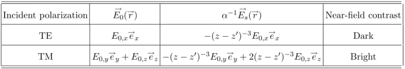
An AFM image of a typical dielectric sample we have studied appears on fig. 1. Seven glass pads deposited on a glass substrate are the result of a microfabrication process based on electron beam lithography. Their lateral size is about 130 nm and their height is about
100 nm. The closest distance between two pads is 900 nm. This pattern is reproduced every 20 µm along horizontal lines on the sample surface. This has allowed us to scan on different patterns and explains the differences (defects, incomplete patterns,...) which can be observed on the various experimental images reported in this paper. Indeed, in the case of a tip-crash, we had to change the zone scanned by the probe. The glass substrate has the same index of refraction as the prism on which it lies.
The images have been recorded in constant height mode (512 x 512 pixels), which is possible by tuning the gain of the electronic feedback. The gray scale of the experimental images presented in this paper thus corresponds to the variations of the detected intensity in a plane parallel to the sample surface (no auxiliary force feedback). The amplification of the signal upon using the green laser had to be increased because it was less powerful than the red one. Therefore, the images recorded at λ = 543 nm were somewhat noisy. We have filtered this noise by the Savitzky-Golay algorithm which allows to smooth the data with a minimal broadening9
. For each series of images, the tip is approached as close as possible to the sample, until the contact occurs. By “series”, we mean that we have used the same tip, the same incident wavelength and the same polarization of the laser. A series is thus the sequence of images recorded at different setpoints of the near-field microscope, where each successive setpoint brings the tip apex at a smaller constant height above the sample surface.
Since, as shown in previous works4,11
, the optical response is not necessarily bright above a pad, we need to know the localization of the pads relatively to the observed optical response. In order to avoid artefacts related to any kind of auxiliary force feedback10
, the only reliable way to localize a pad is to note where the tip touches first the surface in the near-field image. Indeed, the tip will fatally crash into one of the pads as one reduces the constant height of scan above the surface. Most of the images we present here have been recorded presumably a few nanometers above the pads, at the last setpoint which allowed scanning without crashing into one pad. Any arrow reported in the image of this paper indicates where the tip crashed when scanning at the next smaller height. This procedure
relies on a tip production facility delivering at high rate well reproducible tip designs. The probes we used for this work are multimodes fibers which are sharpened by pulling. Such probes are not so sharp as those used in references 4 and 11 which were obtained by chemical etching, but they are more reproducible. After the pulling, the fiber can be placed in a calibrated evaporator where it is fully coated (no resulting aperture at the apex) with gold while turning around its axis. The deposition process has a 1 nm accuracy determined by a device relying on the use of a quartz weighing apparatus.
III. THE GREEN’S DYADIC METHOD AS AN INTERPRETATION TOOL
The contrast observed in the images can be interpreted thanks to numerical simulations. Indeed, previous PSTM works11,12
have established that dielectric tips detect the electric field associated with the optical wave close to the sample surface because the observed contrasts correspond to the square modulus of the electric field distribution, as given by the solution of Maxwell equations which does not include the tip. In order to understand the contrasts of the experimental constant-height images, we keep following the principle of finding the relation between the experimental images and the solution of Maxwell equations, as computed in the absence of the tip. For the sake of our demonstration, we just need reliable theoretical constant height maps of the electric and magnetic near-fields distributions which can be considered like the images due to a point-like detector. For this purpose, we used a numerical solver which computes the electromagnetic near-field distribution in a plane parallel to the sample surface, when it is illuminated in total internal reflection by polarized light. It is based on the Green’s dyadic method13–15
, which is proven to be an efficient computation technique for the typical parameters of near-field optics. The input geometry of the computations was given by an AFM data file recorded previously on the sample (fig. 1). These data are discretized by cubic cells of 30 nm ×30 nm ×30 nm . The illumination conditions are chosen as follows : θ = 60o
(angle of incidence in the prism) and ψ = 90o
not so well controlled since it depends on the initial orientation of the sample on the prism. It may also be modified by a misalignement of the patterns on the substrate. In all the calculations, the detected intensity is calculated in a plane which is located at a constant height zref above the sample surface, without accounting for the tip. It is then normalized
to the calculated intensity at the same height when there is no pad on the surface of the glass substrate.
According to the state of polarization of the incident light and to the composition of the tip, the contrasts of the images change dramatically. Following a procedure detailed recently in reference 12, we have searched the value zref resulting in the best agreement with the
experimental images. In order to reproduce their contrasts when they are recorded with dielectric tips, a different value of zref is required according to the state of polarization: we
found zref = 150 nm for the TM incident polarization and zref around 200 nm for the TE
incident polarization. Some of the images recorded with gold coated tips have been compared to magnetic field intensity maps. For both incident polarizations, the best agreement was found near the observation plane located at zref = 130 nm.
The short-range parts of the propagators of the electric22,14
and magnetic6
fields can be used to understand the origin of the PSTM contrast at the immediate proximity of the dielectric pads. Let us assume that a given pad is discretized by a single cell located at r
→′ = (0, 0, z′). Within the first Born approximation and with the harmonic time dependence,
the total field E(r→ →) at a point r→= (0, 0, z) is given by13
: → E(r→) = →E 0(r→) + → Es(r→) ≈ → E0(r→) + S ↔0 (r→− r→′)V (r→′)→E 0(r→′) (1)
whereE→0(r→) is the electric field incident under the condition of total internal reflection and
V (r→′) is the perturbation expressing the fact that the pad on the surface creates a dielectric
function contrast. The constant α having the dimension of a volume, one can approximate the short-range propagator14
of the electric field S↔0
↔ S′0(0, 0, z − z′)V (r→′) ≈ α −(z − z′)−3 0 0 0 −(z − z′)−3 0 0 0 (z − z′)−3 (2)
Therefore, the scattered field E→s(r→) represents the modification of →
E0(r→) due to the
perturbation V (r→′). Table I gives the components of E→
s(r→) and the contrasts which are
expected to be observed on an experimental PSTM image. For example, when the incident field is TE polarized, the scattered electric field has a negative sign. In the near-field zone, a dark contrast is then associated to the total electric field which is less intense than the incident field. For a TM polarized field, the magnitude of E→0,y is smaller than
→
E0,z. The
resulting bright near-field contrast is mainly due to the z component of the scattered electric field which turns out to be positive and is enhanced by a factor two.
A similar approach may be followed when reasoning on the basis of the magnetic part of the incident optical waveH→0(r→). In this case, we use once again the first Born approximation.
The total magnetic field H(r→ →) is then given by:
→ H(r→) =H→ 0(r→) + → Hs(r→) ≈ → H0(r→) + ↔ Q0 (r→− r→′)V (r→′)H→ 0(r→′) (3) whereQ↔0
(r→− r→′) is the short-range propagator of the magnetic field6
. The constant β having the dimension of an area, the short-range approximation leads to:
↔ Q0 (0, 0, z − z′)V (r→′) ≈ β 0 −(z − z′)−2 0 (z − z′)−2 0 0 0 0 0 (4)
The components of the scattered magnetic field H→s(r→) are given in table II, together with
the near-field contrasts they produce. For a fixed state of polarization (TE or TM) of the incident field, one notices that an inversion of the contrast right above the pads is expected between an electric and a magnetic field map. Furthermore, the propagator of the electric field S↔0
decreases as (z − z′)−3 whereas the propagator of the magnetic field Q↔0
decreases as (z − z′)−2. Thus, at a short distance (z − z′) from the surface, the magnetic intensity
decay is smoother than the electric intensity. These results, provided by the examination of the short-range parts of the propagators S↔0
andQ↔0
, are useful to interpret the experimental images. However, we stress the fact that all short and long range terms of the propagators are fully taken into account in all numerical calculations given in the following sections.
IV. DIELECTRIC TIPS
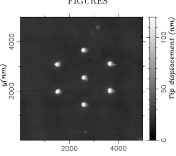
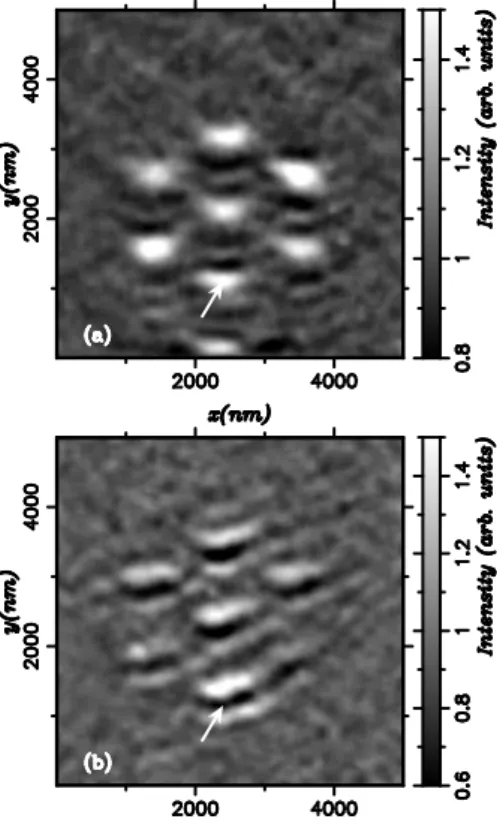
To obtain reference images for later comparisons, we have first experimented uncoated dielectric tips. For TE incident polarization, the Green’s dyadic method predicts a negative (dark) optical response above nanoscopic objects (section III, table I). During an exper-iment, when the tip was approached a few nanometers closer to the sample to perform a scan at the next lower constant height, the tip crash into one of the pads occured in the dark parts of the optical response, as indicated by the arrows on fig. 3a (λ = 543 nm) and fig. 3c (λ = 633 nm). This tip crash feature was checked to be reproducible with several tips imaging different seven-pads patterns reproduced on the sample surface. At this stage, two important points must be underlined. First, these dark contrasts are similar to those already observed by using chemically etched tips scanning the surface in the isointensity mode11
. Second, in this work, using pulled tips and working in the constant height mode leads to a significant broadening of the near–field patterns. In particular, the confined peaks close to the pads, reported in reference 11, can not be observed anymore.
In order to interpret the experimental images of figs. 3a and 3c, two electric field maps computed in an observation plane zref = 200 nm are given in fig. 4. A narrower dark signal
and the confined peaks, similar to the isointensity measurements of reference 11, come out of the calculations if the map is computed at a height closer to the sample, i.e., with zref ≤ 150
nm. Since the etched tips used in11
are sharper than the pulled ones, it thus seems that the mean detection plane is lower for etched tips than for pulled tips. The absence of confined peaks when using pulled tips may be understood by the fact that, not only the short-range part, but also the other terms of the electric field propagator start to be significant in the
calculations when the height of detection zref increases to over 150 nm above the sample,
involving this slight modification of the near-field contrast14,16
.
For the TM incident polarization, the differences with the images presented in11
are limited to a more important broadening when using pulled tips. In this polarization, the tip has touched the bright lobes when it was scanning very close to the surface. It means that the optical responses right over the pads are positive for both wavelengths (fig. 3b, 3d), as expected from table I, and as confirmed by the calculated electric field map (fig. 4b).
Computed field maps for both incident polarizations present different aspects compared to the experimental images: sharper interferences patterns and better localization of the optical responses. They are explained by the simplifications that have been done in the calculations. In particular, not including the tip is equivalent to a pointlike detector. In the experiment, the electric intensity is integrated by the finite size of the tip. It results in smoother interferences patterns and broader signals above the pads. Moreover, in the calculations, the surface around the pads (inside but also outside the computation window) is assumed to be perfectly flat. In a realistic experiment, there may be many others small structures on the sample surface (protrusions, dusts, ...). The multiple scattering of the incident surface wave by these structures can also attenuate the interferences of surface waves. We can thus conclude that the near–field feature which can be reliably compared to theoretical maps is the intensity contrast right above the pads.
V. GOLD COATED TIPS
Using tips coated with 20 nm of gold provides PSTM images which are sensitive to the incident wavelength. To analyze this singular behavior, two different wavelengths have been considered:
(i) As shown in fig. 5a and 5b, when working with a green incident light (λ = 543 nm) we have not observed significant changes relatively to the electric field pattern |E|→2
which is detected with a pure dielectric tip. The dependence of the contrast right above the pads
on the incident polarization confirms that the detected signal is of electric nature.
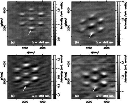
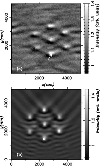
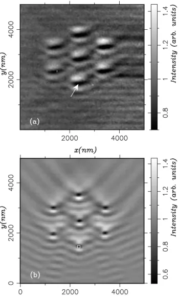
(ii) When illuminating the sample with the second wavelength λ = 633 nm, we observed a dramatic evolution of the images for both incident polarizations (fig. 6a and fig. 7a). For example, in the TE mode, the pads appears now with a bright contrast and the TM images reveal them with a very neat and dark contrast. In this last case, the dark signal right above the pads are surrounded by two bright lobes located perpendicularly to the direction of propagation of the incident surface wave. The localization of the pads was checked with the tip crash test explained above. Specifically, for TM incident polarization, the tip touched the sample between the two lobes. Thus, for this wavelength λ = 633 nm, the images do not fit in with the optical electric intensity anymore. Indeed, these images do not agree with the simulations presented on fig. 4, where the detected intensity was supposed to be proportional to |E|→ 2
.
In order to explain this constrast reversal phenomena, we can make use of the data gathered in the table II which indicate similar contrast changes when passing from |E|→ 2
to |H|→ 2
intensities. To check this hypothesis, we have therefore calculated the magnetic field maps above the sample, for both polarizations. These maps (fig. 6b and 7b) look quite similar to the images recorded at λ = 633 nm with a tip coated with 20 nm of gold (fig. 6a and 7a). We have checked that a linear superposition of both electric and magnetic fields, with equal weights, can not give such strongly varying contrast. The squares showing the underlying position of the lower pad on the theoretical maps confirm the inversion of the contrasts. It means that the signal detected in this case is proportional to |H|→ 2
. The magnetic field maps have been calculated at the same height above the sample, i.e. zref = 130 nm
for both states of polarization. Moreover, the width of the optical responses is as good as on the images presented in reference 4 which had been recorded with etched fibers. Here again, we can interpret this thanks to the considerations given in section III, where we have seen that the short-range decay of the magnetic near-field intensity follows a z−2 law while
the short-range decay of the electric near-field intensity follows a z−3 law. The short-range
the short-range behaviour of the intensity of the electric field. Therefore, even if the tips have not the same mean plane of detection according to their different fabrication process (etched in reference 4 or pulled in the present work), they provide the same kind of results when detecting the magnetic field because the values of zref are not at the validity edge of
the short-range approximation of the magnetic field propagator Q↔0.
VI. MODELLING GOLD COATED TIPS
A. Mixed susceptibility
As already mentionned in the introduction, the most probable hypothesis able to account for the detection of optical magnetic field intensity relies on the excitation of plasmons resonances in the tip at the wavelength operated in the experiment. Indeed, these plasmons could lead to the excitation of a magnetic moment entering the mixed susceptibility tensor
↔
Υtip of the tip. In fact, this mixed susceptibility is a dyadic function which describes how
the tip responds linearly to the magnetic near–field according to:
µ
→(r→) = ↔Υ tip·
→
H(r→) (5)
where µ→(r→) is the fluctuating electric moment of the plasmon. Moreover, Υ↔
tip displays
resonances for eigenfrequencies of the system, as well-known in the context of molecular physics17
. In the present situation, such resonant mixed susceptibility inside the detector could explain our results. To get more insight into this complex phenomenon, we will schematize the detector with two different model geometries.
B. Small gold sphere
In this case, it is well–know from standard textbooks (see for example reference 8) that the magnetic moment of a small spherical particle is proportional to the factor
∆(ω) = ( ǫ(ω) − 1 2ǫ(ω) + 3 ) , (6)
where ǫ(ω) is the dielectric function of gold, and ω = 2πc/λ is the angular frequency of light in vacuum. The factor ∆(ω) displays a resonance when ǫ(ω) = −1.5. In the case of gold spheres in vacuum, this resonance occurs around the wavelength λ = 465 nm (8). The proximity of the glass substrate is well–known to induce a red–shift of this resonance wavelength. In order to provide an excess value of this effect, we suppose that the gold sphere is fully embedded in glass in which case it is easy to find that the resonance is red– shifted towards the wavelength λ = 502 nm. We may thus conclude, that in spite of this overestimated red–shift, the shifted resonance wavelength of a spherical particle remains very far from the incident wavelength λ = 633 nm for which the magnetic field detection effect has been observed. Consequently, the model of a resonating particle at the apex of the fully coated tip must be discarded.
C. Gold coated glass cylinder
We then assumed a second model based on the approximation of the tip by a gold coated glass cylinder (fig. 9). In order to know if the gold coated tip may sustain a plasmon resonance, we have calculated the dispersion relation of the surface plasmon modes18
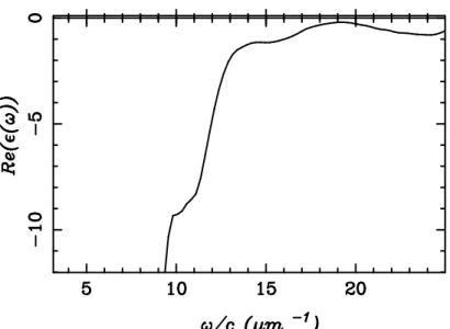
of such a geometry. The gold coating thickness may be defined by the difference d between the outside a and inside b radii (fig. 9). The wavelength dependent values of the gold dielectric response ǫ(ω) were found in reference21
. The validity of this set of data was assessed in reference12
to predict the occurence of plasmon resonances of nanoscopic structures (gold nanowires and nanodots deposited on glass) which were then observed experimentally at the right wavelength and at the right location with a PSTM. The dielectric functions are ǫC = 2.25 in the glass core and ǫA = 1 in the external medium. The time-dependence
of fields were chosen harmonic. The small dimensions of the tips allow to neglect the retardation effects. According to a standard procedure19,20
, we solved the Laplace equation for the electric potential in cylindrical coordinates (ρ, φ, z) and searched the surface modes, decaying for growing radial distance ρ and oscillatory as a function of z and φ. We found
the dispersion relation of the surface eigenmodes of a gold coated dielectric cylinder to be: ǫA K′ m(akz) Km(akz) − ǫ(ω)I ′ m(akz) Im(akz) ! ǫC I′ m(bkz) Im(bkz) − ǫ(ω)K ′ m(bkz) Km(bkz) ! = I ′ m(bkz)Km′ (akz) Im(akz)Km(bkz) (ǫ(ω) − ǫA)(ǫ(ω) − ǫC) (7)
In this expression, Im, Km are the modified Bessel functions of the first and second kinds
respectively while I′
m, Km′ are their first derivatives. kz is the projection of the wave vector
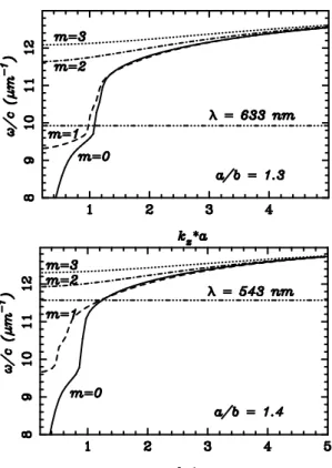
along the longitudinal (z) axis of the cylinder. The angular dependence of the solutions is exp imφ. Since dispersion relations describe ideal, undamped, normal modes, the roots of the above equation are computed, as usual, by zeroing the imaginary part of the dielectric function of the metal (ǫ(ω)), i.e. by taking only the real part of ǫ(ω) into account. The results of such computation are zero-width dispersion curves for each value of m (fig. 10). Finite lifetime effects related to the imaginary part of ǫ(ω) broaden these dispersion curves. Therefore, when two curves related to different values of m are sufficiently close to each other, the said broadening related to the imaginary part of ǫ(ω) allows to consider both curves as overlapping.
In the above dispersion relation, the argument of the Bessel functions depends implicitly on the ratio a/b. Dispersion curves have been computed systematically for a/b ratios covering ranges of values which are relevant in the context of this paper. For values of kza smaller than
1 or close to 1 (which correspond to the range of validity of the non-retarded approximation), this systematic study brings to the fore a main difference between gold cylinders (b = 0) and glass cylinders coated with gold (b 6= 0). In the dispersion relation of gold cylinders (not shown), the m = 0 curve enters alone the range of red frequencies and that an important frequency gap separates this m = 0 curve from the m ≥ 1 curves which arise at higher frequencies. For glass cylinders coated with gold, it turns out that, according to the value of the ratio a/b, the m = 0 and m = 1 curves may both enter the range of red frequencies (fig. 10). Since the abcissae of the dispersion curves is the product of kz multiplied by
the outside radius a, such dispersion curves actually describe a discrete spectrum for each specific gold coated glass cylinder defined by the radii a and b. Due to this discrete nature
of the plasmon spectrum and since the photons are well-known to carry unit spins which are exchanged in interactions of light with matter, the elastic coupling of red light to the plasmon field requires that both m = 0 and m = 1 curves do virtually overlap each other.
We therefore searched which ratio a/b results in m = 0 and m = 1 curves sufficiently close to each other at the angular frequency of the red He-Ne laser (wavelength in vacuum λ = 633 nm) so that they are practically overlapping by virtue of the above mentionned broadening effect. This does occur for a/b = 1.3 which sets a = 100 nm and d = 23 nm (fig. 10). These values are in good agreement with the dimensions of the real tips: indeed, according to the fabrication parameters, the gold coating thickness was about 20 nm in the experiment while the mean radius at the tip apex was around 100 nm. But for the green laser (λ = 543 nm in vacuum), the dispersion curve for the ratio a/b = 1.3 implies that a = 146 nm and d = 33 nm. According to this model, the tips coated with d = 20 nm, leading to the same contrast on the images than the purely dielectric tips, do not sustain any plasmon resonance at λ = 543 nm.
For the actual dimensions of the tips (a ≈ 100 nm and d ≈ 20 nm), we can conclude from the dispersion curves that, at λ = 633 nm, a plasmon excitation associated to the ring geometry can be sustained by the gold coating. We postulate that the mixed polarizability
↔
Υtip of this nanoscopic ring could be resonant in our experiment. The plasmon could then
radiate proportionally to the optical magnetic field, thereby leading to an image pattern which is proportional to |H|→ 2
. At λ = 543 nm, the conditions of plasmon resonance are not fulfilled and the optical magnetic field detection should not occur if d = 20 nm. However, the cylinder shaped tip being a rough model, we decided to check experimentally the dependence of the optical magnetic field detection on the circular symmetry plasmons associated with the cylinder geometry.
VII. EXPERIMENTAL CONFIRMATION OF CIRCULAR SYMMETRY PLASMONS
A. Semi-coated tips
For each ratio a/b, a family of ring plasmons can be excited and these particular modes depend basically on the circular symmetry of the metallic coating. Now, a “semi-coated” tip, obtained by the evaporation of a dissymetric gold layer on the dielectric core, not only downgrades the effective ratio a/b but additionnaly breaks the circular symmetry. If a ring plasmon is involved in the detection of the optical magnetic field, breaking this fundamental symmetry should not lead to detect |H|→ 2
. On the contrary, if a semi-coated tip still detects the same signal, we should conclude that this particular detection is related to another process. The semi-coated tips are fabricated in the same manner as described in Sec. II, but they are not rotated in the evaporator, while the deposition time is reduced in order to coat only one side of the tip with 20 nm of gold. With this procedure, in spite of some gold atoms diffusion effects on the other side of the tip, the resulting metal layer is always highly dissymmetric. To ensure that no particular effect due to this dissymetry could happen, we recorded the images with two orientations of the gold coated side with respect to k→//(see fig.
11). At λ = 633 nm, for the TM incident polarization, the contrast is the same with both orientations (fig. 12). Moreover, the images look like if they were recorded with a purely dielectric tip. They reveal the same contrast than the figure 3b with a signal proportional to |E|→2
. These results support our hypothesis: the circular symmetry of the gold coating being broken, the semi-coated probes do not collect a magnetic signal anymore. This definitely discards the excitation of a single gold particle as the possible cause of the detection of the optical magnetic field. Incidentally, we can notice that the broadening of the bright spots is reduced with these tips (fig. 12), relatively to the use of dielectric tips (fig. 3b): the resolution, defined relatively to the distribution of |E|→2
, is thus improved by semi-coated tips.
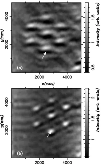
B. Optical magnetic field detection at λ = 543 nm
The next attempt we made to confirm the role of ring plasmons in detecting a magnetic signal with a PSTM was to reproduce the phenomenon at another incident wavelength. We chose to determine the conditions leading to a plasmon excitation at λ = 543 nm for another value of the ratio a/b. For a/b = 1.4, we notice (fig. 10) that the m = 0 and m = 1 curves are well separated in the range of red frequencies but start to overlap each other for a value of the frequency corresponding to the wavelength in vacuum λ = 543 nm. The intersection of both m = 0 and m = 1 curves with the straight line λ = 543 nm defines the values a = 96 nm and d = 29 nm. This is not so far from the estimated value of the outside radius a = 100 nm which was the basis of our modelling in section VI. The fibers used in this section have then been placed a longer time in the evaporator, in order to obtain a layer of 30 nm of gold around the dielectric core. The images recorded with this kind of probes, while the sample was illuminated with the green laser, are presented in fig. 13. The contrasts right above the pads obtained with both incident polarizations are the same than those recorded recorded at λ = 633 nm using a probe coated with 20 nm of gold (fig. 6a and 7a), that is, the same than on the theoretical magnetic field mapspresented on fig. 6b and 7b. When the wavelength of the incident light is changed to be 633 nm, other experiments (not shown) have checked that such tips coated with 30 nm of gold do not detect a signal proportional to |H|→ 2
anymore but collect a signal proportional to |E|→2
.
The gold coated glass cylinder model of the tip turns out to be sufficient to define the conditions leading to the detection of the optical magnetic field with another design of the PSTM probe. The hypothesis of the excitation of a ring plasmon is thus relevant to account for the process of detecting optical magnetic fields. Furthermore, we can state that a magnetic signal is collected by the tip only for very accurate parameters. Indeed, we have finally fabricated a coated tip by evaporating 35 nm of gold. It means that the gold layer around the tip was 5 nm thicker than on the tip used to record fig. 13. For TM incident polarization and at λ = 543 nm again, the pads have appeared in bright contrast (fig. 14),
in the same way than with a dielectric tip (fig. 1a). The conditions of resonance have thus been broken by the addition of only a few nanometers of gold.
VIII. CONCLUSION
The experiments presented in this paper confirm that the composition of a PSTM probe may influence dramatically the nature of the detected signals. Specifically, for well-defined wavelengths and precise coating thicknesses, gold coated glass tips allow signals proportional to the optical magnetic field intensity to be detected in the near–field zone.
A theoretical analysis based on an elementary model of coated cylindrical glass tip indi-cates the possible excitation of ring plasmons in the metal layer surrounding the dielectric core. In each situation where the detection of the optical magnetic field occurs, these circular symmetry plasmon modes are active.
As proven by the utilization of “semi-coated” tips, the circular symmetry of the gold coating appears to be fundamental for observing the phenomenon. The experimental evi-dence thus suggests that plasmons associated to a ring geometry might set up significant dynamical magnetic field detection processes that can mask the more common electric field detection mechanisms. Through the above mentioned resonant phenomena, ring plasmons could radiate energy proportionally to the incident optical magnetic field intensity, thereby explaining the observations reported in this paper. This work thus calls for a deeper theo-retical analysis of the properties of plasmons in nanoscopic rings.
ACKNOWLEDGMENTS
We thank Y. Chen (CNRS, Bagneux) for providing the sample. Stimulating discussions with U. Ch. Fischer and T. L. Ferrell are gratefully acknowledged. This work was supported by the Regional Council of Burgundy, by the CNRS through the Ultimatech research pro-gram and by the specific research propro-gram about nanotechnologies initiated by the French Ministry for Education and Research.
REFERENCES
1
D. Courjon, C. Bainier, Rep. Prog. Phys. 57, 989 (1994).
2
R. C. Reddick, T. L. Ferrell, R. J. Warmack, Phys. Rev. B 39, 767 (1989).
3
Note added in proofs: After the submission of this paper, a quantitative study of the influence of the Al coating thickness of SNOM tips on illumination mode near-field optical microscopy images was published by L. J. Richter, C. E. Jordan, R. R. Cavanagh, G. W. Bryant, A. Liu, S. J. Stranick, C. D. Keating, M. J. Natan, J. Opt. Soc. Am. A 16, 1936 (1999).
4
J.C. Weeber, PhD Thesis, University of Burgundy (Dijon, 1996).
5
A. Dereux, E. Bourillot, J.C. Weeber, J.P. Goudonnet, Y. Chen, C. Girard, Ann. Phys. Fr. 23, 27 (1998).
6
C. Girard, J.C. Weeber, A. Dereux, Phys. Rev. B 55, 16487 (1997).
7
C. F. Bohren and D. R. Huffman, Absorption and scattering of light by small particles (Wiley, New-York, 1983).
8
J. A. Stratton, Electromagnetic theory (Mac Graw Hill, New-York, 1941).
9
W. H. Press, S. A. Teukolsky, W. T. Vetterling, B. P. Flannery, Numerical Recipes in Fortran (Cambridge, 1992).
10
B. Hecht et al., J. Appl. Phys. 81, 2492 (1997).
11
J.C. Weeber, E. Bourillot, A. Dereux, J.P. Goudonnet, Y. Chen, C. Girard, Phys. Rev. Lett. 77, 5332 (1996).
12
J.R. Krenn, A. Dereux, J.C. Weeber., E. Bourillot, Y. Lacroute, J. P. Goudonnet, G. Schider, W. Gotschy, A. Leitner, F. R. Aussenegg, C. Girard, Phys. Rev. Lett. 82, (1999).
13
14
O. J. F. Martin, C. Girard, A. Dereux, Phys. Rev. Lett. 74, 526 (1995).
15
C. Girard, A. Dereux, O. J. F. Martin, M. Devel, Phys. Rev. B 50, 14467 (1994).
16
C. Girard, D. Courjon, Phys. Rev. B 42, 9340 (1990).
17
A. D. Buckingham, Advan. Chem. Phys. 12, 107 (1967).
18
A.D. Boardman, Electromagnetic surface modes (Wiley, New-York, 1982).
19
K. L. Kliewer and R. Fuchs, Adv. in Chem. Phys. 27, 355 (1974).
20
C. A. Pfeiffer, E. N. Economou, K. L. Ngai, Phys. Rev. B 10, 3038 (1974).
21
E.D. Palik, Handbook of optical constants of solids (Academic, New-York, 1984).
22
TABLES
TABLE I. When modelling a nanoscopic dielectric pad by a single discretization cell and keep-ing only the (approximated) short-range part of the electric field propagator, components of the scattered electric field E→s( r→) as a function of the polarization of the incident field
→
E0( r→). e→ j, (j = x, y, z) are the unit vectors in Cartesian coordinates such that e→
z is perpendicular to the sample surface.
Incident polarization E0( r→ →) α−1E→
s( r→) Near-field contrast
TE E0,x→ex −(z − z′)−3E0,x→ex Dark
TM E0,y→ey + E0,z→ez −(z − z′)−3E0,y→ey+ 2(z − z′)−3E0,z→ez Bright
TABLE II. When modelling a nanoscopic dielectric pad by a single discretization cell and keeping only the (approximated) short-range part of the magnetic field propagator, components of the scattered magnetic field H→s( r→) as a function of the polarization of the incident field
→ H0( r→). e
→
j, (j = x, y, z) are the unit vectors in Cartesian coordinates such that e→z is perpendicular to the sample surface.
Incident polarization H0( r→ →) β−1H→
s( r→) Near-field contrast TE H0,y→ey+ H0,z→ez (z − z′)−2H0,y→ex Bright
FIGURES
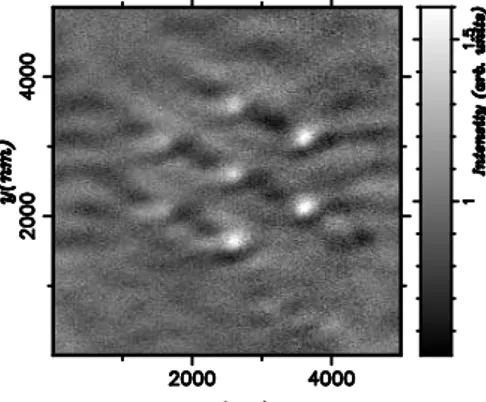
FIG. 1. AFM image of the sample. Tracks close to the pads, along the scanning direction are due to the presence of water on the sample.
k// y k θ ψ z x
FIG. 2. Definition of the angles θ (angle of incidence) and ψ (azimuthal angle). In the PSTM experiments presented in this paper, their values are θ = 60o
(total internal reflection) and ψ = 90o , i.e. k→// along y.
FIG. 3. Experimental constant height PSTM images recorded with dielectric tips at the last height which allowed scanning without crashing into the sample, for both wavelengths (λ = 543 nm and λ = 633 nm) and both incident polarizations TE ((a) and (c)) and TM ((b) and (d)). The arrows indicate where the tips crashed when scanning at the next smaller height.
FIG. 4. Theoretical distribution of |→E|2
at λ = 633 nm for (a) TE (zref = 200 nm) and (b) TM (zref = 150 nm) incident polarizations. The same contrasts are obtained with λ = 543 nm. On all the theoretical field maps, a little white square shows the position of the pad which is at the bottom of the pattern. Its coordinates were taken from the discretized AFM data file which have been used for the calculations.
FIG. 5. Experimental constant height PSTM images recorded with a gold coated tip (d = 20 nm) and λ = 543 nm: (a) TE incident polarization, (b) TM incident polarization.
FIG. 6. For λ = 633 nm and TE incident polarization: (a) constant height experimental PSTM image recorded with a gold coated tip (d = 20 nm); (b) theoretical distribution of |H|→2
(zref = 130 nm).
FIG. 7. For λ = 633 nm and TM incident polarization: (a) constant height experimental PSTM image recorded with a gold coated tip (d = 20 nm); (b) theoretical distribution of |H|→2
(zref = 130 nm).
FIG. 8. Real part Re(ǫ(ω)) of the dielectric function of gold as a function of ω as tabulated in reference21 eρ eφ a-b=d e 2b 2a ez e e y z x
FIG. 9. Model for the gold coated tip: a cylindrical dielectric core of radius b is uniformly coated by a thickness d = a − b of gold. e→
FIG. 10. For the geometry of a glass cylinder of radius b coated with a thickness d = b − a of gold, dispersion curves of the m = 0, 1, 2, 3 branches of plasmon modes for the ratios a/b = 1.3 and a/b = 1.4. As m increases, the branches converge to a horizontal line (not drawn) defined by ω/c = ωs/c, where ωs is such that ǫC = −ǫ(ωs), corresponding to the non-retarded dispersion relation of a flat glass-gold interface. The straight lines (− · · · −) are guides for the eyes in order to locate easily the two laser frequencies (here converted in units of wavelength in vacuum) operated in the experiments reported in this paper.
ey ez ex k // Core ey ez ex k // Core Coating (a) (b)
FIG. 11. Sketch of the two lightning conditions of the semi-coated tips used in this work. The e→i (i = x, y, z) are the units vectors in Cartesian coordinates, which are consistent with the coordinates system of the experimental images introduced in fig. 2. k→// is the component of the incident wavevector which is parallel to the sample surface.
FIG. 12. Experimental constant height PSTM image recorded with a semi-coated tip in the configuration (a) presented on fig. 11 (λ = 633 nm, TM incident polarization). The configuration (b) of fig. 11 leads to the same contrast.
FIG. 13. Experimental constant height PSTM image recorded with a gold coated tip (d = 30 nm) at λ = 543 nm: (a) TE incident polarization, (b) TM incident polarization.
FIG. 14. Experimental constant height PSTM image recorded with a gold coated tip (d = 35 nm) at λ = 543 nm for a TM incident polarization.