HAL Id: hal-02415466
https://hal.archives-ouvertes.fr/hal-02415466
Submitted on 9 Mar 2020
HAL is a multi-disciplinary open access
archive for the deposit and dissemination of
sci-entific research documents, whether they are
pub-lished or not. The documents may come from
teaching and research institutions in France or
abroad, or from public or private research centers.
L’archive ouverte pluridisciplinaire HAL, est
destinée au dépôt et à la diffusion de documents
scientifiques de niveau recherche, publiés ou non,
émanant des établissements d’enseignement et de
recherche français ou étrangers, des laboratoires
publics ou privés.
The light behavior from Shallow Trench Isolation
profiles at Chemical Mechanical Planarization step and
correlation with optical endpoint system by
interferometry
Sophia Bourzgui, Gaelle Georges, Agnès Roussy, Jakey Blue, Emilie Faivre,
Jacques Pinaton
To cite this version:
Sophia Bourzgui, Gaelle Georges, Agnès Roussy, Jakey Blue, Emilie Faivre, et al.. The light behavior
from Shallow Trench Isolation profiles at Chemical Mechanical Planarization step and correlation with
optical endpoint system by interferometry. Reflection, Scattering, and Diffraction from Surfaces VI,
Aug 2018, San Diego, United States. pp.11, �10.1117/12.2320966�. �hal-02415466�
The light behavior from Shallow Trench Isolation profiles at Chemical
Mechanical Planarization step and correlation with optical endpoint
system by interferometry
S. Bourzgui
a,b,c, G. Georges
a, A. Roussy
b, J. Blue
b, E. Faivre
c, J. Pinaton
c aAix Marseille Univ, CNRS, Centrale Marseille, Institut Fresnel, Marseille, France;
b
Mines Saint-Etienne and LIMOS, UMR CNRS 6158, CMP Georges Charpak, F-13541 Gardanne,
France;
c
STMicroelectronics, Rousset, France
ABSTRACT
In the semiconductor manufacturing, the control of Chemical-Mechanical Planarization (CMP) process time for Shallow Trench Isolation (STI) is important. A wafer under- or over-polishing causes leakage and short-circuits making the chips defective. The CMP process control by interferometry is one of the most used systems to monitor the polishing time. In some cases, the interferometry process control is not possible because the wafer patterns cause some unwanted effects such as scattering, diffraction, and absorption. Consequently the signal is affected. In this paper, we apply a theoretical and experimental approach on the light reflected from different STI stacks in order to interpret the observed optical phenomenon. The experimental study is done to get close to the light measurement conditions within the manufacturing environment. With this experiment, we evidence that the trench pattern inside memory zones is responsible for the diffraction effect on the signal. In a production environment, this pattern results in a lower measured intensity when the size of memory area increases. Besides, numerical calculations are performed based on differential method in order to predict the diffracted intensity, which depends on the chip design parameters and the incident wavelengths tuning. By using STI models, this method helps to determine the wavelengths with the highest reflected intensity.
Keywords: optical endpoint detection, interferometry, CMP, STI stack profile, wafer pattern, diffraction, scattering,
wavelength.
1.
INTRODUCTION
1.1 STI CMP process control
STI CMP process is essential to create the right Step Height (SH) of silicon dioxide (SiO2) to separate electrically the
transistors implemented later in the fabrication process (Fig.1). Thus in order to remove the right amount of SiO2
thickness, the process requires a reliable system to control the material removal at nanometer accuracy. One of the most relevant process control widely used for CMP is the optical endpoint detection, with a monochromatic laser source1-3 or,
for advanced nodes a white-light source4.
In this paper, the focus is made on the endpoint detection by interferometry for STI CMP process. Light interferences enable to correlate the SiO2 thickness with the intensity detected during polishing time. Thus the sinusoid signal obtained
is used to stop at the SiO2 thickness target wanted. To achieve it, a detection algorithm is created. It is composed of two
key elements: filters to smooth the raw signal and detection windows to detect sinusoid slopes. Nevertheless, the signal must be sufficiently intense and with a correct amplitude to achieve process control by the optical system. The interferometric signal ideally presents a perfect sinusoid. In a context of polishing, it is noisy by the wafer patterns and the movements of the polishing process, such as the platen rotation, the head rotation and head sweep. In some cases, this signal does not have the necessary conditions for the correct detection and this paper is aimed at this category of products.
Previous researches and experimental results5 illustrate that the interferometric signal shape strongly depends of the
noise ratio. Such of signals can prevent from creation of a robust detection algorithm and thus the use of the endpoint detection by interferometry.
The objective here is to study the light reflected upon STI profiles and to investigate the associated optical effects such as scattering and diffraction. With the understanding of these effects, it is possible to highlight the incident light behaviors according to the product parameters. Thus, the goal is to make some analogy between the results and the poor detection in production. In addition, in order to find a configuration for better signal detection, calculations are made on the visible band and near infrared. This part of the research allows us to see the evolution of light intensity as a function of product parameters and ranges of wavelength. So, the goal is to give a range of wavelengths which are better suited to a given SiO2 thickness and trench depth combination.
1.2 Context
The STI CMP is composed of three polishing steps, performed by three different platens, each of them having a specific objective: the platen 1 is responsible for polishing the most of the SiO2 layer and leaving 100nm of SiO2 thickness above
the Si3N4. The platen 2 removes the SiO2 remaining above the Si3N4. Finally the platen 3 slightly polishes the Si3N4 to
overcome any residual oxide problem on the active areas (Fig. 1.a). As part of this study, the process control by interferometry is used to polish SiO2 on the platen 1. The method is based on the optical interference of the laser beam
reflections from the interface of a semi-transparent material layer. The optical system is positioned under the polishing platen and the red laser beam crosses a transparent window (Fig. 2).
a) b)
1.3 Purpose
In this previous experimental research5, a Design Of Experiment (DOE) has studied the impact on signal shape of three
key product features at the STI manufacturing step: memory size, SiO2 thickness before STI CMP and trench depth (see
Fig. 3). It demonstrates two significant observations about the influence of product parameters on signal shape:
- At the scale of the chip, the bigger the memory zone is, the larger the noise and the smaller the amplitude are. The important feature of memory design is that a periodic grid of SiO2 trenches structures it.
- For a given memory size, the trench depth is the main influent parameter on amplitude of sinusoid signal. Fig. 1: Schematic representations of cross-sectional views of the materials stack at the CMP STI step for a) and the stack after the
Si3N4 removal and the SH between the Si and the SiO2 STI for b).
As it shows in the Fig. 4, the largest memory sizes have a signal with weak amplitude, and prevent from the creation of detection algorithm. Nonetheless, the previous study shows that the signal can be improved by varying two key parameters: deposited SiO2 thickness and the trench depth, in a hundred-nanometer scale. However, this result does not
give information about the optical phenomenon associated with the light reflected upon different STI stack profiles and, at which wavelength it could have higher signal intensity.
a) b) c)
Fig. 2: The graphs show filtered memory products’ signals. Each curve represents the signal intensity during the polishing process of platen 1. The a) has the smallest memory size, b) an intermediate size and c) the largest memory size. For a), the signal is correct for developing the detection algorithm in contrast to b) and c) which have poor endpoint detection.
So this paper presents theoretical and experimental approaches to respond to these interrogations. In a first part, the experimental study is presented, set up with the light measurement conditions close to the manufacturing environment. To complete, numerical calculations based on differential method are performed to predict the diffracted intensity as a function of the chip design parameters and of the incident wavelengths. Used on STI models, this method helps to determine the wavelengths with the highest reflected intensity. The conclusions to this research will give directions of future works, about the necessity of topology characterization and the possibility to adapt the STI topology.
2.
EXPERIMENTAL STUDY
2.1 Angular Resolved Scatterometer
To analyze the laser source behavior reflected at the wafer surface, the experimental study is carried out using an Angular Resolved Scatterometer developed at the Fresnel Institute6-10. The light source used for this experiment is a laser
He-Ne at 632.8 nm. The incidence angle is 45°. To have the same wafer illumination surface conditions, the beam shape is widened with the use of a beam expander, and then the source passes through the same window used for the polishing process. Figure 5 shows a scheme of the measurement device.
Fig. 1: The diagram shows that microchips are made up of several types of pattern like memory zones which have a periodic structure of trenches with high density, compared to logic zone.
2.2 Samples
Wafer samples measured are composed of three different memory sizes. Reflecting spectra is collected as a function of the angle, from (-10°) to 60°.
Table 1: Samples and characteristics associated
Sample n° 1 2 3
Optical process control YES NO NO
Memory size (kbits) 32 512 2048
% of memory coverage/chip 10 53 70
As said previously, the objective of this experiment is to determine the optical phenomena associated with mono-chromatic laser on the wafer surface. The method used to determine scattering or diffraction is based on the results obtained by the light intensity over the angle.
2.3 Results of light diffraction from a laser source (λ = 632.8nm)
The Fig. 6 a) highlights the intensity measurement in function of the scattering angle for three memory sizes, with an identical trench depth. Apart from the diffraction orders, the scattered light is close to zero. This result shows that the light scattering by the STI profiles is negligible. Thus the surface roughness should have a little impact on the reflected light loss in production.
a) b)
Fig. 4: Chart a) shows the normalized intensity detected as a function of scattering angle. The first order corresponds to the beam diffraction caused by the periodicity of the sample patterns. Graph b) shows the result of the laser intensity average per wafer during polishing process from the same three types of samples.
To add, the measured intensities of samples 2 and 3 present diffraction at the first order. Using the grating equation (1), the experimental result of the distance between successive grooves responsible of the first diffracted order is calculated11.
(1) - nair: air refractive index (1)
- m: diffraction order (-1) - λ: laser wavelength (632.8 nm) - i: incidence angle (-45°) - r: refractive angle (-3°)
The experimental result of the groove spacing is expressed as a value normalized by a reference surface S. The experimental result a/S = 33.32 nm-1 is closed to the theoretical size of a trench period in the memory area: a/S = 33.60
nm-1. The path period calculation highlights that the pattern responsible for the diffraction is the dimension of a trench
period in memory zone. This experiment shows that the light behavior is different according to the percentage of memory zone and logical zone in the chip. With a memory that covers 10% of the chip, it is the light and logic zone interaction that predominates. In contrast to memories covering a larger chip area, it is the interaction between light and memory zone that predominates. Moreover, the diffraction reduced the intensity of the signal reflection. Measures of average intensities in production shows that the interferometric signal decreases as the memory size increases (see Fig. 6 b).
To complete these experimental measures, the second part presents which conditions would be more favorable to increase the reflected intensity by numerical calculations and by making the focus on periodical structures in memory zone.
3.
THEORITICAL STUDY
3.1 Description
The simulation code, initially developed in the Fresnel Institute9, calculates the intensity diffracted by any
two-dimensional profile using the differential methods. This code makes it possible to simulate the interaction of an incident wave with periodic or random structures, and, therefore, in this case to take into account the variation of different parameters of the microstructures (the trench depth and the deposit SiO2 thickness). Thus, the calculations are made in
the range of visible and near-infrared range with a step of 10nm.
To perform the simulation, it is first necessary to create a model of the STI stack. In order to be the most precise in the shapes of material each layer, wafers cross sections before and after polishing were done. The Scanning Electron Microscopy (SEM) images made from its sections allowed reproducing a model that is as close as possible to reality in terms of thickness and shape of the different layers. On the other hand, the refractive indices n and k for each material must be defined to calculate the diffracted intensity. The n and k calculation is performed with the Cauchy-Urbach formula12-13:
(2)
- An, Bn and Cn: index parameters,
- Ak: extinction coefficient amplitude,
- b: the exponent factor, - Eg: the band edge
The coefficients are measured on a Semilab ellipsometer14, on a wafer with STI stacking before polishing with a fit
quality of R² = 0.99.
Table 2: Coefficient values for n and k calculation
n k Si3N4 An 2.00E+00 1.45E+00 Bn (μm²) 1.25E-02 4.20E-03 Cn (μm4) 7.00E-05 1.40E-07 SiO2 Ak 6.53E-02 4.47E-02
b(1/eV) 6.19E+00 1.12E+00 Eg(eV) 8.21E+00 6.43E+00
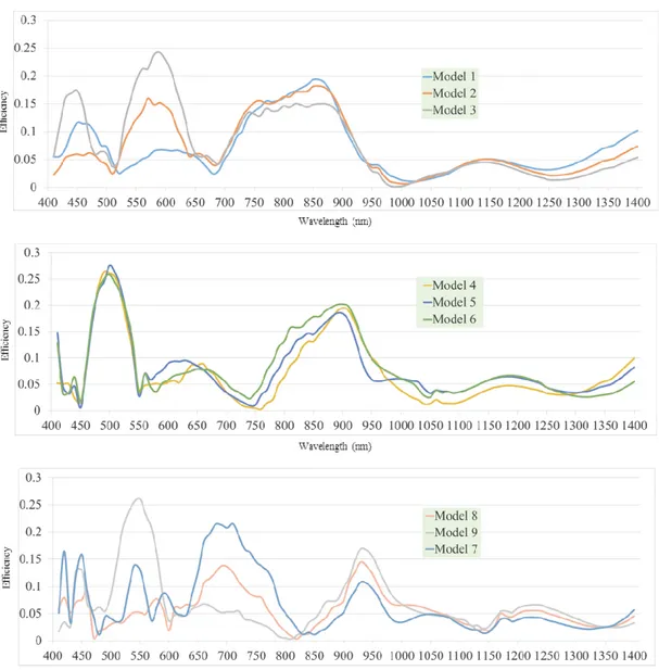
Besides, the substrate considered is a silicon substrate and the superstrate is air. The model size is ten micrometers and the calculation is done in two dimensions. Nine models are built, with different trench depths and SiO2 thicknesses:
Table 3: STI models
Model SiO2 thickness (nm) Trench depth (nm)
1 650 535 2 650 575 3 650 615 4 720 535 5 720 575 6 720 615 7 800 535 8 800 575 9 800 615
The purpose of these calculations is therefore to study the behavior of the reflected light in the periodic trench structures and to extract the wavelengths with the highest order 0 intensity.
3.2 Results from the calculations
Numerical calculations give the result of the efficiency as a function of the scattering angle. From these results, the light reflected at the order 0 is extracted. This light reflected at the order 0 is expressed as a function of the wavelength to thus study the wavelengths with the maximum reflected intensity. Each curve in Fig. 7 corresponds to a STI model and the nine models are divided into three graphs. In the same graph, the deposited SiO2 thickness is identical.
First, all models have a reflected intensity, for wavelengths above 990nm, lower compared to the rest of the light spectrum. This wavelength range is obviously not optimal for maximizing the intensity of the reflected signal. For endpoint detection, the wavelength used is in the range of red. The calculation results of the intensity as a function of the wavelength show that the red range is not the optimal zone in terms of intensity reflected at the order 0 with an efficiency around 0.05. This result is valid for all models except the 7 model, with an efficiency around 0.2 (four times greater). However, during polishing, the thickness of SiO2 decreases. It is therefore essential that the reflected intensity is also
optimized at the lower SiO2 deposits. Models 4 and 1 are models equivalent to Model 7 with the same trench depth and a
lower deposit, but a low efficiency value. We must therefore find a compromise between a high efficiency and a deposit thick enough to have a good planarization. Indeed, the trench period is a parameter that cannot be modified because it would change the properties of the device. However, the SiO2 deposit can be modified, while respecting a ratio of SiO2
thickness on trench depth acceptable for polishing. Models 7 to 9 with the thickest deposit (800nm) do not show peak efficiency at the same wavelengths as the other models with lower SiO2 deposition. Taking as SiO2 thickness before
CMP at 720nm, we are therefore looking for models 1 to 6 with efficiency peaks at the same wavelengths. For optimizing the intensity of the measured signal for models 1 to 6, the reflected intensity around the 870nm wavelength is about three times as much as in the red range. In conclusion, for product with large zones of periodic structures, to
maximize the signal intensity and improve the signal-to-noise ratio for endpoint detection, the recommended wavelength in these calculations is around 870nm, for a SiO2 thickness before CMP at 720nm.
4.
CONCLUSION
The purpose of this study is to complete the results of previous experiments, which shows that the size of the memories has an impact on the interferometric signal used as a process control for STI CMP. On one hand, the goal of this work is to analyze the origin of the light loss for the products with large memory. On the other hand, to propose an experimental set up that maximizes the signal, and improves the signal-to-noise ratio for endpoint detection. Thus, with the experiment, it has been possible to demonstrate that the periodicity of SiO2 trenches in memory zone diffracts the
incident light, when these areas reach a certain percentage of the entire chip. The diffraction might be the cause of the intensity loss of the reflected beam at order 0 and the deterioration of the signal-to-noise ratio. In addition, numerical calculation of the intensity reflected on STI profiles of a memory zone has shown that in other wavelength range, especially around 870nm, the reflected signal is 3 times more intense. However, calculations are limited to small structures and do not take into account logic zone inside the chip. Thus, it would be interesting to go further in this study by measuring the same type of products with the selected wavelengths.
REFERENCES
[1] Dale L. Hetherington, David J. Stein, "In-line monitoring of chemical-mechanical polishing processes", Proc. SPIE 3884, In-Line Methods and Monitors for Process and Yield Improvement, (27 August 1999)
[2] S. J. Fang et al., "Control of dielectric chemical mechanical polishing (CMP) using an interferometry based endpoint sensor," Proceedings of the IEEE 1998 International Interconnect Technology Conference (Cat. No.98EX102), San Francisco, CA, 1998, pp. 76-78.
[3] D. A. Chan, B. Swedek, A. Wiswesser and M. Birang, "Process control and monitoring with laser interferometry based endpoint detection in chemical mechanical planarization," IEEE/SEMI 1998 IEEE/SEMI Advanced Semiconductor Manufacturing Conference and Workshop (Cat. No.98CH36168), Boston, MA, 1998, pp. 377-384.
[4] C. Perrot et al., "STI CMP stop in Silicon Nitride controlled by FullVision?? endpoint," ICPT 2012 - International Conference on Planarization/CMP Technology, Grenoble, France, 2012, pp. 1-5.
[5] S. Bourzgui, A. Roussy, G. Georges, E. Faivre, K. Labory and A. Allard, "Device pattern impact on optical endpoint detection by interferometry for STI CMP," ICPT 2017; International Conference on Planarization/CMP Technology, Leuven, Belgium, 2017, pp. 1-6
[6] Amra C., Grezes-Besset C., Roche P., and Pelletier E., "Description of a scattering apparatus: application to the problems of characterization of opaque surfaces," Appl. Opt. 28, 2723-2730 (1989)
[7] Amra C., “First-order vector theory of bulk scattering in optical multiplayer,” Appl. Opt. 32, 5492-5503 (1993) [8] Amra C., “Light-scattering From Multilayer Optics .1. Tools of Investigation, ” Journal of the Optical Society
of America A-optics Image Science and Vision 11, 197-210 (1994).
[9] Arnaud L., "Diffraction et diffusion de la lumière : modélisation tridimensionnelle et application à la métrologie de la microélectronique et aux techniques d’imagerie sélective en milieu diffusant," PhD thesis, Université Paul Cézanne Aix-Marseille III, (2008)
[10] Amra, C., Torricini, D., and Roche, P., "Multiwavelength (0.45-10.6) angle-resolved scatterometer or how to extend the optical window," Appl. Opt. 32, 5462- 5474 (1993)
[11] Palmer, Christopher A., and Erwin G. Loewen. Diffraction grating handbook. New York: Newport Corporation, (2005).
[12] Pavunny, Shojan P., Reji Thomas, and Ram S. Katiyar. "Cauchy-Urbach Dielectric Function Modeling of Amorphous High-k LaGdO3 Films." ECS Transactions 45.6 (2012): 219-223.
[13] Pascu, Rovena, and Maria Dinescu. "Spectroscopic ellipsometry." Romanian Reports in Physics 64.1 (2012): 135-142.
[14] Bourzgui, Sophia, et al. "Optimisation d’un modèle statistique d’empilement de matériaux diélectriques pour la mesure indirecte par réflectométrie spectroscopique des étapes avant et après polissage des caissons d’isolation." Journées Nationales du Réseau Doctoral en Micro-nanoélectronique (JNRDM). 2016.