Science Arts & Métiers (SAM)
is an open access repository that collects the work of Arts et Métiers Institute of Technology researchers and makes it freely available over the web where possible.
This is an author-deposited version published in: https://sam.ensam.eu Handle ID: .http://hdl.handle.net/10985/10119
To cite this version :
Denis DEZEST, Fabrice MATHIEU, Laurent MAZENQ, Caroline SOYER, Jean COSTECALDE, Denis REMIENS, Olivier THOMAS, Jean-François DEÜ, Liviu NICU - Wafer-scale integration of piezoelectric actuation capabilities in nanoelectromechanical systems resonators - In: 2013 Nanomechanical Sensing Workshop, Etats-Unis, 2013-05 - Proceedings of 2013 Nanomechanical Sensing Workshop - 2013
Any correspondence concerning this service should be sent to the repository Administrator : archiveouverte@ensam.eu
Proceedings of 2013 Nanomechanical Sensing Workshop D. Dezest, F. Mathieu et al. Stanford University, Stanford, CA
WAFER-SCALE INTEGRATION OF PIEZOELECTRIC ACTUATION CAPABILITIES IN
NANOELECTROMECHANICAL SYSTEMS RESONATORSDenis Dezest1, Fabrice Mathieu1, Laurent Mazenq1, Caroline Soyer2, Jean Costecalde2, Denis Remiens2, Olivier Thomas3, Jean-François Deü4 and Liviu Nicu1
1
NanoBioSystems Group, LAAS CNRS, Toulouse, France 2
IEMN-CNRS, Villeneuve D’Ascq, France 3
LSIS/ENSAM, Lille, France; 4Cnam/LMSSC, Paris, France
For nanoelectromechanical systems (NEMS) to start being a viable alternative to their microscale counterparts (i.e. microelectromechanical systems or MEMS), the fully integrated transduction at the wafer scale represents the ultimate goal to be achieved. By integrated transduction one means both actuation and sensing of movement capabilities of freestanding nanostructures. So far, relevant results in that sense have been obtained at the chip level either by transposing traditional transduction schemes at the nanoscale [1,2] or delivering brand new schemes exclusively adapted to the NEMS realm [3]. Recent efforts to demonstrate full-wafer NEMS with integrated transduction means have been done [4, 5] but remain rather seldom which demonstrates how critical the gap between chip and wafer scale is.
In this work, we demonstrate the integration of piezoelectric actuation means on arrays of nanocantilevers at the wafer scale. We use lead titanate zirconate (PZT) as piezoelectric material mainly because of its excellent actuation properties even when geometrically constrained at extreme scale [6].
The fabrication is performed on SOI 4” P-type (100) wafer (525µm/1µm/340nm). Arrays of four nanocantilevers of different lengths (from 2µm to 10.5µm) have been placed on the wafer so that each array contains same wide devices. The width was varied from 1µm to 2.8µm. A piezoelectric stack including top Ti-Pt (12-120nm thick) and bottom LNO (100nm thick) electrodes as well as the PZT material (150nm thick) has been patterned on each nanocantilever in two covering configurations: full-length or half-length of the nanocantilever. The elastic support beneath the piezoelectric stack is made of the SOI device silicon layer covered by a 30nm thick thermal silicon dioxide (see Figure 1). The main fabrication steps are, in order, silicon RIE definition of the nanocantilevers’ shape, lift-off patterning of the piezoelectric stack and sacrificial release of the nanocantilevers, the latter being by far the most
critical step which imposes the final yield (33%) of the implemented fabrication process.. The whole fabrication process is performed at the wafer scale, the lithography steps being realized using a UV stepper photo repeater (I line CANON FPA 3000i4/i5 N.A. 0.63). A photoresist protection layer is provided to cover the wafer and to protect the suspended nanocantilevers prior to dicing into individual chips.
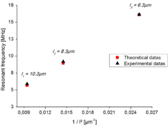
The dynamic characterization of the nanocantilevers is performed in two ways (external and internal actuation-sensing configurations). First, the mechanical integrity of the nanocantilevers is assessed by external piezoelectric actuation and optical sensing of the fundamental mode resonant frequency. Measurements are performed in a home-made fully-automated Fabry-Perot interferometer configuration, under vacuum and ambient temperature conditions. The fully automated option allows convenient characterization at the nanocantilevers level by using the 3D displacement of the chip bearing the nanodevices under the laser spot. The resonant frequency values are compared to theoretical datas issued from finite elements modeling of the nanocantilevers exact configuration, taking into account the specific geometry of the piezoelectric stack (see Figure 2).
The piezoelectric actuation at the nanodevice level is then tested by biasing the top and bottom electrodes as shown in the scheme (see Figure 1). In a first attempt to check the piezoelectric actuation efficiency, no electrical poling of the PZT layer is performed. The results are shown in Figure 3 demonstrating that the piezoelectric layer acts as expected and does not necessarily require electrical poling prior to its use. Nevertheless, in a second attempt, PZT layer is poled at five times the coercitive field value (6.7kV/m) during 15 minutes and the resonant frequency peak shape successively measured shows the enhancement of the actuation efficiency by an increase of the amplitude value of around 30%.
Proceedings of 2013 Nanomechanical Sensing Workshop D. Dezest, F. Mathieu et al. Stanford University, Stanford, CA
In conclusion, we achieved integration of piezoelectric actuation capabilities on NEMS at the full wafer scale. Further work on the piezoelectric sensing demonstration by collecting the electrical charges generated by the PZT layer using a charge amplifier set-up is currently under progress. This work paves promising ways for NEMS to be used in configurations where transduction capabilities are integrated at the nanodevice level providing fabrication at the wafer-scale.
Figure 1: SEM image (false colors) of an array of four nanocantilevers showing the biasing scheme for the internal piezoelectric actuation. The cantilevers dimensions are 2µm wide and respectively 10.2, 8.2, 6.2 and 4.2µm long (scale bar corresponds to 20µm). The stack is composed of a 150nm thick PZT layer (green) sandwiched between a 100nm thick LNO lower electrode (brown) and a 12-120nm thick Ti-Pt upper electrode (blue). A 30nm thick thermal oxide (purple) grown on top of the silicon ensures the electrical insulation between the stack and the substrate. The structures are actuated by applying an AC voltage between the electrodes through a 100-700 nm thick Ti-Au metallization (yellow). The inset is a close view of the 10.2 µm long cantilever showing the different layers (scale bar corresponds to 3µm).
Figure 2: Plot of the fundamental mode resonant frequencies of 2.4µm wide cantilevers with three different lengths l showing the linear dependence on 1 / l². Theoretical datas (red) are obtained from finite element modeling. Experimental datas are obtained under external actuation and sensing configuration at
room temperature and under secondary vacuum (1,8.10-6 mbars).
Figure 3: Fundamental mode resonant frequency of a 2µm wide and 10.2µm long cantilever before (black curve) and after (red curve) poling of the PZT thin film. Measurements are achieved according to the integrated actuation (12.6mV AC voltage is applied) and external sensing configuration, at room temperature and under secondary vacuum (9.8.10-7 mbars). Each datas curve has been averaged 10 times. The structure exhibits a quality factor of 1150 at 9.63MHz.
REFERENCES:
[1] L. G. Villanueva, R. B. Karabalin, M. H. Matheny, E. Kenig, M. C. Cross, M. L. Roukes, “A Nanoscale Parametric Feedback Amplifier”, Nano Letters, vol. 11, pp. 5054-5059, 2011.
[2] M. Li, H. X. Tang, M. L. Roukes, “Ultra-Sensitive NEMS-based Cantilevers for Sensing, Scanned Probe and Very High-Frequency Applications”, Nat. Nanotechnol., vol. 2, pp. 114-120, 2007.
[3] Q. P. Unterreithmeier, E. M. Weig, J. P. Kotthaus, “Universal Transduction Scheme for Nanomechanical Systems Based on Dielectric Forces”, Nature, vol. 458, pp. 1001-1004, 2009.
[4] J. Arcamone, M. A. F. van den Boogaart, F. Serra-Graells, J. Fraxedas, J. Brugger, F. Perez-Murano, “Full-Wafer Fabrication by Nanotencil Lithography of Micro/Nanomechanical Mass Sensors Monolithically Integrated with CMOS”, Nanotechnology, vol. 19, 305302, 2008.
[5] I. Bargatin, E. B. Meyers, J. S. Aldridge, C. Marcoux et al., “Large-Scale integration of NEMS for Gas Sensing Applications”, Nano Letters, vol. 12, pp. 1269-1274, 2012. [6] S. Guillon, D. Saya, L. Mazenq, J. Costecalde, D. Remiens,
C. Soyer, L. Nicu, “Lead Zirconate Titanate Nanoscale Patterning by UV-based Lithography Lift-Off Technique for Nano-Electromechanical Systems Applications”, IEEE Trans. On Ultrasonics Ferroelec. Freq. Control, vol. 59, pp. 1955-1961, 2012.