Fabrication, Morphological And Optoelectronicproperties Of Antimony On Porous Silicon As Msm Photodetector
12
0
0
Texte intégral
(2) H. A. Hadi. J Fundam Appl Sci. 2014, 6(2), 175-186. 176. These characteristics make it a suitable material for use in photodetectors[2].The basic idea of metal-semiconductor-metal photodetector based porous silicon is to reduce the light reflection in order to enhance the light sensitivity and on the other hand to enhance the effects of the electrical carries generated in the porous regions[3].To increase the sensitivity of metal/PS/cSi structures in the short-wavelength region, the PS layer must be made transparent (thin, highly porous or oxidized) [4]. The quantum efficiency is the number of electron-hole pairs generated per incident photon. A related figure of merit is the responsivity, which is the ratio of the photocurrent to the optical power. Therefore, for a given quantum efficiency, the responsivity increases linearly with wavelength [5]. The spectral dependence of photoconduction signal was measured in two geometries: The first one by measuring the photo-resistance of PS layer between parallel linear contacts on from PS surface. The second by measuring the photoresistance between the linear contacts (from the PS surface) connected in parallel and the backside contact of silicon wafer on which was obtained PS layer [6].OCVD method is one of the most widespread methods for determining carrier lifetime in bulk of diode structures. When forward current flows through diode, circuit is abruptly open and forward voltage drop decay is measured. For particular case of a thick diode structure with a homogeneous base and abrupt PN junction, carrier life time can be determined from slope of voltage decay [7] by using the following relation: τ=m. KT dV ( ) q dt. (1). Where conditions, 1 ≤ m ≤ 2 m = 1 describes low injection m = 2 should be used under high. injection conditions), k is Boltzmann constant, T absolute temperature and q elementary charge. This approximation expresses the so-called ‘‘OCVD carrier lifetime’’. Generally, exact solution can be obtained by solving continuity equation (it may be non-linear). Voltage decay may also depend on other parameters, such as diode base width junction capacitance and parallel resistance. The former allows us to determine highest level life time sHL (Carrier high injection), while latter permits us to extract low level life time sLL (Carrier low injection) [8]. This Paper explains precisely silicon substrate preparation, procedure of making porous on silicon substrate and characterization of porous silicon as well as the Sb/PS/n-Si/Al device. We use n-type silicon (111) orientation with resistivity 5−10Ω.cm. The structure of the porous silicon (PS) was investigated using x-ray diffraction, optical microscopy, and Atomic Force Microscopy. Also, photocurrent for different light power densities from illuminations I-V characteristics was discussed. The main goal in this work, to estimate optoelectronic properties.
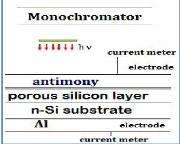
(3) H. A. Hadi. J Fundam Appl Sci. 2014, 6(2), 175-186. 177. such as responsivity, quantum efficiency and carrier life time of Sb/PS/n-Si heterojunction at 20mA/cm etching current density and etching time of 10 min.. 2. EXPERIMENTAL 2.1. Preparation of porous silicon: The wafer used was n-type Si (111) with a resistivity of 5−10Ω.cm Sample was etched by using mixture of 40 % HF: 99.9 % Methanol (1:1) for 10 min with current density of 20 mA/cm subjected to external illumination with a 30 mW diode laser 650 nm. %. The obtained porous silicon layer has a porosity value of about 70%. The thickness of the PS film was 88 nm determined using gravimetric method .After photo electrochemical etching, sample was cleaned with methanol and distilled water. Metallization on PS also became another important area of interest, especially in Schottky diode structure. Success of PS in application areas depended on how challenges in seeking suitable metallization could be overcome [9]. Here ohmic contacts on both PS and bulk silicon were made by deposition of high purity Al films by using thermal resistive technique under vacuum pressure of 10 torr. After evaporation process, thickness of evaporated film on a glass substrate was measured using gravimetric method. The evaporation is performed in a vacuum pressure of 10. torr, using an. evaporation plant model “E306 A manufactured by Edwards high vacuum”.. 2.2. Measurement: The morphological properties of PS layer such as nanocrystalline size, the structure aspect of PS layer and lattice constant have been investigated in this work by using X-ray device (shimadzu - XRD6000) supplied from Shimadzu Company /Japan. The source of X-ray radiation has been Cu-Kα radiation with 0.15406 nm wavelength. The device has been operated at 40 KV and 30 mA emission current. The sample is scanned from (20 - 50 degrees) 2Theta.In this work, an AA 3000 Scanning Probe Microscope AFM system has been used. The root mean square of roughness and grain size are obtained by using certain software. Dark current–voltage measurements in forward and reverse directions of Sb/PS/c-Si/Al heterojunction were carried out. Measurements of photocurrent of heterojunction were done under white light of different illumination power densities (with 0.75cm2 active area ) supplied by a halogen lamp with power of 150 W, which was connected to a Variac and calibrated by power meter. The photosensitivity of the photodetector was investigated in the wavelength range of 400-1000 nm with the aid of Joban-Yvon monochromatic and standard Si power meter as shown in Fig.1..
(4) H. A. Hadi. J Fundam Appl Sci. 2014, 6(2), 175-186. 178. Fig.1. Schematic setup of spectral photo responsivity measurement. Open circuit voltage (Voc) of heterojunction was investigated as function of light power. Life time measurement of photovoltaic porous devices was measured using OCVD technique. For this measurement a stroboscope and storage CRO (Philips 100 MHZ) were used. This magnitude could be determined from slope of voltage decay ∆V/∆t using Eq. (1). A steady-state excess carrier concentration was applied by a forward current flow through a diode. After an. abrupt opening of the circuit at t = 0, recombination of excess carriers would take place and the diode’s open voltage was monitored as shown in figure 2. Initial voltage step at t = 0 was due to voltage drop in diode, which was observed when the current flow stopped [10].. Fig.2. Variation of voltage after opening the circuit (OCVD) method [7] 3. RESULT AND DISSECTION Figure 3 shows a typical peak diffraction pattern reflection from the porous silicon substrate a position 33° and the peak near 29° corresponding Si .The intensity of peak porous silicon PS. layer (porosity of 70% ) sample decreased dramatically to six times low compared to the peak of bulk silicon Si, and this peak becomes very broad with anodization current densities as shown.
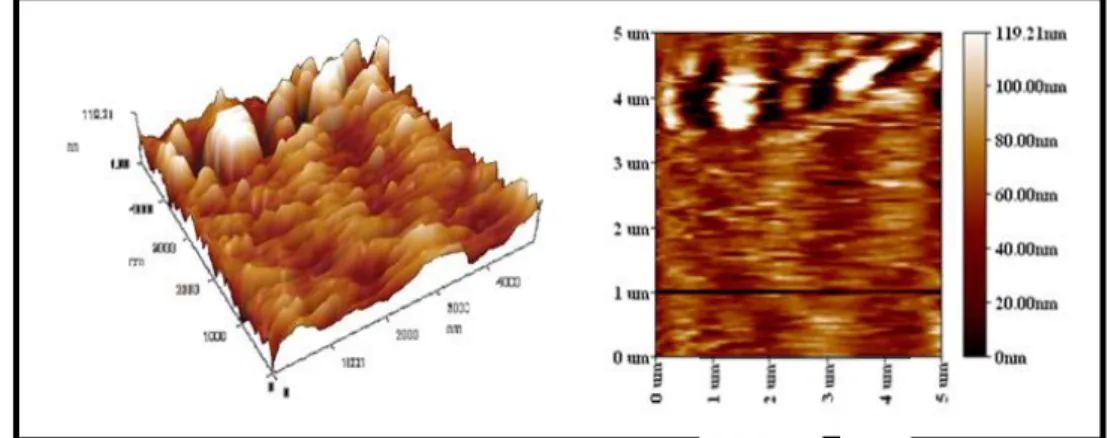
(5) H. A. Hadi. J Fundam Appl Sci. 2014, 6(2), 175-186. 179. in Fig.2.The X-ray diffraction pattern was confirmed the existence of nanostructure porous crystalline nature with grain size of 78nm was calculated by Scherer formula[11] : L=. Kλ ∆(2θ)COSθ. (2). Where λ is the wavelength of the X-rays, θ is the Bragg diffraction angle at the peak position in degrees, Δ(2θ) is the FWHM in radian, and k is a correction factor. The value of k is usually chosen to be 0.9 for Si films.. Fig.3. XRD patterns of the porous silicon layer at 20mA/cm2 etching current density for 10min etching time and the inset of figure 3 shows XRD patterns of bulk n-Si. The estimate of the porosity and thickness of the PS layers were made by gravimetric measurement and were of 70% and 88nm respectively. Figure 4 shows the surface roughness and pyramid like hillocks with un-uniform different heights surface. The scanning area used, is 5µm ×5µm and nano-crystalline silicon pillars and voids over the entire surface can be seen in. 3D AFM image in figure 4. The RMS surface roughness was 23.3nm. Sz( ten point height) was 119.7 nm and roughness average was 17.2 nm.from previous data and our results (irregular and randomly distributed), we can understand why structure of porous heterojunction is always nonuniformly distributed and the difference over large area may be considerable ..
(6) H. A. Hadi. J Fundam Appl Sci. 2014, 6(2), 175-186. Fig.4. 2D and 3D AFM images of PS surface at 20. /. 180. and 10min etching time.. Figure 5 shows the morphology of Sb surface and right inset show the optical micrograph of bulk silicon n-Si and PS surface formed at 20mA/cm etching current density for etching time of 10min. This confirms anodic dissolution of silicon surface leading to porous structure formation and variation of silicon surface colors indicates these surfaces are having different band gap. And hence give this figure indicates a significant variation in microstructure between the mirror-like silicon surface and porous surface as shown in Fig.3. The bulk Si has indirect band gap, but porous PS has direct and wide band gap due the quantum confinement.. Fig. 5. Optical micrograph of Sb/PS surface on n-Si at (M = 1,000), right inset show the optical micrograph of bulk silicon n-Si and PS surface formed at 20 mA/. etching current. density (M = 1,000). Figure 6 shows forward and reverse current–voltage characteristics of heterojunction measured under dark and illumination with different light power densities respectively. The junction exhibits good rectification ratio of 105 at bias of 2V. A large photocurrent to dark-current contrast ratio higher than 55 orders of magnitude and low dark currents below 0.89nA. The.
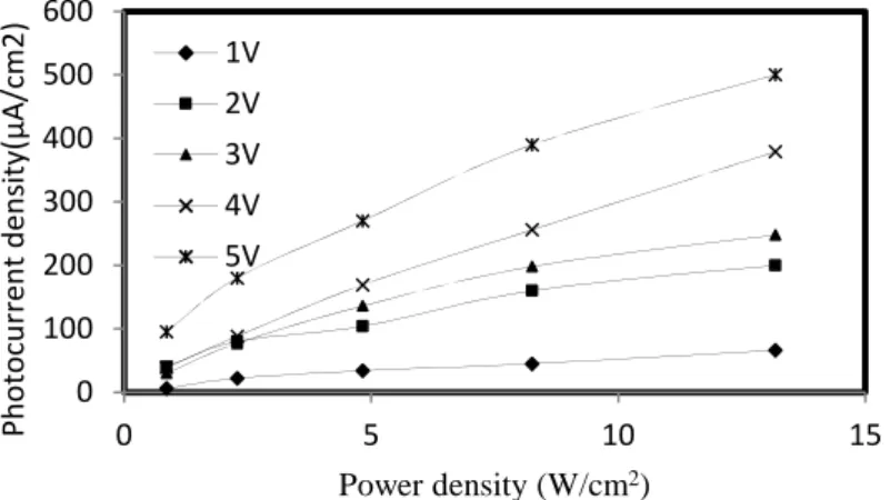
(7) H. A. Hadi. J Fundam Appl Sci. 2014, 6(2), 175-186. 181. photocurrent is measured for light power densities of 0.85–13.17 W/cm2. The current starting at a low voltage corresponds to that of a typical thermionic emission. In linear region, thermionic emission and carrier velocity increases. When light power density is increased, the photocurrent is increases due to generation of electron– hole pairs. No soft breakdown has been noticed in the prepared heterojunction at rang of voltage was used. These results are in good agreement with those reported earlier [12]. The current reaches a saturation value at higher bias voltage > −2 , the electric field is strong enough to separate any generated pair for certain incident power.. Fig.6. Dark current and photocurrent as a function of bias voltage measured at room temperature for a PS/n-Si MSM photodetector with 0.75. active area. The photocurrent is. measured under halogen lamp illumination with different power density The photovoltaic effect is observed and the photocurrent increase with power density and bias dependence. From Fig.7, it observed that these heterojunction have good linearity characteristics. Figure 8 shows relation between open-circuit voltage (Voc) with incident photon power of halogen lamp for n-type heterojunction and the Open circuit voltage V is 159 mv and saturation occurs after power density 2.28 mW/cm2..
(8) J Fundam Appl Sci. 2014, 6(2), 175-186. Photocurrent density(μA/cm2). H. A. Hadi 600. 182. 1V. 500. 2V. 400. 3V. 300. 4V. 200. 5V. 100 0. 0. 5. 10. 15. Power density (W/cm2). Voc(mV). Fig.7. linearity of photodetector device as a function of incident photo energy density 180 160 140 120 100 80 60 40 20 0. 0. 3. 6. 9. 12 15 18 21 24 27 30 33 36 power density (W/cm2). Fig.8. Open circuit voltage as a function of the incident photo energy density Figure 9 shows the spectral responsivity of Sb/PS/n-Si device under white illumination the higher light sensitivity (0.225A/W) is observed at shorter wavelength 400 nm than visible region 700nm which has of (0.15A/W) , because of the incident energy is higher than the excitation energy of electron-hole pairs and that mean , the wavelength in near UV region is absorbed in the depletion region of Sb/PS contact .The lower light sensitivity peak (0.15W/A) is a result of absorption of 700 nm in the depletion region of PS/n-Si heterojunction interface. The quantum confinement effects interpret this result.The direct band gab semiconductor offer much stronger absorption coefficient; therefore, the porous silicon has better optoelectronic properties than bulk silicon..
(9) H. A. Hadi. J Fundam Appl Sci. 2014, 6(2), 175-186. 183. 0,25. Responsivity (A/W). 0,2. 0,15. 0,1. 0,05. 0. 0. 200. 400. 600. 800. 1000. 1200. Wavelength(nm). Fig.9. Responsivity as a function of various incident wavelengths for Sb/ PS/n-Si PD The quantum efficiency is related with responsivity by the relation . . = 1245. (3). Figure 10 shows the variation of quantum efficiency as function of wave length for Sb/PS/nsi .device two peaks are showing in the Figure 6, the first one of 0.70% at 400nm and the second was 0.26% at 700nm.The high of Q.E. in near UV-visible region indicate that increasing the light sensitivity and reduced the light reflected in the porous regions at both sides of device structure, the first one Sb/PS and other in PS/n-Si respectively .A different sensitivity of quantum efficiency were reflected the effects of the electrical carries generated in the porous regions . 0,8. Quantum effecincy. 0,7 0,6 0,5 0,4 0,3 0,2 0,1. 0. 0. 200. 400. 600. 800. Wavelength(nm). 1000. 1200. Fig.10. Quantum efficiency as a function of various incident wavelengths for Sb/PS/n-Si PD.
(10) H. A. Hadi. J Fundam Appl Sci. 2014, 6(2), 175-186. 184. The lifetime are evaluated using OCVD method and the carrier life time is 100 μs, OCVD shapes for prepared heterojunctions are shown in Fig. 11 Life time values obtained by using Eq. (1) under a condition of intermediate injection, where excess minority carrier concentration in base is higher than thermal-equilibrium minority carrier concentration but less than thermal equilibrium majority carrier concentration. These values are higher than those reported earlier [13]. Life time dependence on Voc is exponential in broad terms [14]. It has been found that the carrier life time in the structure of porous heterojunction is always non-uniformly distributed and the difference over large area may be considerable. Thus, this study confirms that OCVD method is very sensitive to structural defects [7]. Experimental results reveal that recombination center sites are produced either inside the bulk (n-Si substrate) or at surface/interface depending on heterojunction preparation conditions.. Fig. 11. Photo-Induced Open-Circuit Voltage Decay Photograph for 20 mA/cm 2etching current density at 10min etching time (τ = 100 μs, Hor.50 μs/div, Ver.10 mV/div) The excess carriers’ life time measured by OCVD provides a carrier effective life time bulk life time τ. depending on τ. bulk and surface life time. as shown in the following. equation [15]: τ. 1. =. τ. 1. +. 1. (4). Accuracy of OCVD measurement depends on precession of oscilloscope, temperature measurement and noise. The total error of estimated lifetime is lower than 10 %. The diode works in on-state under a resistive load with a small parasitic inductance in series. With a sudden stop of current flow using fast external semiconductor switch, leaving the diode in an open circuit and forcing excess carrier removal by internal recombination and diffusion processes. This is electrically manifested on time decay of diode voltage drop, in which two linear slopes that correspond to the conditions of high or low injection are observed [8]..
(11) H. A. Hadi. J Fundam Appl Sci. 2014, 6(2), 175-186. 185. 4. CONCLUSION In conclusion, we fabricated and characterized MSM photodetector .Experimental results reveal that recombination center sites are produced either inside the n-Si or at surface PS/n-Si interface depending on structural and morphological properties. Dark and illumination current-voltage (I-V) measurements of the Sb/PS-based MSM photodetector are studied. Figure of merits of Sb/PS/n-Si/Al device at near UV and visible will be conducted to illustrate their potential application in photonics. The photodetector device based in porous layer PS will become more efficient than the normal n-Si silicon substrate. The results show that Sb on porous silicon PS structures will act as good candidates for making highly efficient photodiodes.. 5. REFERENCES [1] Chou C.M. Cho H.T., Hsiao V.K.S., Yong K.T. and Law W.C., Nanoscale Research Letters 2012, 7(1):291, (1-4). [2] Abd Rahim A.F., Hashim M.R., Ali N.K. and Yusuf R., IEEE Xplore Digital Library.2012 pp.1-2. International Conference on Enabling Science and Nanotechnology (ESciNano 2012) 5-7 January 2012, Persada Johor International Convention Center, Johor Bahru,MALAYSIA. [3] Sheng W.G., Hai L., Feng X., Jun C.D., Fang R.F., Rong Z. and Dou Z.Y.Chinese Physics Letters.2012,29(9),4.DOI: 10.1088/0256-307X/29/9/097302 [4] Balagurov L., Bayliss S., Yarkin D., Andrushin S., Kasatochkin V., Orlov A., and Petrova E., Solid-State Electronics.2003,47,65–69. [5] Sze S. and Kwok K., Physics of Semiconductor Devices, Third Edition Published by John Wiley & Sons, Inc., Hoboken, New Jersey. Published simultaneously in Canada. (2007)614618. [6] A. Dafinei , G. Craciun, C. Flueram, C. Sargentis, and E. Niculescu" A photoconduction study on porous silicon” ,Authorized licensed use limited to: Iraq Virtual Science Library. Downloaded on September 26, 2011 UTC from IEEE Xplore. [7] Benda V.and Novak Z .Ser. Elec. Energ. 2002, 15, 33-39. [8] Gxasheka A.R. On the optical characterization of photovoltaic devices, PhD Thesis (Nelson Mandela Metropolitan University) (2008). [9] Siemieniec R., Scudkamp W., and Lutz J.Sol. Sta. Elect. 2002, 46, 891. [10]Uhlir A. and Uhlir I. Phys. Stat. Sol. 2005, 2(9) 3185-3187. [11] Bisi O., Ossicini S. and Pavesi L. Surface Science Reports. 2000,381-126. [12] Ismail R.e-J. Surf.Sci. Nanotechnology. 2010, 8, 383-391..
(12) H. A. Hadi. J Fundam Appl Sci. 2014, 6(2), 175-186. 186. [13] Nansheng Z., Zhongquan M., Chengyue Z. and Bo H.J. Journal of Semiconductors. 2009, 30 (7), 072004-1-072004-4. [14] Perpin˜a X., Jorda` X, Vellvehi M., Vobecky J. and Mestresc N.J. Electrochem. Soc. 2010, 157(7), H711-H720. [15] Ismail R., Al-Samare E. and Sultan A. Qatar. Univ. Sci. 2005, 25, 31-36.. How to cite this article: Hadi H A. Fabrication, morphological and optoelectronic properties of antimony on porous silicon as msm photodetector. J Fundam Appl Sci. 2014, 6(2), 175-186..
(13)
Figure

+2

Documents relatifs
fluorescence spectrum of a porous silicon sample obtained by etching in 1% [HMIM][BF4] w-IL system at a current density of 8 mA/cm2 for 6 hours Fig.. A more detailed study of
In our study we have developed a calculation model based on the combination of effective media approximations and transfer matrix method, which could precisely predict the
As shown in Figure 1b and S2, the surfaces after PEE comprised a 60 mm-thick porous layer composed of ~50 mm-thick straight macropores aligned in the [100] direction and spaced by
the vaporization zone which is lower in our experiments. With some modifications of the small.. 4 Raman spectra: a) porous silicon obtained by vaporization with solar furnace;
We observe a nearly constant absorption from room temperature down to cryogenic temperatures for two silicon samples pre- senting an optical absorption of 0.029 cm −1 and 780 ppm cm
On the contrary, in those conditions where the oxidation reaction (a) is the rate-limiting-step (e.g., etching of polished wafers in HF rich solutions), the sample or
In this chapter, the basic principles and considerations regarding thermoelectrics were discussed. Each thermoelectric effect was presented, while the possible
The interpretation of diagrams Stabler, Piper, Schoeller-Berkaloff and Stiff showed that groundwater in the region of Sidi Bel Abbes are characterized by a dominance of chloride,
