Raman study of
outgassing and damage induced by ion implantation in
-doped
D. Barba, V. Aimez, J. Beauvais, J. Beerens, D. Drouin, M. Chicoine, and F. Schiettekatte
Citation: Journal of Applied Physics 96, 4890 (2004); doi: 10.1063/1.1803615 View online: http://dx.doi.org/10.1063/1.1803615
View Table of Contents: http://aip.scitation.org/toc/jap/96/9
Published by the American Institute of Physics
Articles you may be interested in
Concepts for particle foam based ultralight automotive interior parts
AIP Conference Proceedings 1593, 354 (2015); 10.1063/1.4873799
MUSIC imaging method for electromagnetic inspection of composite multi-layers
AIP Conference Proceedings 1650, 453 (2015); 10.1063/1.4914641
Novel insight into the hydrogen absorption mechanism at the Pd(110) surface
The Journal of Chemical Physics 140, 134705 (2014); 10.1063/1.4869544
Laser polishing of additive laser manufacturing surfaces
Journal of Laser Applications 27, S29102 (2015); 10.2351/1.4906385
Effect of heat treatments and coatings on the outgassing rate of stainless steel chambers
Journal of Vacuum Science & Technology A: Vacuum, Surfaces, and Films 32, 021604 (2013); 10.1116/1.4853795
Hydrogen traps in the outgassing model of a stainless steel vacuum chamber
Journal of Vacuum Science & Technology A: Vacuum, Surfaces, and Films 32, 031604 (2014); 10.1116/1.4869962
Raman study of As outgassing and damage induced by ion implantation
in Zn-doped GaAs
D. Barba,a)V. Aimez, J. Beauvais, J. Beerens, and D. Drouin
Département de Génie Électrique et de Génie Informatique, Université de Sherbrooke, Sherbrooke, Quebec J1K 2R1, Canada
M. Chicoine and F. Schiettekatte
Département de Physique, Université de Montréal, Montréal, Quebec H3C 3J7, Canada (Received 19 April 2004; accepted 7 August 2004)
Room temperature micro-Raman investigations of LO phonon and LO phonon-plasmon coupling is used to study the As outgassing mechanism and the disordering effects induced by ion implantation in Zn-doped GaAs with nominal doping level p = 7⫻1018 cm−3. The relative intensity of these two peaks is measured right after rapid vacuum thermal annealings(RVTA) between 200 and 450 °C, or after ion implantations carried out at energies of 40 keV with P+, and at 90 and 170 keV with As+. These intensities provide information regarding the Schottky barrier formation near the sample surface. Namely, the Raman signature of the depletion layer formation resulting from As desorption is clearly observed in samples submitted to RVTA above 300 ° C, and the depletion layer depths measured in ion implanted GaAs: Zn are consistent with the damage profiles obtained through Monte Carlo simulations. Ion channeling effects, maximized for a tilt angle set to 45° during implantation, are also investigated. These results show that the Raman spectroscopy is a versatile tool to study the defects induced by postgrowth processes in multilayered heterostructures, with probing range of about 100 nm in GaAs-based materials. © 2004 American Institute of Physics.
[DOI: 10.1063/1.1803615]
I. INTRODUCTION
Raman spectroscopy is a powerful nondestructive tech-nique used to study the variation of crystallinity in III-V semiconductors after rapid thermal annealing,1,2 recrystalliz-ing processes,3 ion beam etching,4 and ion implantation.5,6 Many Raman scattering measurements performed in n- and
p-type materials have put the emphasis on the longitudinal
vibration of the carrier plasma which couples with the LO phonon via the macroscopic electric field to form a phonon-like LO phonon-plasmon coupling (LOPC) mode. Such a mechanism has been studied in p-type GaAs as a function of different carbon,7 silicon,8 beryllium,9,10 and zinc11 doping levels. These previous reports have shown that the relative integrated areas of the LO phonon bands共ILO兲 and the LOPC bands 共ILOPC兲 can directly be connected to the free carrier concentration located in the Raman probed volume, thus al-lowing one to estimate the depletion layer depth in the vicin-ity of the sample surface.
In this paper, we present micro-Raman investigation of
p = 7⫻1018cm−3 Zn-doped 共100兲 GaAs substrates after rapid vacuum thermal annealings (RVTA) or after ion im-plantations. We show that this experimental technique can provide both quantitative and qualitative information regard-ing the defects induced by these two postgrowth processes. The measurements of the ILO/ ILOPC ratio between 200 and 400 cm−1are obtained with the help of the data reported by Irmer et al. for heavily doped p-type GaAs with low carrier mobility.11 Our results enable us to study the mechanisms
involved in the Schottky barrier formation, and to measure the range of the damage these mechanisms generate near the sample surface. First, the evolution of the depletion layer depth observed in RVTA-processed samples is analyzed in terms of surface reconstruction and desorption effects.12,13 Second, we investigate unannealed P+ and As+ implanted
materials with different ion beam energies, where tilt angles were set to 7° and 45°, in order to minimize or to maximize the ion channeling, respectively. These measurements are fi-nally compared to the damage profile calculated usingSRIM 2003 Monte Carlo simulations.14
II. EXPERIMENTS
The RVTA of unimplanted samples were performed dur-ing 60 s at 10 mbar, with annealdur-ing temperatures varydur-ing between 200 and 400 ° C. Ion implantations have been car-ried out at T = 20 ° C using a Tandetron accelerator. P+were implanted with ion beam energies of 40 keV, and As+ions were implanted into GaAs: Zn with incident energies of 90 and 170 keV. For each of these implantations, the tilt angles were set at 7° and 45° with a precision of ±2°. To avoid amorphization, which occurs at lower thresholds for this implant temperature,15 the fluences were restricted to 1013ions/ cm2 and 1012 ions/ cm2 for P+ and As+,
respec-tively.
One cm−1 resolution micro-Raman studies were carried
out at room temperature in the z共xy兲z¯ backscattering geom-etry, using a LABRAM-800 confocal system equipped with a nitrogen-cooled charge-coupled device detector and a 50⫻ microscope lens. A 514.5 nm Ar laser line focused on a diameter spot of few microns and polarized perpendicular to a)Electronic mail: [email protected]
the具100典 growth axis of the samples was used for excitation. The laser power was kept at 30 mW to prevent sample heat-ing.
III. RESULTS AND DISCUSSION A. Raman analysis
Since GaAs belongs to the point group of symmetry Td, only the LO phonon and the LOPC excitation are dipole allowed in the z共xy兲z¯ optical configuration. The depths ex-plored by the Raman probe are 60 nm for confocal hole di-ameter h = 0.5 mm, and of⬇100 nm for h=1.0 mm.16,17
Our estimation of the depletion layer depth is based on the Schottky model, assuming that the carrier concentration abruptly rises to the bulk value at a distance d away from the sample surface. According to Ref. 11, this value can be de-duced from Raman measurements using the relation
d =␦
2ln
冉
1 +A A0
冊
, 共1兲
where ␦ corresponds to the penetration depth of the laser light with wavelength =514.5 nm, extracted from Ref. 16,
A is the measured ratio of the peak integrated intensity
ILO/ ILOPC, and A0 refers to the ILO/ ILOPCareas ratio calcu-lated in pure GaAs, given in Ref. 11.
B. Vacuum thermal annealed GaAs: Zn
Figure 1 shows the Raman spectra between 240 and 310 cm−1of unimplanted GaAs: Zn, for an unannealed
refer-ence sample and for samples annealed at 250, 300, 350, and 400 ° C. This set of measurements was obtained by using h = 1 mm, in order to probe the effects induced by RVTA in the first 100 nm of the materials. The dotted lines denote the fitted forbidden TO and allowed LO phonons bands, ob-served at 269 and 290 cm−1, respectively. The dashed lines
identify the LOPC mode, with energy ranging
270– 274 cm−1, and the solid lines refer to the sum of TO
phonon, LO phonon, and LOPC bands. The corresponding ILO/ ILOPCratios and depletion depths are estimated using Eq.
(1) and reported as a function of the annealing temperature in
Fig. 2.
The observation of Raman signal at the TO frequency is associated with disorder effects resulting from Zn doping and so-called forbidden TO-phonon scattering.18 The measured wave numbers and bandwidths of TO phonon, LO phonon, and LOPC bands are close to those reported by Irmer et al.11 in p = 7.2⫻1018cm−3 GaAs: Zn. The constant energy
posi-tion of the TO phonon and LO phonon lines indicates low contamination effects resulting from RVTA. On the other hand the LOPC energy softening observed in the samples annealed above 300° C denotes a significant reduction of the carrier mobility in these materials due to the generation of defects within the structure.11
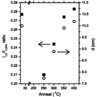
The vacuum heating of GaAs leads to surface recon-struction and outgassing effects, which promote the forma-tion of extended defects in the vicinity of the sample surface. Such mechanisms have been studied by means of atomic force microscopy,12low-energy electron diffraction measure-ments, and Auger electron spectroscopy.13 These previous reports have allowed the authors to describe the surface re-construction processes induced by thermal annealings per-formed up to about 350 ° C, showing that the As atoms are displaced outward and the Ga atoms inward with respect to the bulk. Above T = 350 ° C, it has been established that both As and Ga atoms desorb from the substrate. However, this process favors the generation of As vacancies in the upper layers of the sample, due to the higher desorption rate of As with respect to Ga between 300 and 600 ° C.19This scenario is consistent with the data reported in Fig. 2. Indeed, the decrease of the depletion depths from 10 nm in unannealed sample to 7.8 nm in vacuum annealed samples at 250 ° C can FIG. 1. Raman signature of reference unannealed GaAs: Zn material(a) and
vacuum annealed samples during 60 s at T = 250 ° C(b), T=300 °C (c), T
= 350 ° C(d) and T=400 °C (e). The solid lines are the sum of the fitted
LOPC(dashed lines), TO phonon, and LO phonon (dots) bands. FIG. 2. Relative integrated area of the measured LO phonon and the LOPC mode共䊏兲 as a function of annealing temperature, with the corresponding depletion depth 共䊊兲 calculated from Eq. (1). The data associated with T = 20 ° C designate the unannealed material.
be connected to the displacement of the As donors toward the sample surface. On the other hand, the presence of As vacancies excess, resulting from preponderant As desorption during RVTA performed between 300 and 400 ° C, agrees with the increase of depletion depths from 7.6 to 10.2 nm in this temperature range(Fig. 2).
C. Ion implanted GaAs: Zn
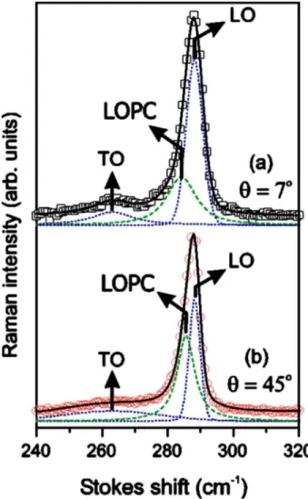
Figures 3 and 4 illustrate measurements obtained in the 240– 320 cm−1 spectral range using confocal hole h = 0.5 mm and Fig. 5 with h = 1.0 mm, so that most of the damage induced by the different ion implantations is located in the Raman probed volume. Figures 3(a) and 3(b) corre-spond to P+ implanted materials at 40 keV, with tilt angles
equal to 7°(a) and 45° (b), whereas Figs. 4(a) and 4(b) and Figs. 5(a) and 5(b) report on Raman spectra recorded in As+
implanted material at 90 and 170 keV, respectively. The solid line designates the fitted spectra, which includes the contribution of TO phonon band at 265 cm−1, LO phonon
band at 289 cm−1, and LOPC mode around 285 cm−1.
All these Raman spectra exhibit a drastic enhancement of the ILO/ ITOratio by a factor of up to 10 with respect to the unimplanted samples(Fig. 1). Such an increase is associated with impurity-induced Raman scattering,20and accompanied
by a LO phonon softening of 2 cm−1 resulting from ion
in-corporation within the structure. This energy shift is very close to the value reported by Ashokan et al.5 in P+ im-planted GaAs at 70 keV with fluence of 1013ions/ cm2.
The depletion depths deduced from the measured ILO/ ILOPCratios are reported in the third and fifth columns of Table I with a few nanometers accuracy. These experimental values compare well with the SRIM calculations, giving the average penetration depth Rp of implanted ions in GaAs for corresponding ion beam energy and tilt angle, in fourth and sixth columns of Table I. Although the SRIMsimulations do not include ion channeling effects,14which increase the lon-gitudinal path of implanted ions within the target,21 discrep-ancies of less than 8 nm are observed between measurements and calculations. We note that the depletion layer depths are slightly smaller than expected for the 45° implant angle, thus showing the negligible contribution of channeled ions to the experimental data. These remarks suggest that the formation of a large depletion layer below the sample surface is mainly connected to the range of defects arising from nuclear colli-sions between host atoms and incident ions, rather than to the spatial distribution of implanted ions. According to electrical conductivity measurements of Zn+, S+, and N+ implanted
GaAs,22such a feature is due to the trapping of free carriers by atoms displaced from their original site. We conjecture FIG. 3. Room temperature Raman spectra of P+implanted GaAs: Zn at
40 keV with tilt angles set to 7°(a) and 45° (b).
FIG. 4. Room temperature Raman spectra of As+implanted GaAs: Zn at 90 keV with tilt angles set to 7°(a) and 45° (b).
that this type of defect affects the LOPC mechanism by modifying the local electron gas density.
Finally, in Figs. 3(b), 4(b), and 5(b) the LOPC modes are observed at 289, 287, and 289 cm−1, whereas they appear at
285, 284, and 288 cm−1in Figs. 3(a), 4(a), and 5(a),
respec-tively. According to Ref. 11, such a spectral shift reveals higher carrier mobility in GaAs: Zn samples implanted at = 45°. In agreement with the previous analysis, this result is attributed to lower crystal damage in the Raman probed vol-ume, associated with nuclear cross-section lowering and ion channeling effects.21
IV. CONCLUSION
Raman experiments carried out in the 240– 320 cm−1
spectral range were used to investigate the defects generated by As outgassing in vacuum thermal annealed p-type GaAs: Zn between 250 and 450 ° C. We have shown that the measurements of depletion layer depths agree with the ex-pected changes of local free carrier density resulting from As atom displacements and desorption during RVTA.
We have also studied the crystal disorder associated with P+ and As+ implantations performed at different ion beam energies and tilt angles in p = 7⫻1018 cm−3 GaAs: Zn. The spectral signature of LO phonon and LOPC mode have al-lowed us to probe the damaged layers located up to 90 nm within the substrate. Our results make the Raman technique a simple and accurate technique to measure the range of de-fects induced by nuclear collisions during low-energy ion implantation.
ACKNOWLEDGMENT
The authors acknowledge financial support from Nano-Québec for this work.
1
J. Wagner, M. Peter, K. Winkler, and K. H. Bachem, J. Appl. Phys. 83, 4299(1998).
2
A. Saher Helmy, A. C. Bryce, C. N. Ironside, J. S. Aichison, and J. H. Marsh, Appl. Phys. Lett. 74, 3978(1999).
3
K. Mizoguchi, S. Nakashima, Y. Sugiura, and H. Harima, J. Appl. Phys.
85, 6758(1999).
4
F. Frost, G. Lippold, A. Schindler, and F. Bigl, J. Appl. Phys. 85, 8378
(1999). 5
R. Ashokan, K. P. Jain, H. S. Mavi, and M. Balkanski, J. Appl. Phys. 60, 1985(1986).
6
K. Santhakumar, P. Jayavel, R. Kesavamoorthy, P. Magudapathy, K. G. M. Nair, and V. Ravinchandran, Nucl. Instrum. Methods Phys. Res. B 194, 451(2002).
7
M. Seon, M. Holtz, W. M. Duncan, and T. S. Kim, J. Appl. Phys. 85, 7224
(1999). 8
T. Kamijoh, A. Hashimoto, H. Takano, and M. Sakuta, J. Appl. Phys. 59, 2382(1986).
9
A. Mlayah, R. Carles, G. Landa, E. Bedel, and A. Muñoz-Yagüe, J. Appl. Phys. 69, 4064(1991).
10
R. Fukasawa and S. Perkowitz, Phys. Rev. B 50, 14119(1994). 11
G. Irmer, M. Wentzel, and J. Monecke, Phys. Rev. B 56, 9524(1997). 12
A. Guillén-Cervantes, Z. Rivera-Alvarez, M. López, E. López-Luna, and I. Hernàndez-Calderón, Thin Solid Films 373, 159(2000). 13
F. Proix, A. Akremi, and Z. T. Zhong, J. Phys. C 16, 5449(1983). 14
J. F. Ziegler, J. P. Biersack, and U. Littmark, The Stopping and Ion Range
of Ions in Matter(Pergamon, New York, 1985). 15
E. Wendler, B. Breeger, C. Schubert, and W. Wesch, Nucl. Instrum. Meth-ods Phys. Res. B 147, 155(1999).
16
D. E. Aspnes and A. A. Studna, Phys. Rev. B 27, 985(1983). 17
J. S. Blakemore, J. Appl. Phys. 53, R123(1982). 18
D. Olego and M. Cardona, Phys. Rev. B 24, 7217(1981). 19
T. E. Haynes, W. K. Chu, T. L. Aselage, and S. T. Picraux, J. Appl. Phys.
63, 1168(1988).
20
C. Trallero-Giner, A. Cantarero, M. Cardona, and M. Mora, Phys. Rev. B
45, 6601(1992).
21
P. D. Townsend, J. C. Kelly, and N. E. W. Hartley, Ion Implantation,
Sputtering and their Applications(Academic Press, London, 1976), p. 45.
22
Y. Kato, T. Shimada, Y. Shiraki, and K. F. Komatsubara, J. Appl. Phys. 45, 1044(1974).
FIG. 5. Room temperature Raman spectra of As+implanted GaAs: Zn at 170 keV with ion beam oriented at 7°(a) and 45° (b) with respect to the
surface normal.
TABLE I. Depletion layer depths deduced from the measured ILO/ ILOPC areas ratios in ion implanted GaAs: Zn with tilt angles set to 7° and 45°, and projected range of implanted ion calculated usingSRIM2003 simulations.
Implantation = 7° = 45°
Ion Energy(keV) d共nm兲 Rp共nm兲 d共nm兲 Rp共nm兲
P 40 44 37 28 30
As 90 40 39 21 29
170 74 69 44 52