HAL Id: hal-03137414
https://hal-univ-rennes1.archives-ouvertes.fr/hal-03137414
Submitted on 15 Feb 2021
HAL is a multi-disciplinary open access
archive for the deposit and dissemination of
sci-entific research documents, whether they are
pub-lished or not. The documents may come from
teaching and research institutions in France or
abroad, or from public or private research centers.
L’archive ouverte pluridisciplinaire HAL, est
destinée au dépôt et à la diffusion de documents
scientifiques de niveau recherche, publiés ou non,
émanant des établissements d’enseignement et de
recherche français ou étrangers, des laboratoires
publics ou privés.
Okan Yurduseven, Choonsup Lee, David González-Ovejero, Mauro Ettorre,
Ronan Sauleau, Goutam Chattopadhyay, Vincent Fusco, Nacer Chahat
To cite this version:
Okan Yurduseven, Choonsup Lee, David González-Ovejero, Mauro Ettorre, Ronan Sauleau, et
al..
Multi-Beam Si/GaAs Holographic Metasurface Antenna at W-Band.
IEEE Transactions
on Antennas and Propagation, Institute of Electrical and Electronics Engineers, 2020, pp.1-1.
�10.1109/TAP.2020.3030898�. �hal-03137414�
ACCEPTED MANUSCRIPT
Abstract—We demonstrate a silicon (Si) – gallium arsenide
(GaAs) semiconductor based holographic metasurface antenna operating at 94 GHz. The metasurface antenna molds the radiated beam by resorting to a holographic approach involving the modulation of a guided-mode generated by a pillbox beam former. The pillbox beam former is fed by three integrated horns in Substrate Integrated Waveguide (SIW) technology located in the focal plane of the parabolic reflector of the pillbox beam former. The three horns correspond to three independent beams and allow beam steering by switching from one feed to another. The proposed metasurface antenna is planar and extremely low-profile, thus suitable for small platforms such as CubeSats/SmallSats. A prototype validates the concept demonstrating a directivity as high as 31.9 dBi and a reflection coefficient lower than -15 dB at 94 GHz.
Index Terms—Metamaterial, metasurface, antenna,
millimeter-wave, beam shaping, silicon, gallium arsenide, holography.
I. INTRODUCTION
metasurface antenna is a planar aperture synthesized using an array of sub-wavelength elements (or meta-atoms) [1]-[3]. Metasurfaces enable to control at will the aperture field distribution, in phase and amplitude, of a radiating structure. Conventional techniques to synthesize a desired radiation pattern in the antenna far field mostly rely on variants of the phased array concept [4], [5]. A phased array aperture is synthesized using an array of individual antenna elements, typically spaced at the Nyquist limit. Conventionally, each antenna element within a phased array exhibits a full phase control, enabled by a lossy phase shifter, and a power amplifier unit to compensate for the insertion loss. As a result, a phased array often exhibits a complex architecture and suffers from a high power consumption, especially as its electrical size grows. The concept of holography has been a trendsetter in optics, with applications ranging from interferometry to microscopy and data storage [6], [7]. In this context, holography can be considered as a synthesis technique, involving an objective function and a reference-wave. From their interference pattern, a grating can be calculated and the objective function may then
Submitted June 18, 2020; revised August 13, 2020; accepted October 04, 2020. This paper presents results of research carried out at the Jet Propulsion Laboratory, California Institute of Technology, under a contract with the National Aeronautics and Space Administration. It was funded under the Advanced Component Technology (ACT) Program. Corresponding author: O. Yurduseven.
O. Yurduseven and V. Fusco are with the Centre for Wireless Innovation, School of Electronics, Electrical Engineering and Computer Science, Queen’s University Belfast, BT3 9DT, Northern Ireland, UK (e-mail: okan.yurduseven@qub.ac.uk; v.fusco@ecit.qub.ac.uk).
be retrieved by exciting the recorded grating with the reference-wave. The application of holography at microwave and millimeter-wave frequencies has received considerable attention, particularly in the context of radar imaging and antenna measurements [8]-[11].
Building on these advances, the concept of holographic beam shaping metasurface antenna has recently gained significant traction [12]-[18]. Metasurface antennas have also been identified as good candidates for small platforms such as CubeSats/SmallSats where stowage volume is limited [19]. Similar to the well-known holography concept at optical frequencies, a holographic metasurface antenna achieves beam shaping by using the feeding source as the reference-wave and interacting it with the objective function (or the radiation pattern of interest). A significant advantage of the holographic beam shaping concept is that the synthesis of the desired aperture field distribution does not require phase-shifting circuits, simplifying the hardware architecture of the antenna. In this paper, we demonstrate a multi-beam holographic metasurface antenna micro-machined on semiconductor substrates and operating at 94 GHz. The proposed antenna enables three different radiation patterns on the same aperture, steered at 45° intervals in azimuth by switching between multiple coplanar waveguide (CPW) feeding ports. The design principle of the metasurface antenna relies on a discrete dipole principle [16], in which a sub-wavelength sampled grating (or metasurface) layer is derived by directly interacting the guided-mode reference-wave excitation with the objective function (desired aperture field distribution). The holographic discrete dipole principle eliminates the need for computationally expensive, time-consuming unit-cell based simulations to create an impedance database. The reference field exciting the metasurface is generated by a quasi-optical pillbox beam former [20], [21]. Such a quasi-optical system provides a planar wavefront and the required phase gradient for steering in the azimuthal plane. The contributions of this paper are as follows. First, the concept of holographic beam synthesis using a metasurface is realized by leveraging a semiconductor based enabling technology at millimeter-wave frequencies. We note that the radiation mechanism of the developed antenna in this
C. Lee, G. Chattopadhyay, and N. Chahat are with the Jet Propulsion Laboratory, California Institute of Technology, 4800 Oak Dr., Pasadena, CA 91109, USA (e-mail: choonsup.lee@jpl.hasa.gov; goutam.chattopadhyay@jpl.nasa.gov; nacer.e.chahat@jpl.nasa.gov).
D. Gonzalez-Ovejero, M. Ettorre, and R. Sauleau are with Univ. Rennes, CNRS, IETR (Institut d’Electronique et des Technologies du numéRique) – UMR 6164, F-35000 Rennes, France (email: david.gonzalez-ovejero@univ-rennes1.fr; mauro.ettorre@univ-david.gonzalez-ovejero@univ-rennes1.fr; ronan.sauleau@univ-rennes1.fr).
Multi-Beam Si/GaAs Holographic Metasurface Antenna at W-Band
Okan Yurduseven, Senior Member, IEEE, Choonsup Lee, David González-Ovejero, Senior Member,
IEEE, Mauro Ettorre, Senior Member, IEEE, Ronan Sauleau, Fellow, IEEE, Goutam Chattopadhyay,
Fellow, IEEE, Vincent Fusco, Fellow, IEEE, and Nacer Chahat, Senior Member, IEEE
ACCEPTED MANUSCRIPT
work, holographic metasurface, is fundamentally different from the conventional leaky-wave type radiation presented in [20] and [21]. Second, to the best of our knowledge, this is the first time that a holographic metasurface is designed to encode multiple radiation patterns, each activated by means of switching between the multiple input ports. Third, from the pillbox beamformer perspective, the presented substrate architecture consists of a dual-substrate material, Si and GaAs, with bonding required between these materials exhibiting different Coefficient of Thermal Expansion (CTE) characteristics, as opposed to the same type of material architecture for the multiple layers in [20] and [21]. Besides the technological aspects, the designed pillbox system overcomes the mismatch due to different dielectric constants, and at the same time, provides clean phase profiles for the wave illuminating the metasurface. Fourth, and finally, the presented design has an electrical size much larger than the apertures presented in [20] and [21], paving the way for high-gain electrically large flat-panel metasurface antenna topologies.
II. HOLOGRAPHIC METASURFACE ANTENNA ARCHITECTURE
A. Antenna Configuration
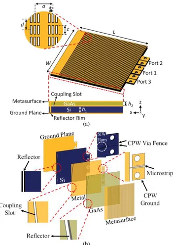
The developed metasurface antenna consists of a quasi-optical pillbox beam former loaded with a metasurface layer, as depicted in Fig. 1.
(a)
(b)
Fig. 1. Metasurface antenna: (a) pillbox structure loaded with the metasurface layer. Cross-section of the antenna in the xz-plane is shown as inset (bottom). Dimensions: a=0.85 mm, b=0.17 mm, c=tapered from 0.38 mm to 0.4 mm, d=0.53 mm, h1=0.35 mm, h2=0.175 mm, W=L=50 mm (b) individual layers of the antenna separated for visualization. The electrical size of the aperture is 56λg
x 56λg, where λg is the guided-mode wavelength in GaAs at 94 GHz.
The pillbox feeding structure generates the reference field illuminating the metasurface and, thus, the required phase gradient to steer the beam in the azimuthal plane [20]. This feature makes the analytical modeling of the guided-mode extremely simple. As shown in Fig. 1, the pillbox feeding network consists of two layers: a highly resistive (10 kΩ.cm) silicon (Si) layer (εr=11.9) with a thickness of 350 µm, and a
gallium arsenide (GaAs) layer (εr=12.8) with a thickness of 175
µm. The Si material is chosen because its standard 350 µm wafer thickness is vital to ensure that the pillbox design can be fabricated without breaking it. The GaAs material is chosen because it is possible to grow Schottky diodes on it to dynamically modulate the metasurface layer in the future. It should be noted that realizing the total thickness of the metasurface antenna with only GaAs material is not feasible, and hence the Si/GaAs architecture is adopted in this design. Embedded within the pillbox design is a parabolic metallic reflector rim connecting the top conductive plane (above GaAs) and the bottom ground plane (below Si). Between the Si and GaAs semiconductor layers, a middle conductive layer hosts a long slot bordering the parabolic reflector and coupling the Si and GaAs layers.
B. Metasurface Antenna Design
The metasurface antenna consists of three main parts: the feeding architecture, the pillbox coupler, and the metasurface.
1) Feeding architecture: as depicted in Fig. 1, the pillbox
structure is fed by three CPW ports. As shown in Fig. 2 for port 1 in detail, each CPW port excites an H-plane SIW horn within the Si layer located in the focal plane of the parabolic reflector. The aperture width of the SIW H-plane horn is optimized to provide -12 dB edge tapering along the parabolic reflector. A CPW to SIW waveguide transition is adopted to feed the integrated horn as shown in Fig. 2.
Fig. 2. CPW-SIW transition of the SIW horn. Depicted for the central port only (port 1) with the other ports (port 2 and port 3) sharing the same architecture. Dimensions: e=0.05 mm, m=2 mm, wm=0.23 mm. To improve visibility, metal
layer on Si surface is shown as transparent. Not drawn to scale.
The CPWs feeding the SIW horns are designed to be fed by 1 mm end-launch connectors. A metal pin is inserted in the horn to improve the impedance matching.
2) Pillbox coupler: the pillbox design without the
metasurface layer is shown in Fig. 3. The concept of pillbox feeding architecture was used in several antenna configurations in the literature, e.g. [20], [21]. As a difference with previous work, the stack-up is made by material with different thickness and dielectric constants. The role of the pillbox system is to transform the cylindrical wave generated by the SIW horn to a
ACCEPTED MANUSCRIPT
planar wave front with the desired phased gradient feeding the metasurface in the top GaAs layer.
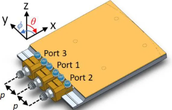
Fig. 3. Pillbox with the input ports fed through 1mm end launch connectors. The top metasurface is replaced with solid metal for depiction (p=10.5 mm).
3) Metasurface design: following the conversion of the
cylindrical wave-front to a planar one, the guided-mode within the GaAs substrate for a feed in the focus of the pillbox beam former can be expressed as follows (using the coordinate system adopted in Fig. 3)
0 j x ref
H
H e
y
. (1)In (1), Ho is the amplitude term and β is the guided-mode
propagation constant within the GaAs layer. Considering the planar phase-front of the guided-mode reference propagating inside the GaAs layer, the mathematical modeling of the holographic metasurface can be reduced to a 1D problem along
x-axis. Leveraging the unit-cells as the radiating elements, the
array factor (AF) steering in the θ-direction can be defined as follows sin , 1 ( ) ( ) i i N j x jkx m i i AF
w e e
. (2)In (2), index i defines the unit-cell element number along the metasurface layer, and k is the free-space wavenumber. It is evident that, to steer the beam from such an aperture in the θ direction, the exponent of the exponential term needs to equal zero, suggesting that the polarizability of the unit-cells should be selected as follows
,
( )
j xi jkxisinm i
w
e
e
. (3)Therefore, it can be concluded that the phase of (3) defines a phase grating. Upon substitution of the modulation term in (3) in the AF as defined in (2), the radiation from the metasurface aperture adds constructively in the θ-direction, hence, steering the beam in the θ-direction. In this work, we choose θ=15°,
ϕ=0°and leverage slot-shaped sub-wavelength sized unit-cells
to synthesize the metasurface aperture. As a result, the metasurface layer consists of an array of sub-wavelength slot-shaped unit-cells loading the top metal of the pillbox feeding structure as depicted in Fig. 1(a) earlier. It should be noted here that the selection of the steering angle in this work, θ=15°, is
done on an arbitrary basis. Analyzing the AF equation in (2) and the polarizability distribution in (3), in theory, θ steering angle can be selected in the range of –π/2 rad. < θ < –π/2 rad.
The polarizability definition in (3) is inherently linked to the magnetic dipole radiation mechanism of the slot-shaped unit cells across the metasurface depicted in Fig. 1(a). Considering the slot-shaped geometry in Fig. 1(a), the radiation from the unit-cells can be modelled as magnetic dipoles along the y-axis. At a given frequency, the dipole moment of the ith unit cell, m
i,
is connected to the polarizability definition αm,i in (3) by means
of the magnetic field at the unit-cell location, H(ri) as [16]
, ( )
i m i i
m H r . (4) The length of the unit-cells does not exceed λg/2.5, smaller
than the resonant λg/2 limit, ensuring that they are
weakly-coupled to the guided-mode (λg denotes the guided-mode
wavelength within the GaAs substrate). Due to the weak-coupling regime, the unit-cells are weak-scatters, enabling the phase information of the guided-mode reference to be preserved as indicated in (1). In comparison to a conventional array antenna, where the free-space wavelength, λ, forms the sampling basis (conventionally as λ/2), the unit-cell size is smaller than λ/8, suggesting that the guided-mode reference-wave is sampled as a quasi-continuous reference-wave. While the slot-shaped unit-cells are easy to etch, they do not alter the phase of the holographic guided-mode reference [16]-[18]. Instead, in this work, a binary modulation scheme is applied [16]. In this scheme, the difference between the phases of reference-wave (1) and objective function (2) on the metasurface plane (z=0) is minimized, 0 ( ref z H AF
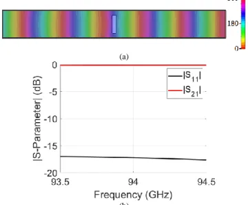
subject to maximized aperture directivity and minimized side lobe levels. The optimization goal for the design process was to simultaneously achieve a minimum directivity of 30 dBi and a maximum sidelobe level of -10 dB. As a result, this phase difference threshold was optimized to be 60° by means of full-wave simulations in CST Microwave Studio. This suggests that for points where the phase of (3) exceeds the selected threshold, no unit-cell is present. Contrarily, for points where the phase of (3) remains below the selected threshold, a unit-cell is present, coupling to the guided-mode and radiating into free-space. Increasing the phase threshold beyond the optimized limit, we observe a significant reduction in the constructive interference fidelity, reducing the overall directivity of the antenna and substantially increasing the sidelobe levels. Contrarily, reducing the phase threshold below this limit results in a substantial decrease in the number of unit-cells, limiting the efficiency of the aperture.As a further design aspect, in order to optimize the aperture efficiency and ensure that the guided-mode reference is attenuated by the time it reaches the end of the propagation path across the metasurface layer, the length of the slot-shaped unit-cells is gradually tapered along the x-axis in a linear fashion, increasing from 0.38 mm to 0.4 mm. To demonstrate the weak-scattering regime for the unit-cells forming the metasurface, in Fig. 4, we study a simple parallel-plate waveguide design using a GaAs substrate and a 0.4 mm long unit-cell etched in the top surface. It is evident that the phase profile of the guided-mode reference presented in Fig. 4(a) does not exhibit a strong perturbation caused by the presence of the unit-cell, weakly coupling to the guided-mode. The scattering parameters (S-parameters) in Fig. 4(b) also confirm this observation.
ACCEPTED MANUSCRIPT
(a)(b)
Fig. 4. Demonstration of the weak-scattering regime for the unit-cells (a) phase profile at 94 GHz of the guided-mode reference in the presence of a single unit-cell. The top conductive layer with the etched unit-cell is shown as semi-transparent to improve visibility. The slot-shaped unit-cell is seen in the center (b) S-parameter results with |S11| and |S21| are reported as -17.6 dB and -0.16 dB at 94 GHz. The size of the waveguide is 5 mm x 0.53 mm while the slot dimensions are 0.085 mm x 0.4 mm. Color bar is in degree scale.
III. RESULTS AND DISCUSSION
The metasurface antenna was fabricated in-house at NASA’s Jet Propulsion Laboratory (JPL) with the metal layers of the pillbox structure being realized by means of a variant of the semiconductor micromachining process developed by JPL [22]. The details of the fabrication process used for this antenna will be reported in another dedicated publication. A picture of the gold-coated Si-wafer during through-etch process is shown in Fig. 5(a) whereas a picture of the gold coated GaAs layer with the metasurface on top is shown in Fig. 5(b).
(a)
(b)
Fig. 5. Picture from the fabrication process: (a) silicon wafer in the middle of through-etch, (b) the etched metasurface layer onto the GaAs substrate.
A close-up picture of the fabricated CPW feeding port and the SIW H-plane horn within the Si-layer is shown in Fig. 6. An important fabrication challenge was the realization of the vertical parabolic reflector rim used to collimate the beam in the upper GaAs layer. A scanning electron microscope (SEM) image of the reflector rim is shown in Fig. 7. Further analysis on the profile of the fabricated reflector rim suggests that a surface roughness of less than 40 µm is achieved on the reflector rim, corresponding to smaller than λg/20 at 94 GHz
operating frequency. Following the fabrication campaign of the metasurface antenna, the performance metrics of the antenna were characterized using JPL’s in-house antenna measurement facilities. Because the overall thickness of the antenna is only 525 microns, a supporting metallic structure was adopted to ensure mechanical stability during the characterization process as shown in Fig. 8.
Fig. 6. Fabricated CPW feed and H-plane SIW horn in Si-layer.
Fig. 7. SEM image of the GaAs reflector wall.
Fig. 8. Fabricated Si/GaAs metasurface antenna placed on a supporting structure for characterization.
The scattering parameters (S-parameters) of the metasurface antenna are shown in Fig. 9 across 93-95 GHz frequency band.
ACCEPTED MANUSCRIPT
Fig. 9. S-parameter patterns for the Si-GaAs metasurface antenna.At the operating frequency, 94 GHz, the reflection coefficient values at port 1, port 2 and port 3 are recorded to be below -15 dB, suggesting that the metasurface antenna is impedance matched at the input ports. The coupling level between port 1 and port 3 (|S13|) is below -20 dB while the
coupling between port 2 and port 3 (|S23|) is reported as -10.5
dB at 94 GHz. Albeit remaining below -10 dB, this weak coupling between ports 2 and 3 is due to the direct reflections from the reflector rim in the direction of port 3 when port 2 is activated. However, it should be noted that the ports of the developed metasurface are to be sequentially activated, and hence, this coupling level is not a concern for this design.
The radiation pattern of the metasurafce antenna was measured using a planar near-field scanner available at JPL for W-band frequencies whereas the simulations were carried out in CST Microwave Studio. Figs. 10 and 11 demonstrate the simulated and measured radiation patterns of the metasurface antenna when fed through port 1, port 2 and port 3, respectively.
(a)
(b)
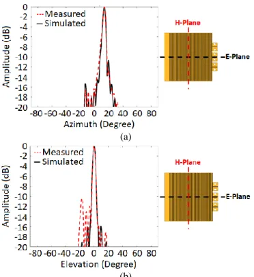
Fig. 10. Simulated and measured far-field directivity radiation patterns at 94 GHz (port 1). (a) E-plane (El = 0°). (b) H-plane (Az = 15°).
(a)
(b)
Fig. 11. Simulated and measured far-field directivity radiation patterns at 94 GHz (port 2). (a) E-plane (El = 45°). (b) H-plane (Az = 10°).
The simulated and measured radiation patterns of the metasurface antenna exhibit a good agreement. Discrepancies around the sidelobe levels can be attributed to slight deviations from the tight fabrication tolerances of the metasurface antenna and also the possible variations between the Si and GaAs dielectric permittivity values in the fabricated and simulated metasurface designs. As shown in Fig. 10, when fed through the central port (port 1), the metasurface antenna forms a beam steered at (θ=15°, ϕ=0°) with the antenna directive gain being recorded as 31.9 dBi (measured) and 31.9 dBi (simulated). Similar to the work presented in [23], we use the directivity of the metasurface to calculate the aperture efficiency, which is reported to be 59% for this scenario. Activating port 2, as shown in Fig. 11, the metasurface steers at (θ=10°, ϕ=45°), with the antenna directive gain recorded as 28.4 dBi (measured) and 28.7 dBi (simulated). We note that when excited through port 3, the radiation pattern of the metasurface antenna exhibits a mirrored behavior in comparison to port 2 due to the geometrical symmetry with the pointing angle of the main lobe being (θ=10°, ϕ=-45°). The full-wave simulation of such an electrically large metasurface antenna can be computationally expensive, and for the radiation pattern simulations in Figs. 10 and 11, we leveraged a graphics processing unit (GPU) based hardware acceleration process to parallelize the time-domain solver in CST.
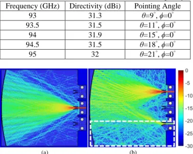
It should be noted that because port 2 (and port 3) is offset from the aperture center by 10.5 mm along the y-axis, when port 2 is activated, a smaller aperture area is used as depicted for -12 dB tapering in Fig. -12. This is because the tapering level outside the highlighted area in Fig. 12 remains below -12 dB in amplitude and hence the effective aperture size for -12 dB
ACCEPTED MANUSCRIPT
tapering excludes the highlighted region. This results in a smaller effective aperture size for -12 dB tapering level. Combined with the scanning loss, we report a drop of around 3 dB in directivity when port 2 is used. To increase the effective aperture size, one can change the position, orientation and tapering provided by the H-horn, resulting in similar performances with respect to the excitation through the central port (port 1). As evidenced earlier from S-parameter analysis shown in Fig. 9, the increased coupling between port 2 and port 3 is evident when the metasurface is excited through port 2 (or port 3 due to reciprocity) in Fig. 12(b). Although the metasurface antenna is designed to operate at 94 GHz, changing the operating frequency results in steering the beam in the elevation plane, with the frequency-dependent radiation characteristics of the antenna summarized in Table I (port 1).
Table I. Radiation characteristics as a function of frequency.
Frequency (GHz) Directivity (dBi) Pointing Angle 93 31.3 θ=9°, ϕ=0° 93.5 31.5 θ=11°, ϕ=0° 94 31.9 θ=15°, ϕ=0° 94.5 31.5 θ=18°, ϕ=0° 95 32 θ=21°, ϕ=0° (a) (b)
Fig. 12. Illumination of the reflector rim (a) port 1 (b) port 2: Aperture region outside the -12 dB taper is highlighted. Color bar is in dB scale.
IV. CONCLUSION
We have demonstrated a Si/GaAs metasurface antenna design operating at 94 GHz. It has been shown that the developed metasurface antenna provides beam shaping in a holographic manner and beam steering. The former phenomenon involves the modulation of the guided-mode reference by the metasurface layer, eliminating the need for complex phase-shifting circuits. It has been demonstrated, numerically and experimentally that the developed metasurface antenna can steer its radiation pattern by simply switching between its input ports with a maximum directivity of 31.9 dBi at the operating frequency of 94 GHz. The developed metasurface antenna offers a planar architecture, particularly suitable for air-borne platforms where aerodynamic constraints can be of great importance. A potential application for the proposed metasurface antenna is remote sensing instrumentation for NASA’s Earth Science missions. The presented design methodology can readily be scaled to other frequencies and the proposed metasurface can be adopted across a variety of other applications, from communications to wireless power transfer and millimeter-wave imaging.
REFERENCES
[1] C. L. Holloway, E. F. Kuester, J. A. Gordon, J. O'Hara, J. Booth, and D. R. Smith, “An overview of the theory and applications of metasurfaces: the two-dimensional equivalents of metamaterials,” IEEE Antennas Propag. Mag., vol. 54, no. 2, pp. 10-35, Apr. 2012.
[2] C. Pfeiffer and A. Grbic, “Metamaterial Huygens surfaces: tailoring wave fronts with reflectionless sheets,” Phys. Rev. Lett., vol. 110, pp. 197401, 2013.
[3] A. Epstein and G. V. Eleftheriades, “Huygens’ metasurfaces via the equivalence principle: Design and applications,” J. Opt. Soc. Am. B, vol. 33, no. 2, pp. 31-50, 2016.
[4] C. A. Balanis, Antenna Theory: Analysis and Design, 3rd edition, John Wiley & Sons, New York, 2016.
[5] R. C. Hansen, Phased Array Antennas, Wiley Series in Microwave and Optical Engineering, vol. 213 John Wiley & Sons, New York, 2009. [6] R. K. Kostuk, “Holography principles and applications,” 1st edition, CRC
Press, 2019.
[7] J. W. Goodman, “An introduction to the principles and applications of holography,” Proc. IEEE, vol. 59, no. 9, pp. 1292-1304, 1971.
[8] D. Smith, O. Yurduseven, B. Livingstone, and V. Schejbal, “Microwave imaging using indirect holographic techniques,” IEEE Antennas Propag. Mag., vol. 56, no. 1, pp. 104-117, Feb. 2014.
[9] R. K. Amineh, J. McCombe, and N. K. Nikolova, “Microwave holographic imaging using the antenna phaseless radiation pattern,” IEEE Antennas Wireless Propag. Lett., vol. 11, pp. 1529-1532, 2012. [10] D. Smith, M. Leach, M. Elsdon, and S. J. Foti, “Indirect holographic
techniques for determining antenna radiation characteristics and imaging aperture fields,” IEEE Antennas Propag. Mag., vol. 49, no. 1, pp. 54-67, Feb. 2007.
[11] A. Arboleya, J. Laviada, and F. Las-Heras, “Scalar calibration for broadband phaseless antenna measurements based on indirect off-axis holography,” IEEE Trans. Antennas Propag., vol. 66, no. 6, pp. 3241-3246, Jun. 2018.
[12] B. H. Fong, J. S. Colburn, J. J. Ottusch, J. L. Visher and D. F. Sievenpiper, "Scalar and Tensor Holographic Artificial Impedance Surfaces," IEEE Trans. Antennas Propag., vol. 58, no. 10, pp. 3212-3221, Oct. 2010. [13] S. Pandi, C. A. Balanis, and C. R. Birtcher, “Design of scalar impedance
holographic metasurfaces for antenna beam formation with desired polarization,” IEEE Trans. Antennas Propag., vol. 63, no. 7, pp. 3016-3024, Jul. 2015.
[14] G. Minatti, M. Faenzi, E. Martini, F. Caminita, P. De Vita, D. Gonzalez-Ovejero, M. Sabbadini, and S. Maci, “Modulated metasurface antennas for space: synthesis, analysis and realizations,” IEEE Trans. Antennas Propag., vol. 63, no. 4, pp. 1288-1300, Apr. 2015.
[15] A. M. Patel and A. Grbic, “A printed leaky-wave antenna based on a sinusoidally-modulated reactance surface,” IEEE Trans. Antennas Propag., vol. 59, no. 6, pp. 2087-2096, Jun. 2011.
[16] D. R. Smith, O. Yurduseven, L. P. Mancera, P. Bowen, and N. B. Kundtz, “Analysis of a waveguide-fed metasurface antenna,” Phys. Rev. Appl., vol. 8, no. 5, pp. 054048-1 – 054048-16, 2017.
[17] O. Yurduseven, D. L. Marks, T. Fromenteze, and D. R. Smith, “Dynamically reconfigurable holographic metasurface aperture for a Mills-Cross monochromatic microwave camera,” Opt. Express, vol. 26, pp. 5281-5291, 2018.
[18] O. Yurduseven and D. R. Smith, “Dual-polarization printed holographic multibeam metasurface antenna,” IEEE Antennas Wireless Propag. Lett., vol. 16, pp. 2738-2741, 2017.
[19] N. Chahat et al., "Advanced CubeSat Antennas for deep space and Earth science missions: a review," IEEE Antennas Propag. Mag., vol. 61, no. 5, pp. 37-46, Oct. 2019.
[20] M. Ettorre, R. Sauleau, and L. Le Coq, “Multi-beam multi-layer leaky-wave siw pillbox antenna for millimeter-leaky-wave applications,” IEEE Trans. Antennas Propag., vol. 59, no. 4, pp. 1093-1100, Apr. 2011.
[21] A. Gomez-Torrent et al., "A Low-Profile and High-Gain Frequency Beam Steering Subterahertz Antenna Enabled by Silicon Micromachining," IEEE Trans. Antennas Propag., vol. 68, no. 2, pp. 672-682, Feb. 2020 . [22] G. Chattopadhyay, T. Reck, C. Lee, and C. Jung-Kubiak,
“Micromachined packaging for Terahertz systems,” Proc. IEEE, vol. 105, no. 6, pp. 1139-1150, Jun. 2017.
[23] M. Faenzi, D. González-Ovejero, and S. Maci, “Wideband active region metasurface antennas,” IEEE Trans. Antennas Propag., vol. 68, no. 3, pp. 1261-1272, Mar. 2020.