Any correspondence concerning this service should be sent to the repository administrator:
[email protected]
O
pen
A
rchive
T
oulouse
A
rchive
O
uverte (
OATAO
)
OATAO is an open access repository that collects the work of Toulouse researchers
and makes it freely available over the web where possible.
This is an author -deposited version published in:
http://oatao.univ-toulouse.fr/
Eprints ID: 3813
To link to this article: DOI:10.1016/j.tsf.2009.03.232
URL:
http://dx.doi.org/10.1016/j.tsf.2009.03.232
To cite this version: Barnabé, Antoine and Lalanne, M. and Presmanes, Lionel and
Soon, J.M. and Tailhades, Philippe and Dumas, C. and Grisolia, J. and Arbouet, A. and
Paillard, Vincent and BenAssayag, G. and van den Boogaart, M.A.F. and Savu, V. and
Brugger, J. and Normand, P. ( 2009) Structured ZnO-based contacts deposited by
non-reactive rf magnetron sputtering on ultra-thin SiO2/Si through a stencil mask. Thin Solid
Films, vol. 518 (n° 4). 1044-1047 . ISSN 0040-6090
Structured ZnO-based contacts deposited by non-reactive rf magnetron sputtering on
ultra-thin SiO
2
/Si through a stencil mask
A. Barnabé
a,⁎
, M. Lalanne
a, L. Presmanes
a, J.M. Soon
a, Ph. Tailhades
a, C. Dumas
b, J. Grisolia
b, A. Arbouet
c,
V. Paillard
c, G. BenAssayag
c, M.A.F. van den Boogaart
d, V. Savu
d, J. Brugger
d, P. Normand
eaUniversité de Toulouse CIRIMAT UPS-INP-CNRS 118 Route de Narbonne, 31062 Toulouse, France b
Université de Toulouse LPCNO INSA-UPS-CNRS 135 avenue de Rangueil, 31077 Toulouse, France
c
CEMES-CNRS & Université de Toulouse, groupe nMat, 29 rue Jeanne Marvig 31055 Toulouse, France
d
Ecole Polytechnique Fédérale Lausanne (EPFL), Lab. de Microsystèmes, CH-1015 Lausanne, Switzerland
eInstitute of Microelectronics, NCSR‘Demokritos’, 15310 Aghia Praskevi, Greece
a b s t r a c t
Keywords: Thinfilm Nanostructure Stencil mask ZnO Si SiO2In this paper, we study the localized deposition of ZnO micro and nanostructures deposited by non-reactive rf-magnetron sputtering through a stencil mask on ultra-thin (10 nm) SiO2layers containing a single plane of
silicon nanocrystals (NCs), synthetized by ultra-low energy ion implantation followed by thermal annealing. The localized ZnO-deposited areas are reproducing the exact stencil mask patterns. A resistivity of around 5 × 10− 3Ω cm is measured on ZnO layer. The as-deposited ZnO material is 97% transparent above the wavelength at 400 nm. ZnO nanostructures can thus be used as transparent electrodes for Si NCs embedded in the gate-oxide of MOS devices.
1. Introduction
The discovery of intense emission of visible light from porous
silicon in 1990 [1] induced a large work for integration of
nanostructured silicon materials (e.g. in the form of nanocrystals: NCs) in electronics and optoelectronics (usually restricted to III–V semiconductors). Unfortunately, these efforts did not produce any tangible applications, but it is believed that undiscovered potential exists for light-emitting diodes and waveguides for optical inter-connections. Layers of transparent conducting oxides (TCOs) are very important for the modern electronic industry due to the need for transparent electrodes in applications such as thinfilm transistors (TFT) used in displays or solar cells. Among the TCOs, thinfilms of zinc oxide (ZnO) based materials have been reported to display good conductivity and high transparency in the visible region[2]. ZnO is cheap and abundant. It is also non-toxic and can be deposited at low substrate temperature. Therefore ZnO-based materials have been considered as transparent electrodes for solar cells [3], field effect transistors[4,5]and lasers [6]. For such reasons, coupling Si NCs to ZnO as a transparent electrode is very meaningful for future applications.
Furthermore, fabrication of micro/nanostructures made of metal, oxide and polysilicon[7–9]on substrates without the need for resist materials can be achieved by using stencil-assisted deposition. This
technique has shown many capabilities, for example, 15 nm resolution
[10], possibility of alignment with a 1 μm accuracy [11,12] and replication of isolated island patterns[13]. On the one hand, we have already demonstrated the combination of using a stencil mask and ion implantation for the fabrication of Si NCs in well-defined regions of SiO2 layers [14]. On the other hand, we have deposited highly
conductive (resistivity of 5 × 10− 3 Ω cm) and transparent (overall transmittance in the visible spectra of approximately 91%) doped ZnO thin film on conventional glass substrate by non-reactive radio-frequency (rf) magnetron sputtering[15].
In this work, we propose to combine these two approaches and report on the deposition of ZnO by non-reactive rf-magnetron sputtering through a stencil mask to form isolated arrays of ZnO dots above Si NCs synthesized and embedded on ultra-thin SiO2/Si
layer. The properties of the ZnO thinfilm, Si-NC–SiO2, as well as the
ZnO dot/Si-NC–SiO2 structures are examined by SEM (Scanning
Electron Microscopy), TEM (Transmission Electron Microscopy), EDS (Energy Dispersive X-ray Spectroscopy), electrical and optical measurements.
2. Results and discussion
2.1. Si NCs synthesis by ULE ion implantation
A 10 nm thick dry silicon dioxide layer wasfirst grown on an 8-inch. p-type (100)-oriented Si wafer and subsequently implanted with
Corresponding author.
silicon ions. The implantation dose and ion energy were 1 × 10¹⁶Si+/
cm2 and 1 keV, respectively. Then, the sample was annealed for
various durations ranging from 30 to 240 min, at 1050 °C under N2
ambient. During the annealing process, phase separation between the excess silicon and the oxide occurs and NCs are formed. See[16–18]
for detailed description on the sample preparation process. Energy-filtered transmission electron microscopy (EFTEM) is performed to extract the size, the density and the surface coverage of implanted regions. For example, the plane-view EELS/STEM (Electron Energy Loss Spectroscopy/Scanning Transmission Electron Microscopy) images of silicon NCs for samples annealed for 90 min at 1050 °C under N2shows a layer of spherical NCs with a density of 1.2 × 10¹²/
cm2and an average diameter of 3.2 nm (±0.5 nm) occupying 11% of
the total surface area. The corresponding figure is presented in reference[16].
2.2. ZnO deposition through stencil masks
Subsequently, ZnO:Ga micro and nanostructures were deposited onto the Si-NC/SiO2 films through a stencil mask using the same
deposition conditions as described above. The stencil masks were fabricated using a combination of deep ultraviolet (DUV) lithography and standard micro-electromechanical processing[19]. They are made
up of four 500μm×500 μm SiN membranes bored with an array of
micro and nanoapertures. The thickness of the SiN membranes ranges from 100 to 500 nm. The apertures have size and pitch ranging from 220 nm to 4μm, and 1 μm to 10 μm respectively. They can even be smaller (25 nm) if they are fabricated by electron beam lithography.
Fig. 1a shows a SEM picture of the stencil mask containing
micrometric patterns (5μm long, 1.5 μm wide with a 3 μm pitch).
Fig. 1b is a SEM picture of the smallest hole made in the stencil mask. The stencil mask was directly attached to the silica surface by double-sided adhesive tape before it was introduced into the non-reactive rf-magnetron sputtering apparatus, where ZnO:Ga thinfilms were deposited. The homemade ceramic target was composed of 2% Ga-doped zinc oxide with the wurtzite structure. The deposition
system was an Alcatel A-450 conventional planar system. The target was pre-sputtered using an argon plasma for 10 min to remove surface contamination before the deposition process. ZnO:Ga thinfilms were grown within an argon gas environment at various working pressures. The deposition power wasfixed to 50 W with a target-to-substrate distance of 5 cm. Both target and substrate were continuously water-cooled.
Fig. 1c is a SEM image exhibiting the plan view of ZnO deposited through the stencil mask. It clearly shows that the localized ZnO-deposited areas reproducing the stencil mask patterns. Moreover,
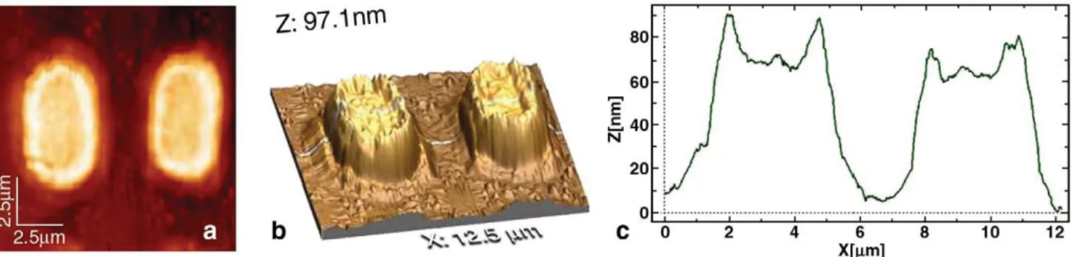
Fig. 2a shows that the deposited ZnO pattern is very close in dimension to the stencil pattern (only 3% larger). After deposition, AFM measurement reveals that the ZnO layer thickness is around 75 nm with a roughness (Ra) close to that of ZnO layer deposited on a bare wafer. These measurements are consistent with the SEM observations.
These results clearly indicate that the ZnO layer does not diffuse onto the substrate and that the gap between the stencil and the substrate is small enough to limit any blurring phenomenon. Energy dispersive spectroscopy (EDS) carried out in a scanning electron microscope (SEM) at 5 keV confirms these results. Indeed, onFig. 3a, we superimposed the spectra measured from two points as indicated in the inset: point #1 is located on top of a ZnO dot while point #2 a SiO2/Si area far away from ZnO.
Fig. 3a reveals that Zn is only found on point #1 (blue curve). More convincingly, Fig. 3b shows the spectra taken from a line scanned along two ZnO contacts as shown onFig. 3a. The zinc spectrum exhibit peaks over a distance which is fully compatible with the ZnO pitch-to-pitch distance while the silicon peak is almost constant across. These results confirm that even though the temperature of the sample may rise up to a few tens of degree Celsius during deposition due to heating by high energy incident particles, there is no significant diffusion of ZnO outside the areas defined by the apertures of the stencil mask. These results demonstrate that non-reactive rf-magnetron sputtering is an appropriate technique for the deposition of such ZnO-based materials. The ability to vary the apparatus configurations and
Fig. 1. SEM images of the stencil mask: (a) micrometric patterns and (b) nanometric patterns (c) ZnO structures deposited through the stencil lithography.
parameters allows versatility and fine control over the defect chemistry of the depositedfilms. Indeed, operating under a plasma with relatively low oxygen partial pressure leads to good electrical conductivity due to non-stoichiometric ZnO. This is directly obtained in the as-depositedfilms; no post-annealing is required, thus avoiding the diffusion of Zn into the Si substrate or the silicon dioxide layer. Using optimized deposition conditions which are less severe, i.e. minimization of the various electronic, ionic and atomic bombard-ments, substrate heating during deposition and interfacial diffusion can be reduced.
2.3. Electrical and optical properties
The conduction measurements are performed in ambient air at room temperature using a linear four-point setup. As-deposited Ga-doped ZnO layers exhibit an electrical resistivity of about 6.45 × 10− 3Ω cm when deposited on the SiO2/Si layer. These values are a
slightly lower than that obtained by e-beam deposition technique with an electron energy of ~ 6 keV in vacuum[21]. Two similar MOS structures which were fabricated using aluminium and ZnO as gate respectively exhibit similar I–V characteristics[22]. The conductiv-ity of the ZnO thinfilms deposited on fused silica substrate can be
optimized by changing the pressure deposition [23] but with a
modification to the deposition temperature and thin layer micro-structure. As the conductivity of ZnO is not limiting the properties of the fabricated MOS devices, the rf-sputtering deposition con-ditions are kept unchanged. In fact, the resistance of ZnO is low compared to the total resistance of the fabricated device (ZnO/ SiO2/Si), whereby the resistance ranges from MΩ to TΩ (not shown
here).
A subsequent 20 min annealing at 400 °C under N2+ H2decreases
the resistivity to 5 × 10− 3Ω cm in accordance to the fact that the conduction is primarily dominated by electrons generated from the oxygen vacancies V0 and zinc interstitial atoms Zni[24], which are
enhanced by annealing. As the ZnO layer resistance is not critical, we decided to use the as-deposited Ga doped ZnO to avoid any additional diffusion which may contaminate the underlaying silicon NCs.
Next, a 75 nm ZnO layer was deposited on a fused silica substrate to perform absorbance and transmittance measurements.Fig. 4shows the transmittance spectra of the as-deposited and annealed samples. It is obvious that the as-deposited and annealed ZnO layers exhibit roughly the same transmittance spectra: around 95% and 97% at 400 nm wavelength respectively. Wavelengths above 400 nm are not absorbed by the ZnO layer which makes it suitable for light excitation from Si NCs embedded in a SiO2layer using a laser emitting at the
wavelength of 488 nm. The photo-luminescence of several samples will be tested to see if the presence of ZnO will result in reduction of the emission characteristics Si nanocrystals.
3. Conclusions
In conclusion, Ga doped ZnO nanostructures have been deposited using non-reactive rf-magnetron sputtering on ultra-thin SiO2/Si
through a stencil mask. Ultra low energy ion implantation was
performed onto an ultra-thin SiO2 layer (10 nm), followed by
annealing to produce 2D arrays of Si NCs. Next, the Ga-doped ZnO nanostructures were deposited on top of this substrate. AFM and SEM show that the ZnO-based nanostructures have sharp features and roughness comparable to the bare ZnO layer deposited under the same conditions. The electrical resistivity of the ZnO layer is around 6.45 × 10− 3Ω cm (as-deposited) and 5×10− 3Ω cm (annealed) far
below the total resistance of the fabricated MOS structure. The extracted transmittance spectra show that as-deposited and annealed samples exhibit roughly the same transmittance of around 95% and 97% respectively at a wavelength of 400 nm. Hence, this process makes ZnO of good transparency and good electrical characteristics even for the as-deposited samples. This makes ZnO a good candidate as transparent nanostructured electrodes for MOS devices containing few Si NCs embedded in the SiO2layer. The next study will involve the
fabrication of transparent ZnO conducting electrodes that will
self-aligned with the Si NCs pockets made by “stencil mask ion
implantation process”. References
[1] L.T. Canham, Appl. Phys. Lett. 57 (1990) 1046. [2] T. Minami, MRS Bull. (2000) August 2000.
[3] K. Westermark, H. Rensmo, A.C. Lees, J.G. Vos, H. Siegbahn, Phys. Chem. B 106 (2002) 10108.
[4] Z. Fan, D. Wang, P.C. Chang, W.Y. Tseng, J.G. Lu, Appl. Phys. Lett. 85 (2004) 5923. [5] Z. Fan, J.G. Lu, Appl. Phys. Lett. 86 (2005) 032111.
[6] M.H. Huang, S. Mao, H. Feick, H. Yan, Y. Wu, H. Kind, E. Weber, R. Russo, P. Yang, Science 292 (2001) 1897.
[7] G. Kaminsky, J. Vac. Sci. Technol., B 3 (1985) 741.
Fig. 4. Transmittance spectra of as-deposited and annealed ZnO layers. Annealing conditions used are 400 °C for 20 min under N2+ H2ambient.
Fig. 3. EDS spectra of elements detected in the sample: Zn, O, Si. (a) Superimposition of spectra obtained from points no. 1 and no. 2 as marked in the inset (b). (c) Zn and Si spectra of the line crossing two ZnO dots as marked in the inset (b).
[8] M. Graff, S.K. Mohanty, A.B. Frazier, J. Microelectromech. Syst. 13 (2004) 956. [9] M.M. Deshmukh, D.C. Ralph, M. Thomas, J. Silcox, Appl. Phys. Lett. 75 (1999) 1631. [10] G. Kim, B. Kim, J. Brugger, Sens. Actuators, A 107 (2003) 132.
[11] J. Arcamone, M. van den Boogaart, F. Serra-Graells, S. Hansen, J. Brugger, F. Torres, G. Abadal, N. Barniol, G. Pérez-Murano, IEEE International Electron Devices Meeting, San Francisco, USA, 2006.
[12] A. Tixier, Y. Mita, J.P. Gouy, H. Fujita, J. Micromechanics Microengineering 10 (2000) 157.
[13] W.H. Bruenger, M. Torkle, K.N. Leung, Y. Lee, M.D. Williams, H. Loeschner, G. Stengl, W. Fallmann, F. Paschke, G. Stangl, I.W. Rangelow, P. Hudek, Microelectron. Eng. 46 (1999) 477.
[14] C. Dumas, J. Grisolia, L. Ressier, A. Arbouet, V. Paillard, G. Ben Assayag, A. Claverie, M.A.F. van den Boogaart, J. Brugger, Phys. Status Solidi, A 204 (2007) 487. [15] A. Barnabé, M.S.D. Darma, E. Mugnier, I. Pasquet, L. Presmanes, C. Bonningue and
Ph. Tailhades, IWNA 2007 (1st Int. Workshop on Nanotechnol. and Appl.), Vung Tau, Vietnam, 9– 12 November 2007, 85–87 (2007).
[16] C. Bonafos, M. Carrada, N. Cherkashin, H. Coffin, D. Chassaing, G. Ben Assayag, A. Claverie, T. Müller, K.H. Heinig, M. Perego, M. Fanciulli, P. Dimitrakis, P. Normand, J. Appl. Phys. 95 (2004) 5696.
[17] J. Grisolia, C. Dumas, G. BenAssayag, C. Bonafos, S. Schamm, A. Arbouet, V. Paillard, M.A.F. van den Boogaart, J. Brugger, P. Normand, Superlattice and Microstructures, 2008,doi:10.1016/j.spmi.2007.12.013.
[18] J. Grisolia, M. Shalchian, G. BenAssayag, H. Coffin, C. Bonafos, S. Schamm, S.M. Atarodi, A. Claverie, Nanotechnology 16 (2005) 2987.
[19] M.A.F. van den Boogaart, G.M. Kim, R. Pellens, J.-P. Vand Den Heuvel, J. Brugger, J. Vac. Sci. Technol., B 22 (2004) 6.
[20] I. Horcas, R. Fernandez, J.M. Gomez-Rodriguez, J. Colchero, J. Gomez-Herrero, A.M. Baro, Rev. Sci. Instrum. 78 (2007) 013705.
[21] N.R. Aghamalyan, I.A. Gambaryan, E.Kh. Goulanian, R.K. Hovsepyan, R.B. Kostanyan, S.I. Petrosyan, E.S. Vardanyan, A.F. Zerrouk, Semicond. Sci. Technol. 18 (2003) 525.
[22] C. Dumas, J. Grisolia, J. Carrey, A. Arbouet, V. Paillard, G. BenAssayag and S. Schamm, M.A.F. van den Boogaart, V. Savu and J. Brugger, P. Normand and M. Shalchian. Submitted to Microelectronics Engineering (2008).
[23] M. Lalanne, A. Barnabé, M.S.D. Darma, I. Pasquet, L. Presmanes and Ph. Tailhades, Submitted to Thin Solid Films Special Issue IS-TCO 2008 (2008).
[24] F.A. Kröger, The Chemistry of Imperfect Crystals, North-Holland, Amsterdam, 1964, p. 650.