HAL Id: tel-01743849
https://pastel.archives-ouvertes.fr/tel-01743849
Submitted on 26 Mar 2018HAL is a multi-disciplinary open access archive for the deposit and dissemination of sci-entific research documents, whether they are pub-lished or not. The documents may come from teaching and research institutions in France or abroad, or from public or private research centers.
L’archive ouverte pluridisciplinaire HAL, est destinée au dépôt et à la diffusion de documents scientifiques de niveau recherche, publiés ou non, émanant des établissements d’enseignement et de recherche français ou étrangers, des laboratoires publics ou privés.
Reliability analysis of spintronic device based logic and
memory circuits
You Wang
To cite this version:
You Wang. Reliability analysis of spintronic device based logic and memory circuits. Electronics. Télécom ParisTech, 2017. English. �NNT : 2017ENST0005�. �tel-01743849�
EDITE - ED 130
Doctorat ParisTech
T H `
E S E
pour obtenir le grade de docteur d ´elivr ´e par
T ´el ´ecom ParisTech
Sp ´ecialit ´e - ´
Electronique et Communications
pr´esent´ee et soutenue publiquement par
You WANG
le 13 F´evrier 2017
Analyse de Fiabilit ´e de Circuits Logiques et de M ´emoire bas ´es sur Dispositif
Spintronique
Directeur de th `ese: Lirida Alves de Barros NAVINER Co-directeur de th `ese: Weisheng ZHAO
Composition du Jury
Damien Deleruyelle, Professeur, Institut National des Sciences Appliqu ´ees de Lyon Pr ´esident
Ian O’CONNOR, Professeur, ´Ecole Centrale de Lyon Rapporteurs
Lionel TORRES, Professeur, Universit ´e Montpellier 2
Christian Gamrat, Directeur de Recherche au CEA Examinateur
Lirida Alves de Barros NAVINER, Professeur, T ´el ´ecom ParisTech Directeurs de Th `ese Weisheng ZHAO, Professeur, Universit ´e de Beihang
TELECOM ParisTech
´ecole de l’Institut Mines-T´el´ecom - membre de ParisTech
Circuits
c
Le D´epartement Communications et Electronique (COMELEC) LTCI, CNRS, T´el´ecom ParisTech, Universit´e Paris-Saclay 46 Rue Barrault, Paris CEDEX 13, 75634, France
This thesis is set in Computer Modern 11pt, with the LATEX Documentation System
c
You Wang 2017
Je souhaite commencer ce manuscrit par adresser mes remerciements sinc`eres aux person-nes qui m’ont beaucoup aid´e depuis trois ans et qui ont contribu´e `a l’ach`evement de ce m´emoire. Cette th`ese a ´et´e men´ee dans le cadre des travaux du groupe NANOARCHI (Cir-cuits et Architectures pour Nanodispositifs ´emergents) du d´epartement Nano´eelectronique au laboratoire Institut Fondamentale Electronique (IEF) et du groupe SEN (Syst`emes Electroniques Num´eriques) du d´epartement COMELEC (communication et ´electronique) `
a T´el´ecom ParisTech.
Je voudrais tout d’abord adresser mes remerciements `a mes directeurs de th`ese, Madame Lirida Naviner, Professeur `a T´el´ecom ParisTech et Monsieur Weisheng Zhao, Professeur `a l’Universi´e de Beihang, qui m’ont accueilli dans leur ´equipe et qui m’ont soutenu tout au long des trois ans de travail. Leur confiance en mes capacit´es et leur grande patience lors de nos ´echanges r´eguli`eres m’ont beaucoup encourag´e et motiv´e. Je tiens `a les remercier ´egalement de m’avoir aid´e `a exploiter des d´emarches de recherche scientifique et `a r´esoudre des probl`emes scientifiques ou administratifs.
Je voudrais ensuite remercier les membres de mon jury de leur temps consacr´e `a ma th`ese. Je remercie particuli`erement, mes rapporteurs Professeurs Ian O’CONNOR et Lionel TORRES pour le regard critique et leurs remarques constructives sur mon travail. Je remercie ´egalement Professeur Damien Deleruyelle et M. Christian Gamrat, qui ont gentiment accept´e d’examiner mes travaux de th`ese.
J’aimerais aussi adresser mes remerciements `a M. Hao Cai, pour les discussions efficaces et les suggestions originales de sa part durant la r´ealisation des id´ees innovantes tout au long de cette th`ese, entre autre, sur les avantages de la techonologie FDSOI 28nm, M. Yue Zhang, pour ses aides me permettant approfondir la compr´ehension du sujet de th`ese, de la mod´elisation du MTJ et des premiers pas de la r´edaction scientifique, et Mlle. Erya Deng, pour le d´emarrage de cette th`ese et la simulation des circuits de base `a l’aide du logiciel Cadence.
Aussi, un grand merci aux services administratifs de l’IEF et de T´el´ecom ParisTech, dont Mme. Chantal Cadiat, Mme. Yvonne Bansimba, Mme. Elisabeth Valensi, Mme. Sylviane
ii
Thomas, Mme. Florence Besnard, Mme. Marianna Baziz... Grace `a leur travail scrupuleux et efficace, j’ai pu profiter de ma vie `a l’´ecole sans me soucier des probl`emes administratifs et concentrer sur mon sujet de recherche. Je tiens `a remercier tous mes coll`egues de T´el´ecom ParisTech et de l’IEF, de leur gentillesse et de leur accompagnement. Leurs conseils voire les causeries men´es pendant les d´ejeuners ou les pauses ont beaucoup enrichi mes connaissances profesionnelles ainsi que ma vie quotidienne. C’est avec grand plaisir de travailler entre eux.
Naturellement, je voudrais aussi remercier tous mes amis fran¸cais et chinois: la famille de Fr´ed´erique Bedouin, qui m’a montr´e la vie familiale fran¸caise et les coins int´eressants de Paris, Zhaohao Wang, Yu Zhang, Gefei Wang, Yao Wu, Mengying Ren, Pengwenlong Gu, Yimeng Zhao, ...pour leur accompagnement durant les trois ans.
Enfin, je souhaite exprimer profonde gratitude `a ma famille, dont notamment, mes parents, M. Jianlin Wang et Mme. Yurui Yang, qui m’ont accompagn´e et soutenu san condition pour l’aboutissement de ce travail.
Abstract
Moore’s law has successfully guided us in the research and development of integrated circuits (IC) for several decades. However, power dissipation issue has recently become the bottleneck for further scaling down of complementary metal oxide semiconductor (CMOS) technology node. This issue can not be overcome by the conventional semiconductor de-vices. Nanotechnologies and nano-devices are considered approaches to build up ultra low power IC in the next era of “More than Moore”. For instance, spintronics devices such as magnetic tunnel junction (MTJ) feature non-volatility and 3D integration, which can turn off the standby power and reduce drastically the power dissipated in data traffic be-tween memory and logic chips. Moreover, the spintronics devices are promising to operate normally in sub 0.1V, which is another bottleneck of semiconductor devices. Compared with its counterparts, MTJ nanopillar with interfacial perpendicular magnetic anisotropy (PMA-MTJ) becomes an outstanding candidate for spin transfer torque magnetic random access memory (STT-MRAM) because of its lower switching current, faster operation speed, high scalability and better thermal stability.
However, spintronics devices suffer from significant reliability issues, e.g., process vari-ation, stochastic switching behavior, temperature fluctuation and dielectric breakdown. As a result, the performance of hybrid MTJ/CMOS circuits can be significantly degraded by these issues. The reliability becomes one of the most critical factors to limit the use in practical applications. Thus, it is essential to study, analyze and reduce/tolerate the impact of these issues on the yield of MTJ based circuits at the early design phase for economic reasons. For this purpose, a compact model including all of the reliability issues is required by the circuits designers. We proposed a model of PMA-MTJ switched by STT mechanism which comprises the main reliability issues. In order to achieve good agreement with the experimental measurements, several physical models which describe the issues and realistic parameters are integrated in the compact modeling. The model is programmed in VerilogA language for SPICE compatible simulation.
Based on the accurate model of PMA-STT-MTJ, the robustness of typical hybrid MTJ/CMOS circuits is entirely investigated, e.g., MRAM writing/reading circuit, mag-netic flip-flop (MFF), magmag-netic full-adder (MFA). With detailed analysis of the simulation results, we proposed some design methodologies to improve the circuits robustness, such
iv
as using high performance devices (e.g., fully depleted silicon on insulator (FDDOI)) and applying dynamic asymmetrical body bias in symmetrical circuits of FDSOI transistors.
Instead of weakening the impact of reliability issues, some of them can be beneficial to several special applications. For instance, the stochastic switching behavior can be used as a physical randomness source in the security area. We proposed a novel circuit design of true random number generator (TRNG) and compared the performance with conventional realization. Furthermore, the uncertainty in MTJ switching process also provides a new approach of low power inexact circuit design, e.g., approximate computing and stochastic computing.
Keywords: Magnetic tunnel junction, Reliability analysis, Compact model, Dy-namic asymmetrical body bias, True random number generator, Approximate computing, Stochastic computing
Remerciements i
Abstract iii
List of Tables ix
List of Figures x
List of Acronyms xxi
1 Introduction 1
1.1 Motivations . . . 1
1.2 Thesis contributions . . . 4
1.3 Organization of the thesis . . . 5
2 State of the art 7 2.1 Magnetic tunnel junction . . . 7
2.1.1 MTJ working principles . . . 7
2.1.2 MTJ switching approaches . . . 10
2.1.2.1 Field-induced magnetic switching (FIMS) . . . 11
2.1.2.2 Thermally assisted switching (TAS) . . . 12
2.1.2.3 Spin transfer torque (STT) . . . 13
2.1.2.4 Thermally assisted spin transfer torque (TAS+STT) . . . . 15
2.1.2.5 Spin Hall effect spin transfer torque (SHE+STT). . . 15
2.2 Magnetic tunnel junction based memories and logic circuits . . . 17
2.2.1 Magnetic Random Access Memory . . . 17
vi CONTENTS
2.2.3 Other novel applications . . . 22
2.3 Reliability analysis of MTJ device and MTJ based applications . . . 23
2.4 Summary . . . 27
3 Compact modeling of reliability issues in STT-PMA-MTJ 29 3.1 Perpendicular magnetic anisotropy (PMA) MTJ . . . 29
3.2 Reliability issues of STT-PMA-MTJ . . . 31
3.2.1 Process variation . . . 31
3.2.2 Stochastic switching behavior of MTJ . . . 34
3.2.3 Temperature fluctuation behavior of MTJ . . . 34
3.2.4 Dielectric breakdown . . . 35
3.3 Physical models of PMA-MTJ. . . 36
3.3.1 Tunnel barrier resistance model . . . 37
3.3.2 Bias-voltage-dependent TMR model . . . 38
3.3.3 Model of static behavior . . . 39
3.3.4 STT switching dynamic model . . . 39
3.4 Physical models of reliability issues in MTJ . . . 40
3.4.1 Process variation . . . 40
3.4.2 Stochastic switching . . . 41
3.4.3 Temperature fluctuation behavior of MTJ . . . 41
3.4.3.1 Models of temperature sensitive parameters . . . 42
3.4.3.2 Temperature fluctuation due to Joule heating. . . 44
3.4.4 Dielectric breakdown . . . 46
3.4.4.1 Breakdown voltage. . . 46
3.4.4.2 Prediction of lifetime . . . 48
3.4.4.3 Breakdown probability . . . 49
3.4.4.4 TDDB phenomena submitted to voltage pulse stress . . . . 49
3.5 Compact modeling in EDA tool Cadence. . . 51
3.5.1 Modeling language: Verilog-A . . . 51
3.5.2 Electrical Modeling of MTJ under Cadence . . . 53
3.5.2.1 Hierarchy of the physical models integrated in the compact model . . . 53
3.5.2.2 Parameters of the compact model and Component Descrip-tion Format (CDF) . . . 53
3.5.2.3 Schematic view of model and relative circuit in the design
environment . . . 55
3.5.3 Functionality validation of model . . . 59
3.6 Fast simulation model using worst-case corners . . . 64
3.6.1 Introduction of worst-case fixed corners model . . . 64
3.6.2 Worst-case fixed corners model of MTJ . . . 65
3.7 Conclusion . . . 67
4 Reliability analysis and variability-aware design of hybrid MTJ/CMOS circuits 69 4.1 Reliability analysis of MTJ based circuits . . . 69
4.1.1 Variability analysis of MTJ based circuits . . . 70
4.1.2 Influence of MTJ stochastic switching behavior on MTJ/CMOS cir-cuits . . . 70
4.1.3 Temperature impact on MTJ based circuits . . . 72
4.1.4 Ageing of MTJ based circuits . . . 73
4.1.5 Application of non Monte-Carlo Methodology in hybrid MOS/MTJ Circuits . . . 77
4.1.5.1 Switching delay and time to failure estimation of 1T-1M memory array . . . 77
4.1.5.2 Variability-aware energy-delay analysis of PCSA based STT-MRAM cell . . . 78
4.1.5.3 Worst-case analysis of magnetic full-adder dynamic perfor-mance . . . 79
4.1.5.4 Results discussion . . . 80
4.2 Reliability-aware design of MTJ-based circuits . . . 81
4.2.1 Transistors with UTBB-FDSOI technology . . . 82
4.2.2 Circuit Design of non-volatile Flip-Flop using dynamic asymmetrical body bias of FDSOI . . . 83
4.2.3 Reliability analysis and performance evaluation . . . 84
4.3 Conclusion . . . 89
5 Novel applications of MTJ in conventional circuits 91 5.1 A novel circuit design of MTJ based true random number generator . . . . 91
viii CONTENTS
5.1.2 Circuit design of true random number generator using MTJ . . . 92
5.1.3 Simulation results . . . 95
5.1.4 Performance evaluation and optimization . . . 96
5.2 Realization of Stochastic computing using MTJ . . . 98
5.2.1 Introduction of stochastic computing . . . 98
5.2.2 Stochastic computation with combinational logic . . . 99
5.2.3 Stochastic computing using STT-MTJ . . . 99
5.2.4 Case Study: Polynomial function RTL synthesis . . . 102
5.3 Approximate computing method using MTJ . . . 103
5.3.1 Introduction of approximate computing . . . 103
5.3.2 Design for Approximation . . . 104
5.3.2.1 Reduced Logic Complexity . . . 104
5.3.2.2 The Dual-mode MFA . . . 105
5.3.2.3 Functional Simulation . . . 106
5.3.3 Design Considerations . . . 107
5.3.3.1 Supply Scaling Strategy . . . 107
5.3.3.2 Performance Analysis . . . 109
5.3.3.3 Reliability-aware Simulation . . . 110
5.4 Conclusion . . . 113
6 Conclusions and Perspectives 115 6.1 Conclusions . . . 115
6.2 Perspectives . . . 117
Bibliography 119
A Source code of STT-PMA-MTJ compact model 141
B List of publications 153
2.1 Comparison of performance for the different switching approaches [28] . . . 17 2.2 Performance comparison of the universal memory candidates widely used
and appeared in the last decade: F represents feature size of the lithogra-phy, the energy estimation is on the cell-level (not on the array-level), the endurance is signified by the writing cycles [39, 42].. . . 19 2.3 Comparison of different compact models of MTJ . . . 27
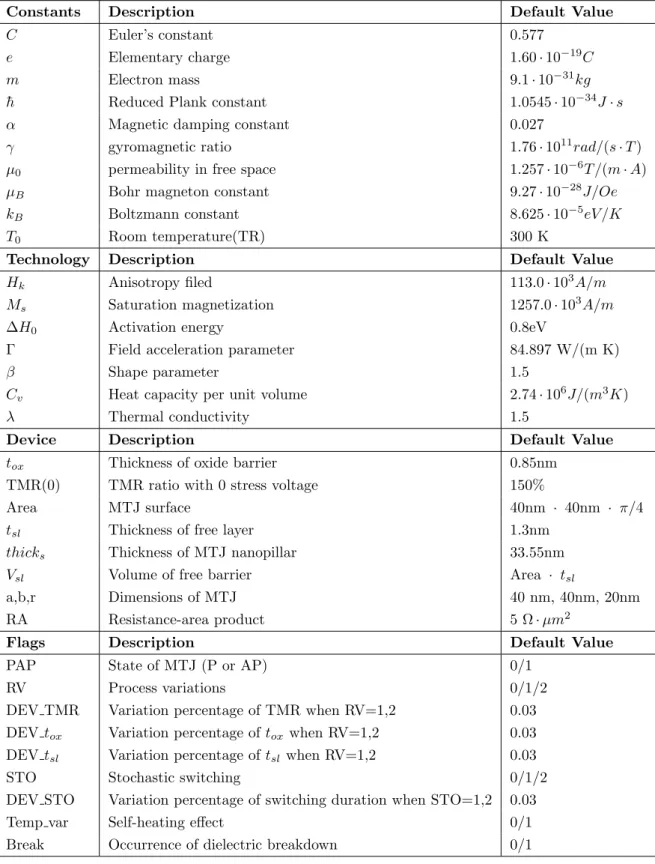
3.1 Parameters integrated in the compact model including constants, technol-ogy parameters, device parameters and reliability control flags. . . 58 3.2 Parameters settings of CMOS transistors. . . 65
4.1 Design parameters settings . . . 70 4.2 Worst-case corners setting of transistor and MTJ models for worst-case
performance analysis of STT-MRAM cell . . . 79 4.3 Model precision on function of n and transistors size . . . 82 4.4 Comparison of performance between proposed methodology (DABB) and
conventional method (NBB) . . . 89
5.1 Comparison of performance in TRNG . . . 98 5.2 Performance comparison of conventional MFA and proposed approximate
adder. . . 112
B.1 Comparaison de performance de MFA conventionnel et MFA approximatif props´es. . . 185
1.1 Breakthroughs in spintronics research and development for memory. . . 3
2.1 Equivalent resistance model to describe GMR effect in the structure of non-magnetic (NM) layer sandwiched by two ferromagnetic (FM) layers: Anti-parallel (AP) state presents higher resistance value than parallel (P) state.. . . 8
2.2 Spin-dependent tunneling of electrons in an MTJ while the magnetization directions in two FM layers are (a) parallel and (b) anti-parallel. . . 9
2.3 MTJ consists of three layers: two ferromagnetic layers separated by an oxide barrier. The nanopillar resistance (Rp, Rap) depends on the corresponding state of the magnetization of the two ferromagnetic layers Parallel (P) or Anti-Parallel (AP). The MTJ state can be switched by modulating the magnetic field. . . 10
2.4 Field induced magnetic switching approach structure. . . 11
2.5 Thermally assisted switching approach structure. . . 12
2.6 Spin transfer torque switching approach structure. . . 13
2.7 Diagram of the LLG equation: Γdamping is the Gilbert damping torque, ΓST T is the STT term and Γf ield is the effective field torque generated by effective magnetic field Hef f. . . 14
2.8 Thermally assisted spin transfer torque switching approach structure. . . . 15
2.9 Spin Hall effect spin transfer torque switching approach. . . 16
2.10 A schematic of the cross-point array. The selector is added in series with the MRAM cell at each cross-point.. . . 18
xii LIST OF FIGURES
2.12 General architecture of logic in memory based on STT-MRAM: Mx repre-sents the highest level of metal in CMOS technology. . . 20 2.13 Typical MOS/MTJ NV-LIM circuits based on pre-charge sense amplifier
structure: logic gates, full adder and flip-flop. . . 21 2.14 Implementation of ASL Boolean gates. Only the net spin polarization is
shown for spin current. (a) Inverter. (b) NAND. “F” denotes a magnet with fixed magnetization direction. . . 23 2.15 Low state resistance and high state resistance distributions of the 4kbit
circuit with MTJ size of 120 x 170 nm as demonstrated in [41]. Bias voltage is kept at -0.1 V. . . 24 2.16 Experimental measurement of STT stochastic switching behaviors, the
switch-ing duration follows a certain distribution determined by the current and pulse duration. . . 25 2.17 TMR ratio at different temperature in experimental measurements in [7, 8,
11, 12].. . . 26
3.1 (a) Structure of PMA STT MTJ based on CoFeB/MgO stack. (b) Core of MTJ and switching mechanism. . . 30 3.2 Typical flow of magnetic tunnel junction (MTJ) device fabrication, which
mainly consists of stack deposition, patterning, etching dielectric encapsu-lation, and connecting. . . 32 3.3 Magnetic curves (measured by NanoMOKE) of MTJ stacks annealed at
different annealing times. The film stack deposited by magnetic sputtering processing are exsitu annealed at 300◦C for different annealing times (40, 60 and 90 min) with perpendicular H = 0.775 T in a high vacuum chamber. 33 3.4 The precession of magnetization under the influence of a spin current: Time
dependence of (a) Mz and (b) Mx, (c) The reversal process of magnetic moment. θ and φ represent the initial state of free layer magnetic moment. For PMA-MTJ, the switching behavior is mainly dependent on initial value of θ. . . 35 3.5 Three main breakdown mechanisms for MTJ barriers: Pinhole and shunt
are soft-breakdown mechanisms that are typically lower than the intrinsic dielectric breakdown voltage [71]. . . 37 3.6 The TMR ratio of MTJ is dependent on the bias voltage. . . 38
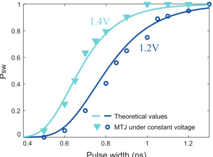
3.7 Switching probability Psw as a function of pulse width: the lines are the-oretical values plotted from (3.18) and the markers are statistical results from 1000 times of Monte Carlo simulation under Cadence. . . 42 3.8 Temperature dependence of effective anisotropy field Hk and saturation
magnetization Ms. . . 44 3.9 Temperature dependence of thermal stability factor and of MTJ based chip
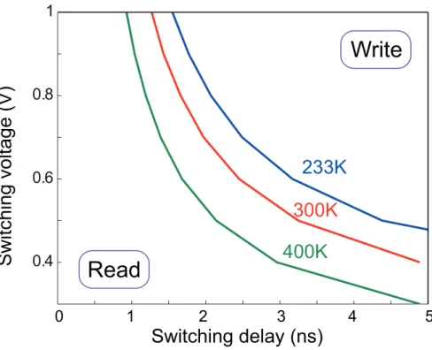
failure rate with 8 bits per word, different reading duration and different reading current. . . 45 3.10 Switching voltage versus average switching time at different temperature
conditions.. . . 45 3.11 Temperature evaluation of MTJ during current pulses. . . 46 3.12 Breakdown voltage for different configuration (P or AP) and stress voltage
(positive or negative) versus MgO thickness, the markers are experimental results from [72] (tox=1.8nm, 2.1nm) and [21] (tox=0.9nm). . . 47 3.13 The MTJ state is changed as the applied voltage is higher than the critical
switching voltage (VcP, VcAP). The resistance is steeply degraded beyond breakdown voltage (VbP, VbAP). . . 48 3.14 Time-to-failure statistics of MTJ at different stress voltages (tox=1.25nm).
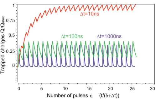
The time value corresponding to 0 of Weibull function represents 63% failure time. . . 50 3.15 Number of voltage pulses before breakdown (η) versus interval between
voltage pulses (∆t) with δ=30ns and τ =100ns. . . 50 3.16 Number of voltage pulses before breakdown (η) versus interval between
voltage pulses (∆t) with δ=30ns and τ =100ns. . . 52 3.17 Architecture of PMA STT MTJ compact model integrating physical models
of reliability issues. . . 54 3.18 Component Description Format (CDF) in Cadence.. . . 56 3.19 (a)Symbol of the PMA-STT-MTJ compact model (b) Symbol at circuit level. 57 3.20 Schematic of pre-charge sense amplifier circuit. . . 57 3.21 MC simulations of (a)bias voltage dependent resistance and (b) 1000
com-plete writing process with process variations. . . 59 3.22 MC simulations of 1000 complete writing process with the stochastic
be-haviors. The switching duration is set following a normal distribution with variation of 0.02. . . 60
xiv LIST OF FIGURES
3.23 Switching probability as a function of applied switching voltage and switch-ing time.. . . 61 3.24 TMR evolution with temperature increase and the experimental data (red
points) in [99]. . . 61 3.25 Resistance of MTJ versus bias voltage with different temperatures. Critical
current is reduced by increasing temperature. . . 62 3.26 Dependence of reading error rate on the thickness of oxide barrier tox and
area of MTJ. . . 63 3.27 Lifetime of MTJ without (dashed lines) and with (lines) consideration of
self-heating. The dots are experimental data in [74]. . . 63 3.28 Simulation results of statistical model (1000 MC simulations) and
worst-cases model (TT, FF, and SS): (a) current and (b) switching delay of MTJ in different states (P or AP) with a voltage pulse(σ=0.01 and n=3). . . 67
4.1 Architecture of pre-charge sense amplifier based STT-MRAM cell circuit proposed in [49]. It consists of two parts: writing control part and PCSA part. . . 71 4.2 Transient simulations of 4T-2M writing circuit and PCSA circuit.. . . 71 4.3 Dependence of reading error rate on the thickness of oxide barrier tox and
area of MTJ. . . 72 4.4 Switching probability with different writing voltages: the dashed lines are
theoretical values plotted from equation (3.18) and the markers are statis-tical results of MC simulation. . . 73 4.5 (a) Switching probability as a function of applied switching voltage and
switching time. (b) Switching voltage versus average switching time at different temperature conditions. . . 74 4.6 Reading error rate of PCSA with different area of circuit (SA is the
mini-mum size of PCSA circuit) under different temperature conditions. . . 74 4.7 Cumulative breakdown probability distribution for theoretical case (dashed
lines), the simulation results of MTJ under constant voltage (circles) and MTJ integrated in CMOS circuit (stars).. . . 75 4.8 The studied symmetrical MFF is composed of two parallel MTJs, the
writ-ing block, a clocked sense amplifier, NAND-based slave SR latch and feed-back loop. . . 76
4.9 HBD failure gate current density: the breakdown sensitivity of transistor in MFF circuit. . . 76 4.10 Switching delay and time to failure of memory arrays: the cross are from
1000 elements of memory arrays with statistical model; the blue dot line is the Weibull function of the cross in which F signifies the failure probability of the memory elements; the triangles are from 1 element with the worst-case model (σ=0.01 and n=3). . . 78 4.11 Writing and sensing performance of STT-MRAM cell: the stars and dots are
from statistical model (1000 MC simulations); the frames are from worst-case model of MTJs (σ=0.01 and n=4.5) and CMOS transistors. . . 80 4.12 Performance of delay time and dynamic energy in MFA circuit: the stars
and dots are from statistical model (1000 MC simulations); the frames are from worst-case model of MTJs and CMOS (σ=0.01 and n=3). Two different discharge transistor sizes are considered: W/L=200nm/30nm and W/L=500nm/30nm. . . 81 4.13 The thin film devices in FDSOI technology with a cross-section view of
pla-nar/2D structure FDSOI CMOS. Body bias voltage can impact transistor performance. Poly bias is achieved by additional gate length. . . 83 4.14 Variability FDSOI: A single NMOS transistor works in saturation region.
The coefficient of Vthvariation is analyzed among FBB, nominal design (no body bias) and FBB. . . 84 4.15 (a) Pre-charge sense amplifier with dynamic asymmetrical bias bias (b) RC
circuits generate the body bias voltages for transistors in PCSA. . . 85 4.16 Waveform of proposed Non-volatile flip-flop circuit using dynamic
asym-metrical body bias. . . 86 4.17 Reading error rate of the proposed NVFF versus different TMR value: FBB
means dynamic asymmetrical body bias, and NBB means nominal body bias. 86 4.18 Reading error rate of the NVFF versus process variations: MTJ parameters
tsl , tox, T M R follow normal distribution around the mean value µ with the deviation σ. . . 87 4.19 Reading error rate of the proposed NVFF versus different supply voltage:
FBB means asymmetrical forward body bias, and NBB means nominal body bias. . . 88
xvi LIST OF FIGURES
4.20 Reading error rate of the proposed NVFF versus different thermal con-ditions: FBB means asymmetrical forward body bias, and NBB means nominal body bias. . . 88
5.1 Switching probability of MTJs on function of switching current with 10ns pulse. The current with 50% switching success is indicated above. This figure is obtained by 1000 runs of Monte-Carlo simulation with the same MTJ under voltage pulses.. . . 93 5.2 Architecture of proposed MTJ-based true random number generator: The
random writing circuit generates a switching current to write the MTJs with 50% success and it is controlled by the correction block; The MTJ writing part enables MTJ switching (generating random number or resetting to initial state); The correction block composed of counter and comparator is used to execute real-time output probability tracking and send feedback to writing block. . . 94 5.3 MTJ writing circuit and PCSA: Iswis the switching current flowing through
MTJ during random writing phase and Ir is the switching current during reset phase. Nc0, Nc1and Nc2modulate the switching current according to the random number probability obtained in the precedent cycle. . . 95 5.4 The phase transition diagram of proposed circuit design: The three states in
blue frame are with different output random number probability after reset phase; The state in green signifies the unknown switching probability after random writing phase; The three states in yellow are with different known random number probability after sensing phase. For MTJs, ‘0’ represents P state and the resistance is relatively low. ’ ?’ represents unknown information. 96 5.5 Time-domain diagram of proposed true random number generator. During
each cycle, the MTJs are firstly reset to the initial state (with Ir=178µA for P state and Ir=142µA for AP state), then randomly switched, and finally sensed at the output. The initial current is set for 50% of switching success. 97 5.6 Output ‘1’ probability versus number of clock cycles: The output random
number probability becomes stable after 30 cycles (The probability of ‘1’ occurrence stays around 50%) for all the five corner models. . . 97 5.7 Examples: SC based on two input combinational logic (AND, OR, XOR
5.8 Proposed stochastic bit generator with 4T1M structure. 1000 runs monte-carlo simulation illustrates the stochastic behavior of MTJ. . . 100 5.9 Simulation result: switching probability versus MTJ operation current.. . . 101 5.10 Layout of 4T1M SNM with 28nm FDSOI process. . . 101 5.11 Polynomial function synthesis with traditional binary signal. . . 102 5.12 An example of polynomial function synthesis. . . 103 5.13 Conventional CMOS approximate adders: AXA1, AXA2 and AXA3 [183]. . 105 5.14 Circuit implementation of two approximate MFAs: AX-MFA1 (without
dashed line box) and AX-MFA2. The first approximate AX-MFA1 is im-plemented with conventional simplified logic: input Ci in dashed rectangle is eliminated to get an approximate Sum = A ⊗ B. The second dual-mode approximate AX-MFA2 is implemented with the whole schematic. . . 106 5.15 The transition simulation waveforms of approximate adder with reduced
logic complexity (AX-MFA1). Output Sum is with errors. . . 107 5.16 The transient simulation waveforms of approximate adder by insufficient
writing current (AX-MFA2).. . . 108 5.17 Supply voltage strategy in bi-mode MFA. . . 108 5.18 Cross-sectional view of dynamic well FDSOI MOS devices. Different well
configurations impact circuits performance. . . 109 5.19 4.41µm*1.98 µm Layout with planar 28nm FDSOI technology. A 16nm
poly bias is used to reduce leakage power and enhance yield. LVT-RVT strategy is performed in layout, single P-well covers nMOS RVT transistor (in sense amplifier) and pMOS LVT transistor (in logic network). . . 110 5.20 Latency simulation of dual-mode MFA. A 152.7 ps latency is realized in
approximate Sum operation when Vdd=0.5V. Continuous supply scaling down to sub-Vtregion leads to large latency (1.27 ns when Vdd=0.36V). . . 110 5.21 Probability with respect to Vdd scaling. MOS/MTJ process variations and
MTJ stochastic effect influence MFA probability. . . 111 5.22 Sensing probability with respect to Vdd considering process variation.
Dif-ferent well configurations impact sensing error rate. Single N-well doping method achieves the extra Vdd margin. . . 112
xviii LIST OF FIGURES
B.2 Effet tunnel d´ependant du spin des ´electrons dans un MTJ, tandis que les directions d’aimantation dans les deux couches FM sont (a) parall`eles et (b) en antiparall`ele.. . . 160
B.3 Structure standard de MTJ. . . 161
B.4 Sch´ematique de (a) cross-point array et (b) 1T/1MTJ m´emoire cellule ar-chitecture . . . 163
B.5 Circuits typiques de MOS/MTJ NV-LIM bas´es sur une structure d’amplificateur de d´etection de pr´e-charge : portes logiques, additionneur complet et bascule.164
B.6 Architecture du mod`ele compact de PMA STT MTJ int´egrant des mod`eles physiques de probl`emes de fiabilit´e. . . 168
B.7 Les simulations MC de (a) la r´esistance d´ependante de la tension de po-larisation et (b) 1000 processus d’´ecriture complet avec des variations de processus. . . 169
B.8 (a) Simulations de MC de 1000 processus d’´ecriture compl`ete avec les com-portements stochastiques. (b) Probabilit´e de commutation en fonction de la tension de commutation et du temps de commutation. . . 170
B.9 (a) Evolution du TMR avec augmentation de la temp´erature et donn´ees exp´erimentales (points rouges) dans [99]. (b) R´esistance du dispositif MTJ par rapport `a la tension de polarisation `a diff´erentes temp´eratures. Le courant critique est r´eduit en augmentant la temp´erature. . . 170
B.10 Dur´ee de vie de MTJ sans (lignes pointill´ees) et avec (lignes) prise en con-sid´eration de l’auto-´echauffement. Les points sont des donn´ees exp´erimentales dans [74]. . . 171
B.11 (a) Taux d’erreur de lecture versus l’´epaisseur de MgO et la surface de MTJ. (b) Probabilit´e de commutation avec diff´erentes tensions d’´ecriture. . . 172
B.12 (a) Probabilit´e de commutation en fonction de la tension de commutation et du temps de commutation appliqu´es. (b) Tension de commutation en fonction du temps moyen de commutation `a des temp´eratures diff´erentes. . 173
B.13 (a) Taux d’erreur de lecture du PCSA avec la surface diff´erente du circuit (SA est la taille minimum du circuit de PCSA) dans diff´erentes conditions thermiques. b) Distribution cumulative de probabilit´e de claquage. . . 173
B.14 Performance d’´ecriture et de lecture de la cellule STT-MRAM: les ´etoiles et les points sont issus du mod`ele statistique (1000 simulations MC); Les trames viennent du mod`ele le plus d´efavorable de MTJs ( sigma = 0.01 et n = 4.5) et de transistors CMOS. . . 175 B.15 Variabilit´e FDSOI: Un seul transistor NMOS fonctionne dans la r´egion de
saturation. Le coefficient de Vth variation est analys´e entre FBB et la con-ception nominale (sans biais corporel) et FBB. . . 176 B.16 (a) Amplificateur de d´etection de pr´e-charge avec polarisation du substrat
asym´etrique dynamique (b) Les circuits RC g´en`erent les tensions de polar-isation du substrat pour les transistors dans PCSA.. . . 177 B.17 Taux d’erreur de lecture du NVFF en fonction de diff´erentes (a) tensions
d’alimentation et (b) conditions thermiques. . . 178 B.18 Architecture du circuit de TRNG propos´ee. . . 179 B.19 Diagramme temporel du circuit propos´e. . . 180 B.20 R´esultat de simulation: probabilit´e de commutation par rapport au courant
de fonctionnement MTJ. . . 181 B.21 Un example de synth`ese de fonction polynomiale. . . 182 B.22 Les simulations de transition de l’additionneur approximatif avec une
com-plexit´e logique r´eduite (AX-MFA1). La sortie Sum est avec des erreurs. . . 183 B.23 Les simulations de transition de l’additionneur approximatif avec double
mode (AX-MFA2). La sortie Sum et Co est avec des erreurs. . . 183 B.24 Simulation de latence de MFA `a double mode. . . 184
AFM Anti-Ferromagnetic
AP Anti-Parallel
ASL All Spin Logic
ASIC Application-Specific Integrated Circuit
BER Bit Error Rate
BL Bit Line
BSIM Berkeley Short-channel IGFET Model
CAD Computer-aided Design
CAM Content Addressable Memory
CDF Component Description Format
CIMS Current-induced magnetization switching
CIP Current In Plane
CMOS Complementary Metal-Oxide-Semiconductor
CPP Current Perpendicular to Plane
CPU Central Processing Unit
DC Direct Current
DRAM Dynamic Random Access Memory
xxii List of Acronyms
ECC Error Correction Circuit
EDP Energy-Delay Product
FIMS Field Induced Magnetic Switching
FM Ferromagnetic
FPGA Field Programmable Gate Array
GMR Giant MagnetoResistance
HBD Hard Breakdown
HDD Hard Disk Drive
HKMG High-K Metal-gate
IC Integrated Circuit
IEEE Institute of Electrical and Electronics Engineers
ITRS International Technology Roadmap for Semiconductors
LLG Landau-Lifshitz-Gilbert
LUT Look Up Table
MC Monte-Carlo
MFA Magnetic Full Adder
MOSFET Metal Oxide Semiconductor Field Effect Transistor
MRAM Magnetoreisistance Random Access Memory
MTJ Magnetic Tunnel Junction
MTTF Mean-Time-to-Failure
NM Non-Magnetic
NML Nanomagnetic Logic
NMOS N-Channel Metal Oxide Semiconductor
OxRAM Oxide Random Access Memory
P Parallel
PCRAM Phase-Change Random Access Memory
PCSA Pre-Charge Sense Amplifier
PDF Probability Density Function
PMA Perpendicular Magnetic Anisotropy
PVT Process-Voltage-Temperature
RA Resistance-Area Product
RAM Random Access Memory
RDF Random Dopant Fluctuations
RM Racetrack Memory
RRAM Resistive Random Access Memory
RV Resistance variation
SBD Soft Breakdown
SC Stochastic Computing
SHE Spin Hall Effect
SL Source Line
SoCs Systems-on-Chip
SOT Spin Orbit Torque
SPICE Simulation Program with Integrated Circuit Emphasis
SRAM Static Random Access Memory
STT Spin Transfer Torque
TAS Thermally Assisted Switching
xxiv List of Acronyms
TCAD Technology Computer-aided Design
TDDB Time-Dependent Dielectric Breakdown
TMR Tunnel MagnetoResistance
TRNG True Random Number Generator
TTF Time-to-Failure
Chapter
1
Introduction
1.1
Motivations
Charge and spin are the two intrinsic attributes of an electron, which determine its macro-scopic behaviors. Before the discovery of giant magnetoresistance (GMR), the investiga-tions on the charges and spins of electrons were usually considered to be independent of each other and little attention was paid to the correlation between these two attributes [1]. The charge-based devices have changed the way we create, produce and even think since their birth in 1947. With the quick development dominated by Moore’s law, the number of transistors in a dense integrated circuit (IC) have successfully doubled approximately every two years (Or 18 months from aspect of chip performance) for decades. Among all the transistor devices, complementary metal-oxide-semiconductor (CMOS) technology is the most widely used in the ICs nowadays. The development of IC in the digital age is determined by the scaling down of CMOS technology node. Moore’s prediction has been used in the semiconductor industry to guide long-term planning and to set targets for research and development for several decades.
However, the scarcity of resources such as power consumption and interconnect band-width has become the bottleneck to continue Moore’s scaling [2]. It was predicted by the International Technology Roadmap for Semiconductors (ITRS) that the memory static power in 2026 will be triple that in 2016 [3]. This trend is due to the increasing contri-bution of the leakage current to the total power consumption as CMOS technology node shrinks blow 90 nm [4]. Thus, the off-state leakage is considered as the critical obstacle for further scaling down of CMOS technology node. Meanwhile, with the emergence of cloud and internet of things (IoT), seamless interaction of big-data and instant data have become necessary. For the essential elements of IoT (e.g., sensors), emerging devices with
features of ultra low power and high performance are required to generate the data in-stantly with few consumption. From the other part, abundant computing and memory resources are required in the Big data to generate the service and the information that clients need. The conventional CMOS circuits can not meet these urgent requirements. In this background, the emerging spintronic devices which combine the two attributes of electron (charge and spin) are considered as a promising solution because of non-volatility and fast speed operation. Compared with the conventional CMOS based memories, spin-tronics based memories can retain the stored information without power supply. Moreover, with easy 3D integration, spintronic devices are deposited on the top of arithmetic units, which avoids the large data traffic of the conventional Von-Neumann architecture and thus reduces the operation latency and improves energy efficiency.
The development of spintronics devices originates from the discovery of Giant Mag-netoresistance (GMR) effect in 1988 by Albert Fert and Peter Gr¨unberg [5, 6]. From then on, many academic and industial researchers have concentrated on the emerging materials to explore better energy efficiency of spintronics devices. As one of the most important spintronics devices, magnetic tunnel junction (MTJ) is a promising candidate for the next generation of non-volatile memories. MTJ consists of one nonmagnetic layer sandwiched by two ferromagnetic layers in which the Tunnel MagnetoResistance (TMR) effect was discovered for the first time by [7] in 1975. The resistance of MTJ depends on the relative magnetization orientation of the two ferromagnetic layers (Rp at parallel
state and Rap at antiparallel state). As the MTJ resistance can be configured
compa-rable with CMOS transistors, it can be integrated in the memories and logic circuits to represent logic ‘0’ or ‘1’. Its characteristic is quantified by TMR ratio ((Rap− Rp)/Rp).
The research and development of MTJ has become intensive since the first experimental demonstration of TMR effect based on the amorphous AlxOy barrier at room temper-ature (TMR ratio was 18% and 11.8%) in 1995 [8, 9]. Even though the TMR ratio has been improved up to 70% at room temperature (RT) [10] with materials and tech-nology optimization, this low value limited the application of MTJ into CMOS circuits. The single-crystalline MgO was introduced into MTJ by Shinji Yuasa in 2004, which in-creased the TMR ratio up to 180% at RT [11]. A TMR ratio as high as 604% at 300 K in Ta/Co20Fe60B20/MgO/Co20Fe60B20/Ta pseudo-spin-valve magnetic tunnel junction was observed by Shoji Ikeda in 2008 [12], which is obtained by optimizing annealing tem-perature and suppressing the Ta diffusion into CoFeB electrodes and in particular to the CoFeB/MgO interface.
1.1 Motivations 3
As a promising memory candidate, the switching approaches of MTJ are always with intensive research. Field Induced Magnetic Switching (FIMS) was firstly employed in the early realizations of MTJ based magnetoresistive random access memory (MRAM) [13,14]. Too high currents (∼10mA) are required by this switching method to generate magnetic fields, which becomes a critical constraint for FIMS to realize high density and low power memory due to high power consumption, large die area and high disturbance. Ther-mally Assisted Switching (TAS) was proposed and by Bernard Dieny and Jean-Pierre Nozi`eres in 2003, which largely decreases the threshold of switching current [15]. In this method, a current flows into MTJ to heat the MTJ and facilitates the switching by an-other. TAS has effectively decreased the power consumption of writing operation (switch-ing current∼1mA), but the scalability issue still remains unsolved and the switch(switch-ing speed is lower due to the necessary cooling down after the heating. To address the power and scalability issue, a novel switching approach of Spin Transfer Torque (STT) was firstly predicted theoretically by John Slonczewski and Luc Berger in 1996 [16,17] and observed experimentally by many research groups in 2000 [18, 19]. This method uses a relatively low current (∼100uA) flowing through the MTJ to switch its state. Without the need of magnetic field, STT makes it possible to achieve high density and low power MRAM. MTJ with interfacial perpendicular magnetic anisotropy (PMA-MTJ) was discovered by Shoji Ikeda in 2010 [20] which features low switching current (49uA), and high thermal stability. Figure 1.1 demonstrates the evolution of the most significant breakthroughs of spintronics research and development.
Year TMR GMR MgO MTJ STT Phenomena discovery Experimental realiza!on 1975 1988 1996 2001 2004 MgO MTJ TMR at RT 1995 STT switching at RT PMA MTJ 2010 Applica!ons 2000 128 kbit 180nm MRAM 2003 TAS MTJ 65nm STT-MRAM 2005 64Mb STT-MRAM 2012 11nm MRAM 2016 TMR: Tunnel magnetoresistance GMR: Giant magnetoresistance
STT: Spin transfer torque TAS: Thermally assisted switching MRAM: Magne!c random access memory
Figure 1.1: Breakthroughs in spintronics research and development for memory.
remains very challenging due to poor reliability. As STT switching method has been demonstrated intrinsically stochastic [21], a relatively high current density is required for successfully switching in writing process. With ultra-thin layers(∼1nm) and small die area in MTJ, MTJ suffers from extreme work conditions such as intense electric field across oxide barrier and high current density flowing through it. As a result, the performance is severely degraded in terms of self-heating effect, process variations and aging mechanisms. The reliability risks can be involved from initial design to tape-out, till the final wear-out. All will have significant impact on quality and yield of MTJ based circuits.
Research work on reliability mainly concentrates on defects modeling, reliability analy-sis, reliability-aware methodology, and failure prediction [22]. Defects modeling character-izes physical defects and maps the degradation to parameters at device level (e.g., BSIM4 model), which is the basic work of the latter three. With the fast evolution of STT-MRAM, the reliability has attracted the attention of researchers( [21,23,24]). The reliability issues of MTJ have always been well characterized theoretically and experimentally. However, there exists not yet a compact model comprising all the possible reliability issues for circuit designers. With the expensive cost of MTJ fabrication, it is very profitable to identify and address the possible reliability issues and thus provide reliability-aware circuits at the early design phase.
This thesis is dedicated to provide a thorough understanding of the sources of the possible reliability issues in MTJ and propose an accurate compact model for circuit designers. This model can be used to predict the possible functional failures of MTJ based circuits and to address all the issues at the early design phase. By using this model, we have carried out reliability analysis and explored some design strategies to tolerate the reliability issues and improve the circuit performance. Finally, some novel realizations of conventional specific circuits are presented to benefit from the reliability issue of MTJ.
The thesis is part of the project “ANCD2” funded by IDEX Paris-Saclay, ANR-11-IDEX-0003-02 supported by French National research Agency (ANR). The project con-centrates on the control and diagnosis of components and devices in the application of nanotechnologies.
1.2
Thesis contributions
This thesis is focused on the reliability analysis of hybrid MTJ/CMOS circuits from device level to circuit level. The main research contributions are as follows:
1.3 Organization of the thesis 5
• Investigation of reliability issues in magnetic tunnel junction (MTJ): synthesis of the physical mechanisms and quantification by theoretical deductions.
• Compact modeling of main reliability issues in MTJ, which includes process varia-tions, stochastic switching, temperature fluctuation and dielectric breakdown.
• Proposition of a worst-case corners model for fast performance evaluation of variability-awareness. This model provides faster simulation speed while guaranteeing a high level of analysis quality, especially in very large scale circuit.
• Integration of proposed model into memory and logic circuits for reliability assess-ment to validate its functionality. The methods for performance estimation are presented in details for hybrid MTJ/CMOS circuits.
• A novel circuit design methodology for variability tolerant circuits and systems (Dy-namic asymmetrical body bias for symmetrical structure based circuits). This design features faster operation speed and less sensing errors.
• Realization of true random number generator using stochastic switching behavior of MTJ. The functionality is well confirmed and its robustness is optimized by correc-tion systems.
• New circuits of MTJ-based approximate computing and stochastic computing. The performance of these circuits are significantly improved in terms of area and power consumption.
1.3
Organization of the thesis
The organization of this thesis is as follows:
Chapter 2 presents the background of this thesis in details. We firstly introduce the physical mechanisms of spintronic devices and then concentrate on the working principles of magnetic tunnel junction (MTJ). An overview of MTJ based MRAM and computing circuits is also presented. Meanwhile, the research on reliability analysis of MTJ based circuits is studied and existing compact models of MTJ are investigated.
Chapter 3 proposes a compact model of STT-PMA-MTJ programmed in VerilogA language which includes the main reliability issues. The origins of the main reliability
issues in MTJ are well studied. The physical models used for describing the functional behaviors and reliability issues are well confirmed. After introducing the employed model-ing method and programmmodel-ing language VerilogA, the simulation results of the model are demonstrated.
Chapter 4 applies the proposed model in the hybrid MTJ/CMOS circuits to study their reliability. Based on these analysis, we explore some methodologies to improve the circuit robustness and yield probability. These methodologies are implemented in certain designs to demonstrate its feasibility and performance in terms of speed, energy consumption and area.
Chapter 5 tries to explore the usage of MTJ reliability issues in special applications. As a significant functional failure issue, stochastic switching behavior of MTJ can be appropriately inserted in the security applications as an intrinsic randomness source. We carry out the detailed circuit design and execute simulations to verify the functionality and performance. MTJ is also used in approximate computing and stochastic computing to realize low power and low complexity circuit.
Chapter 6 concludes the work realized during this thesis and presents some perspectives relative to the thesis and future research directions.
Chapter
2
State of the art
This chapter presents the preliminary work relative to the reliability of MTJ device. Firstly, the physics of MTJ are introduced in details. Then, the main applications based on MTJ are discussed and compared in terms of performance and reliability. Finally, the current status of research on main reliability issues of MTJ is reviewed and the required work is synthesized.
2.1
Magnetic tunnel junction
2.1.1 MTJ working principles
Spintronics is an emerging technology which concentrates on the correlation between the two attributes of an electron: spin and charge [1]. Before the appearance of the disci-pline Spintronics, the research is dominated by manipulating the charge of electron from classical conductors as copper to semiconductor as silicon. In these devices, there is no spin polarization because the spin direction is naturally random. The most outstanding breakthrough of Spintronics was the discovery of Giant Magnetoresistance (GMR) effect in 1988 by Fert and Gr¨unberg [5,6].
GMR effect was observed in stacks composed of thin ferromagnetic (FM) and non-magnetic (NM) layers such as metal. Naturally, electrons have two spin states: spin-up and down which are discovered in paired electrons. In FM layer, the number of spin-up (majority) and spin-down (minority) are totally different, resulting in the different contribution to electrical transport regarding to the amount of conducting electrons. This contribution is defined as spin polarization P:
P = n ↑ −n ↓
where n↑ and n↓ are the numbers of spin-up and spin-down electrons, respectively. GMR effect can be explained by a simplest form demonstrated in the Figure2.1. When injecting a current into a FM layer such as Fe and Co, only the electrons with specific spin direction will be able to pass through. Thus, if the two FM layers have parallel (P) magnetization direction, the electrons with one specific spin direction will travel through the sandwich nearly without scattering while those with opposite direction can not pass. The struc-ture behaves relatively low resistance Rp. Respectively, in the case of anti-parallel (AP)
magnetization direction, both spin-up and spin-down electrons will pass partially, leading to a relatively higher resistance Rap [13]. With special composition of materials in some
multilayers structure, the relative magnetoresistance ∆R/R = (RAP− RP)/RP can reach
100% or more. In fact, the first discovery was aready 80% in the Fe/Cr multilayer [5]. Many applications have been realized by profiting GMR effect, such as “spin valve” which has been widely used in the hard disk drives (HDDs) as read heads [25]. With intense research interest, the areal density of spin valve based HDDs has been increased by three orders of magnitude (from ∼0.1 to ∼100 Gbit/in2) between 1991 and 2003 [13].
R
pR
apFM
NM
FM
FM
NM
FM
Figure 2.1: Equivalent resistance model to describe GMR effect in the structure of non-magnetic (NM) layer sandwiched by two ferronon-magnetic (FM) layers: Anti-parallel (AP) state presents higher resistance value than parallel (P) state.
Another important breakthrough of Spintronics is the discovery of tunnel magnetore-sistance (TMR) effect by Julliere in 1975 [7], in which the non-magnetic metal layer is replaced by an insulating layer. The phenomenon can be microscopically explained from the viewpoint of band structure, which is demonstrated in Figure 2.2 [13]. In FM ma-terials, the populations of spin-up and spin-down are different at the Fermi energy level, leading to unequal density of states available for each [26]. As a result, the FM material is
2.1 Magnetic tunnel junction 9
magnetized by the net magnetic moment generated by the disequilibrium. The electrons near the Fermi level act as carriers during the transport. The spin-polarized electrons pass through the oxide barrier by tunnel effect with conservation of spin state: An electron with spin-up state from one FM layer can travel across the insulator only if it can find a spin-up state at the Fermi level of the other FM layer. If the magnetization directions of the two FM layers are parallel (P), all the spin-up and spin-down electrons can easily find a corre-sponding state after traveling through the barrier because the band structures of two FM layers are almost the same. Inversely, if they are anti-parallel (AP), only partial electrons can act as carriers for the tunneling current, resulting in a lower conductance than AP state. Thus, the resistance of the trilayer stack is different according to the magnetization state of FM layers. EF1 EF2 EF1 EF2 Parallel An!-Parallel E E E E Barrier Barrier FM FM FM FM (a) (b)
Figure 2.2: Spin-dependent tunneling of electrons in an MTJ while the magnetization directions in two FM layers are (a) parallel and (b) anti-parallel.
Magnetic tunnel junction (MTJ) is created by using this phenomenon, which induces much research effort and becomes a promising memory candidate. Figure 2.3 demon-strates a typical structure of MTJ stack which mainly consists of three layers: a thin insulator (oxide barrier such as AlxOy and MgO) sandwiched by two ferromagnetic layers (e.g., CoFe). The two FM layers are with different configurations: one with a fixed spin magnetization direction which is noted as pinned layer or reference layer; whereas the other one can be changed in two directions (storage layer, switching layer or free layer). Thus, parallel (P) and anti-parallel (AP) are usually used to describe the two different configurations of MTJ. The MTJ configuration can be tuned by switching the spin magne-tization orientation in the storage layer, which can be achieved by a magnetic field above the threshold value with opposite direction.
With oxide barrier between two ferromagnetic layers, MTJ behaves resistance value which is comparable with CMOS transistor technology. This makes it possible to detect
Pinned layer Insulator Storage layer Electrode Electrode Magne!c field Resistance AP state P state
Figure 2.3: MTJ consists of three layers: two ferromagnetic layers separated by an oxide barrier. The nanopillar resistance (Rp, Rap) depends on the corresponding state of the
magnetization of the two ferromagnetic layers Parallel (P) or Anti-Parallel (AP). The MTJ state can be switched by modulating the magnetic field.
the state of MTJ using CMOS based sense amplifier and generate logic ‘0’ and ‘1’ with specific design. TMR ratio is one of the most important parameters which determines the performance of MTJ device. It is defined as follows:
T M R = ∆R RP
= RAP − RP RP
(2.2)
where RP and RAP are the MTJ resistances of P and AP state. From the Figure 2.2,
it can be deduced that the TMR ratio is determined by the spin polarization of the FM layers, which can be expressed by2.3:
T M R = 2P1P2 1 − P1P2
(2.3)
where P1 and P2 are the spin-polarization in two FM layers which can be calculated by
equation (2.1).
For better immunity to process variations and mismatch generated in fabrication pro-cess, high TMR value is always preferred, which has been the motivation of intense research and fast development of MTJ. Recently, new ferromagnetic materials, oxide barrier and MTJ process have been exploited to achieve higher TMR value (e.g., CoFeB as FM layer and MgO as oxide barrier).
2.1.2 MTJ switching approaches
As aforementioned, the switching of MTJ state can be realized by changing the spin magnetization orientation in the storage layer. Several switching approaches have been proposed since the appearance of MTJ. This section will review these switching methods
2.1 Magnetic tunnel junction 11
and evaluate their efficiency.
2.1.2.1 Field-induced magnetic switching (FIMS)
Field Induced Magnetic Switching (FIMS) is the main switching approach in the first generation of MTJ device [27]. As depicted in Figure 2.4, the magnetic state of MTJ is written by means of a magnetic field generated by currents flowing through two orthogonal write lines. To write information in the MTJ, Ib works as the bit line which generates
a magnetic field to switch the spin magnetization direction of the storage layer while Iw operates as the word line to assist the above operation. Thus, the written state is
determined by the polarity of Ib. The two writing lines used in FIMS allow this writing
approach easy to be addressed in memory array. It can be observed in Figure2.4that the lines for sensing operation are entirely independent with those for writing. Thereby, the two operations can be asynchronous, resulting in better flexibility of hybrid circuit design of FIMS-MTJ and CMOS than other writing methods.
I
bI
wI
rI
rHb
Hw
Figure 2.4: Field induced magnetic switching approach structure.
However, the combination of two perpendicular pulses of magnetic fields should be precisely configured to execute correctly the writing selectivity. This may lead to narrow operating window induced by half-selectivity disturbance [28]. Moreover, the external fields generated also have impact on the devices nearby, which limits the realization of high density FIMS-MRAM. The most severe issue of this approach is the high currents (∼10 mA) needed to generate magnetic fields, hindering its integration with conventional CMOS transistors due to the limit of electromigration issue. In 2005, Freescale proposed and patterned the toggle switching approach , which increases the energy barrier during programming and then reduces significantly the disturbance problem. In this method,
Synthetic Anti-Ferromagnetic (SAF) layers have been used to replace one storage layer. Based on this optimization, Freescale commercialized the first MRAM product in 2006 (4 Mbit). Despite the continuous optimization, this approach can not meet the increasing demand for high speed, high density and low power in large scale MRAM designs.
2.1.2.2 Thermally assisted switching (TAS)
Thermally assisted switching (TAS) was proposed by SPINTEC laboratory to improve the performances of write selectivity, power consumption and thermal stability of MTJ [15, 29]. As illustrated in Figure2.5, an additional anti-ferromagnetic (AFM1) layer with low blocking temperature (TB2 ∼160◦C) is normally added above the storage layer and the reference layer is pinned by another (AFM2) with a much higher blocking temperature TB1 (typically∼300◦C). This configuration enhances the flexibility of storage layer and facilitates the switching while prevents any magnetization switching of the reference layer. For the write operation, a current is injected into MTJ (Ih) to heat up the FM layers
above their magnetic ordering temperature, particularly the storage layer. When the temperature exceeds TB2, the spin magnetization direction of storage layer can be easily reversed by a small magnetic field generated by (Ib). Ih is mono-directional whereas Ib is
bidirectional.
Compared with FIMS, TAS features relatively lower power, higher density and lower switching disturbance between memory cells. However, the switching speed is limited by the existence of heating and cooling duration, which make it not appropriate for high speed logic applications, such as magnetic flip-flop (MFF) and magnetic arithmetic units. In addition, the heating process increases the average temperature of the entire MTJ stack, which accelerates the breakdown of oxide barrier and results in relatively short time to failure.
I
hI
bI
hH
b An -ferromagne c layer An -ferromagne c layer lower TB2 lower TB12.1 Magnetic tunnel junction 13
2.1.2.3 Spin transfer torque (STT)
Spin transfer torque (STT) was predicted independently by Berger and Slonczewski in 1996 [16, 17], which promises much better energy efficiency and scalability than the two switching approaches presented above. From the view of electrical property, STT switching method only requires a bidirectional current I higher than the threshold current to change the state of MTJ (see Figure2.6). It was observed that a spin-polarized current injected perpendicularly to the plane could influence the magnetization of FM layers. The transfer of spin angular momentum from a spin-polarized current to a local magnetization of the FM layer can generate a large torque (noted as spin transfer torque) to the magnetization to this FM layer. This torque efficiently facilitates the magnetic manipulations of FM layers in MTJ than the aforementioned switching methods using magnetic fields alone. If the current density exceeds the threshold value, the torque applied by the current will change the magnetization of the free layer (FL) of MTJ [30].
P
I
P->API
AP->PI
P->AP> I
c0I
AP->P> I
c0AP
Figure 2.6: Spin transfer torque switching approach structure.
In STT-MTJ, the electrons injected into one FM layer are polarized and then transfer angular momentum by applying a torque on the magnetization of the other FM layer after tunneling across the oxide barrier. The basic considerations for spin-transfer torque devices can be illustrated in a single domain model, which assumes that the layers are uniformly magnetized [18, 19]. The dynamics of magnetization switching of free layer (FL) can be described by a Landau-Lifshitz-Gilbert (LLG) equation including the STT [31,32] as following equation:
∂ ~m
∂t = −γµ0m ×~ H~ef f + α ~m × ∂ ~m
where ~m represents the unit magnetic moment of the FL magnetization under the macrospin approximation, where Hef f is the effective magnetic field, which is the sum of different
magnetic fields, such as the external magnetic field, the demagnetization field and the anisotropy field, the magnetostatic field, the Oersted field and the exchange coupling field. γ is the gyromagnetic ratio, µ0 is the vacuum permeability. α is the Gilbert damping
con-stant, ¯h is the reduced Planck constant, β is the is the STT coefficient depending on both the spin polarization and the geometric configuration of the spin torque efficiency, J is the switching current density, ~mr is the unit vector of the reference layer (RL) magnetization.
This equation can be understood using Figure 2.7 [33]. On the right side of the equation, the first term represents the precession of the field-induced magnetization, the second describes the intrinsic Gilbert damping torque which reduces the precessional angle as a function of time and leads to the relaxation of the precession, the last is the STT term with the opposite direction of the damping vector which induces the switching of magnetization momentum. In such a current-induced magnetization switching MTJ, the switching is determined by the competition between damping term and the STT term. For instance, the STT term generated by a small current is relatively weaker than the damping term, leading to unchanged magnetization direction. Contrarily, the STT term generated by a high current is stronger than the damping term, resulting in larger precessional angles and eventual state switching. The two regimes are distinguished by the threshold current (noted as critical current Ic0).
H
effm
Γ
STTΓ
dampingΓ
fieldPrecession
Figure 2.7: Diagram of the LLG equation: Γdamping is the Gilbert damping torque, ΓST T
is the STT term and Γf ield is the effective field torque generated by effective magnetic
field Hef f.
2.1 Magnetic tunnel junction 15
the switching process. Furthermore, the magnitude of current required by STT is sig-nificantly reduced comparing with the previous switching methods (normally less by an order). Consequently, higher density and faster speed can be achieved in STT-MTJ based MRAM. Since its practical demonstration, STT switching approach is considered as the most promising candidate for the future MRAM applications.
2.1.2.4 Thermally assisted spin transfer torque (TAS+STT)
Thermally assisted spin transfer torque (TAS + STT) switching is an emerging approach combining the TAS mechanism with spin transfer torque effect [34]. Similar to TAS, an additional Anti-ferromagnetic layer is required to heat up the MTJ for easier switching. The same as in STT, this method needs only one polarized current flowing into the MTJ. As shown in Figure2.8, this switching mechanism involves applying a low current through STT to raise the MTJ temperature above the blocking temperature (Tb) of the
antifer-romagnetic layer associated to the storage layer, resulting in a hysteresis loop centered about zero. Tb depends mainly on the material composition (e.g. ∼423K for IrMn and
∼573K for PtMn). This method benefits from the advantages of both TAS and STT tech-nologies, which achieves the best tradeoff among data reliability, power efficiency, speed and density. However, it still requires the supplementary time for cooling and power for heating, limiting its wide use in high-speed and low-power applications.
An-ferromagnec layer
An-ferromagnec layer
Storage layer
Insulator
Reference layer
IrMn
PtMn
I
switchFigure 2.8: Thermally assisted spin transfer torque switching approach structure.
2.1.2.5 Spin Hall effect spin transfer torque (SHE+STT)
Spin hall effect (SHE) assisted STT switching has been experimentally demonstrated to overcome the incubation delay generated by STT switching method [35,36]. The switching mechanism can be explained by the three-terminal SHE device composed of a typical STT-MTJ deposited on a heavy metal (e.g., tantalum) illustrated in Figure 2.9. Spin
accumulation on the lateral surfaces can be generated by injecting a charge current Ie
into the heavy metal due to the spin-orbit interaction [37]. As a result, a spin-polarized current Is along the direction orthogonal to both the charge current and electron spin is
generated to pass through the MTJ which can assist the switching process. Thus, the writing operation can be realized by injecting a relatively low current Iswitch into MTJ
structure. The direction of spin current can be controlled by changing the direction of injected charge current Ie. Respectively, the state switching is determined by the charge
current Iswitch.
Compared with the STT switching approach, the SHE+STT switching method re-moves the undesirable incubation. In this approach, the writing and sensing operations is completely separated by the three terminals configuration. Therefore, low resistance can be realized for easier writing and high resistance can be realized for sensing. Moreover, the switching current can be reduced by nearly one order of magnitude compared with STT switching mechanism by optimizing the thickness of heavy metal layer. With these advan-tages, this approach features lower power, faster speed and better reliability. However, the scalability becomes a bottleneck for this approach due to the difficulty of integrating the three-terminal device into very large scale circuit which causes area efficiency degradation.
I
e
T
1
T
2
T
3
MTJ
Heavy metal
Spin current
I
s
I
switchFigure 2.9: Spin Hall effect spin transfer torque switching approach.
The performance of the different switching approaches in terms of scalability, en-durance, operation speed and power consumption are compared in details as demonstrated in Table2.1. Among these switching mechanisms, STT is regarded as the most promising MRAM technology and attracted intense research attention. We will focus on investigat-ing the reliability analysis of spintronic devices based on this switchinvestigat-ing approach in this
2.2 Magnetic tunnel junction based memories and logic circuits 17
thesis.
Table 2.1: Comparison of performance for the different switching approaches [28]
Approaches Scalability Endurance (cycles) Write time Write Current
FIMS Poor 1016 Long (>10ns) Very high (∼10mA)
TAS Good 1012 Very long (>20ns) High (∼1mA)
STT Very good 1016 Short (<5ns) Low (∼100uA)
TAS+STT Best 1012 Medium (<8ns) Medium (∼100uA)
SHE+STT Good 1012 Best (<3ns) Best (∼10uA)
2.2
Magnetic tunnel junction based memories and logic circuits
With the aforementioned features of MTJ, much research effort has been devoted to ap-plying it in design of memories and specific logic functions. This section will briefly review some typical designs of MTJ based circuits.
2.2.1 Magnetic Random Access Memory
Cross point architecture was firstly proposed to realize MRAM [13, 38, 39]. As demon-strated in Figure2.10, each MTJ is connected to the crossing points of two perpendicular arrays of parallel conducting rows and columns. To successfully program the memory cell, current pulses are sent through one line of each array and the MTJ at the crossing point of these two orthogonal lines can be switched with sufficient magnetic field (for FIMS) or current density (for STT). For reading operation, the resistance of the device between the two selected crossing lines can be sensed out, which represents the information stored in the MTJ. The cross-point architecture promises high-density integration, but it suffers from the sneak path issue and low access speed, limiting its wide application for fast and reliable reading [40].
Another more complex structure named as 1T1R was proposed to eliminate the un-wanted current paths, which is one of the most widely used emerging Non-volatile array architectures [41]. As demonstrated in Figure 2.11, the elementary cell consists of one MTJ connected with one selection MOS transistor in series. The added transistor con-tributes to isolating the selected cell from others, removing the sneak path issue. The word line (WL) controls the gate of the transistor and the write current can be regulated
![Figure 2.17: TMR ratio at different temperature in experimental measurements in [ 7 , 8 , 11 , 12 ].](https://thumb-eu.123doks.com/thumbv2/123doknet/2792755.65806/56.892.226.673.358.670/figure-tmr-ratio-different-temperature-experimental-measurements.webp)