HAL Id: hal-00598877
https://hal.archives-ouvertes.fr/hal-00598877
Submitted on 7 Jun 2011
HAL is a multi-disciplinary open access
archive for the deposit and dissemination of
sci-entific research documents, whether they are
pub-lished or not. The documents may come from
teaching and research institutions in France or
abroad, or from public or private research centers.
L’archive ouverte pluridisciplinaire HAL, est
destinée au dépôt et à la diffusion de documents
scientifiques de niveau recherche, publiés ou non,
émanant des établissements d’enseignement et de
recherche français ou étrangers, des laboratoires
publics ou privés.
Multiple Threshold Voltage for Glitch Power Reduction
Mariem Slimani, Philippe Matherat
To cite this version:
Mariem Slimani, Philippe Matherat.
Multiple Threshold Voltage for Glitch Power Reduction.
Faible Tension Faible Consommation (FTFC), 2011, May 2011, Marrakech, Morocco.
pp.67-70,
�10.1109/FTFC.2011.5948921�. �hal-00598877�
Multiple threshold voltage for glitch power
reduction
Mariem SLIMANI,Philippe Matherat
Institut TELECOM, TELECOM-ParisTech, LTCI-CNRS46, rue Barrault, 75634 - Paris Cedex 13, France
Email:{mariem.slimani, philippe.matherat}@telecom-paristech.fr
Abstract—We address the problem of circuit-level design for
low power. We describe a new method for glitch power reduction based on threshold voltage adjustment. The proposed method achieves both dynamic and leakage power reductions. We develop an optimization algorithm that transforms the circuit netlist in an optimized one achieving glitch energy reductions without affecting the overall circuit delay requirement. Applying the algorithm to C17 benchmark circuit implemented in a 65nm industrial Low Power CMOS process, we have achieved 14% of total energy savings and 78% of leakage energy savings at the expense of just 5% of delay increase.
Index Terms—Glitch power reduction; Circuit-level Design;
threshold voltage variation
I. INTRODUCTION
Glitches are spurious transitions generated by a logic gate when its input signals arrive at a different time due to paths of varying delay. These transitions consume an important amount of energy that can be as much as 40% of the total power in a standard synchronous circuit. [1].
Many techniques are proposed to avoid glitches. All of them try to compensate the differential delay of input signals either by adding extra delay to early arriving signals or by increasing the inertial delay of the corresponding gates such that the glitch will be filtered (hazard filtering) [2].
The first method is called path delay balancing. In [3], this technique inserts delay buffers in the path in which extra delay is desired. In [1], authors add an extra resistance to introduce the extra delay on selected paths.
For the hazard filtering method, many ideas emerged to increase gate’s delay. In [4], enlarging transistors was proposed as a solution to achieve equal path delays in the circuit. But, since large transistors means high values of parasitic capac-itances, a multiobjective algorithm is developed to optimize both differential path delay and capacitive power consumption by a judicious choice of transistor’s size. Like transistor sizing, gate sizing technique searches for the optimal size of the gate [1], modeled as an equivalent inverter.
All techniques above mentionned come with some drawbacks: In path delay balancing, since delays are added only to the fast paths, critical path is not affected. However, extra elements inserted consume themselves energy and hence reduce the energy saved. In hazard filtering technique, the overall delay of the circuit may increase. So, critical path should be always verified to still meets the delay constraints. Furthermore,
techniques belonging to this method, like transistor or gate sizing, consume an extra capacitive power that reduces the achievable power savings.
Adding delay buffers or enlarging transistors will add an extra area to the circuit. But, these methods are especially used for low power applications with low demand in area requirements. In this paper, we develop a new technique for hazard filtering based on threshold voltage variation approach.
Recently, this approach has attracted a strong interest for low power design. To our knowledge, no previous work for glitch power reduction has adopted such approach. Techniques in this approach are used especially to achieve leakage power reduction [5] [6]. As threshold voltage increases, sub-threshold currents decrease with an increase in the propagation delay of the gate. Thus, to reduce the power consumed while maintaining the performance of the circuit, high threshold voltage are generally used in transistors off-critical path or in standby mode [7] [8].
It’s the supposed negative point of high threshold voltage that motivate this work. The increase of the propagation delay due to threshold voltage increase will be exploited to eliminate spurious transitions. Threshold voltage of gates with eventual glitch appearance will be adjusted to compensate different path delays of its input signals. Using the adequate threshold voltage in the adequate place, our technique reduces both glitch power consumption and leakage power dissipation while still maintaining the delay constraints.
This paper is organized as follows. Section II briefly reviews glitch filtering technique. In Section III, the basic idea of multiple threshold voltage for glitch filtering is presented and techniques to achieve threshold voltage variation are analyzed. Finally, section IV presents the proposed algorithm and provides simulations results.
II. GLITCH FILTERING APPROACH
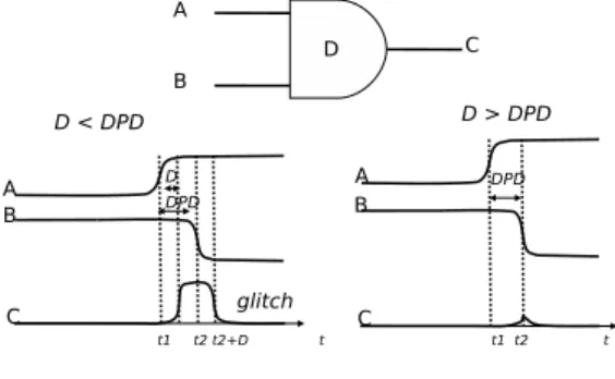
Glitch filtering approach was first proposed in [2]. The basic idea is to adjust the inertial delay of the gate, where glitch can be generated, to be greater than the differential path delay (DPD) of its input signals. Figure 1 illustrates this technique. The principle is simple : the transition of input signal A to logic state 1, will start the charging of output signal C. When the delay of the gate is smaller than DPD, the output will found enough time to be completely charged before being dicharged
due to the change of input signal B. Suppose now that the delay of the gate is increased by a factor DPD. Normally, the output will be at logic state 1 at time t1+D+DPD=t2+D. But, the change of input signal B to logic state 0, will start the discharge phase of output signal at time t2. Since the output is not being charged yet, the glitch will be filtered and the output remains at logic state 0 all the time.
Figure 1. Glitch filtering approach.
This technique may increase the overall delay of the circuit. For instance, consider the AND gate, with two rising transi-tions in its inputs. The output will be at the desired logic state after t+D, where t is the latest arrival time of input signals and D is the delay of the gate. Obviously, if the delay of the gate increases, the output will be delayed by a factor corresponding to the delay increase.
III. HAZARD FILTERING BY THRESHOLD VOLTAGE VARIATION
In this paper, we develop a new technique for hazard filtering based on threshold voltage variation.
The idea is by reason to the relation between the delay of a gate and threshold voltage that can be expressed as [9]:
tpd= CLVdd Id = CLVddLef f µCoxWef f(Vgs− Vth)α (1) where Vgs and Vth are respectively the gate-source voltage and the threshold voltage of the transistor, µ is the mobility, Cox is the oxide capacitance and α is the velocity saturation index. Lef f and Wef f are respectively the channel length and width of the transistor and CLis the equivalent capacitance of internal parasitic capacitances that consume the same power. The variation of the gate propagation delay resulting from a threshold voltage variation can be given in Equation 2 by diffrentiating Equation 1 with respect to Vth.
∆tpd=
α∆Vth Vgs− Vth
.tpd0 (2)
Where tpd0 is the original gate delay without Vth variation. The idea of our technique exploits this relation. It consists to adjust the threshold voltage in order to increase the delay of the desired gate by an optimal factor that achieve glitch energy savings while maintaining a certain performance requirement
on the overall circuit delay.
To achieve multiple threshold voltage, different techniques can be used. In [10], authors discuss these techniques. Some of them are integrated in the fabrication process like ion implantation or oxide thicknesses (tox) variation. The others, like multiple channel length setting or adaptive body biasing technique can be used by the designer in the transistor level. Transistor length variation increases gate’s capacitances which induce more power consumption. Thus, in this paper, we will use adaptive body biasing technique to achieve high threshold voltage. It’s a well known technique used for leakage energy reduction [6]. This technique consist to apply a voltage between the source and the bulk of the transistor that influence threshold voltage value. In fact, in BSIM4 model [11], the threshold voltage of a MOSFET can be expressed as follows:
Vth= Vth0+ γp2φF+ Vsb−p2φf (3)
Where Vth0 is the threshold voltage at zero substrate bias, φF is the Fermi potential, γ is the body bias coefficient and Vsb is the source-bulk voltage.
A variation in the source-bulk voltage results in a threshold voltage change by a factor of : γ√2φF+ Vsb−p2φf. This is especially used to increase threshold voltage by reverse biasing source to bulk junction [12].
Since this technique require a triple well process, we are aware that achieved energy savings will be at the expense of a certain area increase.
Figure 2 shows the variation of threshold voltage for a standard and a high threshold voltage low power (SVTLP and HVTLP) NMOS transistor resulting from a Vbsvariation.
0,2 0,4 0,6 0,8 1 1,2 1,4 1,6 1,8 2 2,2 0.73 0.85 0.9 0.58 V sb(V) VT H (V) HVTLP SVTLP
Figure 2. Threshold voltage variation for SVTLP and HVTLP NMOS transistors as function of Vsb.
As we can see, a reverse bias of about 0.5V results in an increase of threshold voltage by about 90 mV. Since transistor models don’t take into account a Vbs variation beyond Vdd + 10%, a maximum reverse biasing of 1.32V is allowed. A marge of 0.27V raging from 0.58V to 0.85V is possible.
IV. OPTIMIZATIONPROCEDURE FOR GLITCH POWER REDUCTION
In this section a motivation example for glitch filtering applying adaptive body biasing technique is presented. The proposed algorithm is then described and experimental results are shown.
A. Motivation Example
Consider the cicruit with a glitch formation shown in figure 3. Glitches appear due to the difference of input arrival times of the AND gate. As mentioned in section II, To eliminate glitches, threshold voltage will be adjusted by reverse biasing source to bulk junction.
Figure 3. Circuit with glitch formation.
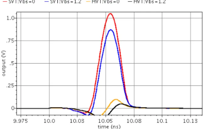
Spice simulations are carried out in 65nm process.
Figure 4 shows the output of the AND gate for different thresh-old voltages achieved using SVTLP and HVTLP transistors with and without substrate biasing. Here, the Vbs represent the value of the bulk-source voltage of PMOS transistors and the source-bulk voltage of NMOS ones.
Figure 4. Output voltage waveforms for different threshold voltages.
One can observe that, as expected, the magnitude of glitch is decreasing with threshold voltage increase.
Table I compares the original circuit and the modified one where HVTLP transistors and a substrate bias of 1.2V is used. We conclude that a total and leakage energy savings of up to 40% can be achieved at the expense of delay increase. For applications whose speed requirements are not stringent,
Table I
ENERGY REDUCTION AND DELAY PENALTY OF PROPOSED GLITCH REDUCTION METHOD APPLIED TO THE CIRCUIT IN FIGURE3.
original modified
Total-Energy(fJ) 4.76 2.85
Leakage-Energy(fJ) 7.99e-3 4.61e-3
Delay(ps) 74.8 107.8
Total-Energy-reduction(%) x 40
Leakage-Energy-reduction(%) x 42
Delay-increase (%) x 44
Energy-Delay-Product(psxfJ) 356.04 307.23
like biomedical devices, sensor networks and radio frequency identification (RFID) [13], delay of the circuit can be further and further increased as long as it achieves energy savings. But this is not generally the case : given as a constraint parameter, delay has been always a major concern for digital circuit designers.
B. Proposed algorithm
We develop an algorithm that modify the netlist of a logic circuit to have a glitch free one that still maintain a given circuit delay performance.
The proposed algorithm makes a bottom up analysis of the circuit : it starts at the primary inputs to finish at the output nodes. It effects a threshold voltage adjustement that may increase the overall circuit delay by a permitted amount calculated as the difference of the delay required and the critical path delay of the circuit without any modification. Effectively, this algorithm searches for an eventual glitch appearance by examining the differential path delay (DPD) of input signals of each gate in the circuit. For each glitchy gate, the highest threshold voltage achieved by using High Threshold Voltage Low Power (HVTLP) transistors with a substrate bias of 1.2V, is used. Then, if the critical path delay still maintain the delay requirements, the algorithm moves to the next gate. Else, the threshold voltage is regulated until the delay constraints are conserved.
The glitch may not be totally filtered, but its magnitude will be reduced which reduce the energy consumed as shown in section IV-A . For the case of a large DPD such that the glitch will be a complete transition with a width W, increasing threshold voltage will not reduce the energy consumed until W will be 0. Even so, the proposed algorithm achieve energy savings since high threshold voltage will significantly reduce leakage currents.
As using high threshold voltage reduce the leakage energy consumed, the circuit can be further optimized using the algorithm for non-glitchy gates.
To apply our algorithm the arrival times of input signals should be computed for all the gates of the circuit. The proposed algorithm is given in figure 5.
C. Experimental Results
The proposed algorithm has been tested on C17 and C432 ISCAS’85 benchmark circuits for different values of delay constraints.
{
Glitch_Reduction_by_threshold_voltage_variation_ algorithm (Circuit_netlist) Compute the inputs arrival time (ti) for each gate;
For each gate Gi { If |t1 − t2 | # 0 : { Gi=Gate−modif(delay_constraints,Gi) } } } Gate−modif(delay_constraints,gate) {For each transistor in the gate
{ transistors=HVTLP,Vbs=1.2 delay_verif=critical−path−delay−verif(delay_constraints,circuit_netlist) if !delay_verif {transistors=HVTLP,Vbs=0 delay_verif=critical−path−delay−verif(delay_constraints,circuit_netlist) } if !delay_verif {transistors=SVTLP delay_verif=critical−path−delay−verif(delay_constraints,circuit_netlist) } } } critical−path−delay−verif(delay_constraints,circuit_netlist) {if critical_path_delay > delay_constraints { return False Else return True } }
Figure 5. Threshold voltage variation algorithm to reduce glitches.
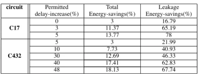
For simulation, 1000 random input vectors have been applied for each circuit. The results are shown in tableII.
Table II
TOTAL AND LEAKAGE ENERGY SAVINGS OFISCAS’85BENCHMARK CIRCUITS WITH DIFFERENT DELAY CONSTRAINTS
circuit Permitted Total Leakage
delay-increase(%) Energy-savings(%) Energy-savings(%)
0 3 16.79 C17 3 11.37 65.19 5 13.77 78 5 3 21.99 10 7.73 40.93 C432 30 12.69 46.33 40 17.41 62.83 48 18.13 67.74
The results show a significant energy savings after the algo-rithm has been applied.
We observe that for C17 circuit, we can even achieve energy savings without any increase in the circuit delay.
As expected the less the delay constraints are stringent the more the energy savings we can achieve.
Unlike others glitch reduction techniques, our technique do not adds an extra energy that reduce the achievable energy savings.
V. CONCLUSION
We describe an optimization technique for glitch power reduction based on threshold voltage variation. The idea is
to adjust threshold voltage of specific transistors of gates with eventual glitch appearance in order to eliminate spurious transitions and hence achieve energy savings.
We develop an algorithm that modifies a circuit netlist to have a glitch free one that still maintain the delay performance required. A total energy savings of 14% and a leakage energy savings of 78% at the expense of just 5% of delay increase is achieved applying our method to C17 benchmark circuit.
REFERENCES
[1] T. Raja, V. Agrawal, and M. Bushnell, “Variable input delay CMOS logic for low power design,” 2005.
[2] V. Agrawal, “Low-power design by hazard filtering,” vlsid, p. 193, 1997. [3] S. Kim, J. Kim, and S.-Y. Hwang, “New path balancing algorithm for glitch power reduction,” Circuits, Devices and Systems, IEE Proceedings
-, vol. 148, no. 3, pp. 151 –156, jun. 2001.
[4] A. Wroblewski, C. Schimpfle, and J. Nossek, “Automated transistor sizing algorithm for minimizing spurious switching activities in CMOS circuits,” in The 2000 IEEE International Symposium on Circuits and
Systems, 2000. Proceedings. ISCAS 2000 Geneva, vol. 3, 2000.
[5] T. Mudge, K. Flautner, D. Blaauw, and S. Martin, “Combined dynamic voltage scaling and adaptive body biasing for lower power micropro-cessors under dynamic workloads,” in iccad. IEEE/ACM, 2002, pp. 721–725.
[6] A. Agarwal, C. Kim, S. Mukhopadhyay, and K. Roy, “Leakage in nano-scale technologies: mechanisms, impact and design considerations,” in
Proceedings of the 41st annual Design Automation Conference. ACM,
2004, pp. 6–11.
[7] L. Wei, Z. Chen, K. Roy, M. Johnson, Y. Ye, and V. De, “Design and optimization of dual-threshold circuits for low-voltage low-power applications,” Very Large Scale Integration (VLSI) Systems, IEEE
Trans-actions on, vol. 7, no. 1, pp. 16–24, 1999.
[8] K. Yeo and K. Roy, Low voltage, low power VLSI subsystems. McGraw-Hill Professional, 2005.
[9] H. Luo, Y. Wang, K. He, R. Luo, H. Yang, and Y. Xie, “A novel gate-level NBTI delay degradation model with stacking effect,” Integrated
Circuit and System Design. Power and Timing Modeling, Optimization and Simulation, pp. 160–170, 2007.
[10] L. Wei, K. Roy, and V. De, “Low voltage low power CMOS design techniques for deep submicron ICs,” in Proceedings of the 13th
Inter-national Conference on VLSI Design. IEEE Computer Society, 2000,
p. 24.
[11] X. Xi, M. Dunga, J. He, W. Liu, K. Cao, X. Jin, J. Ou, M. Chan, A. Niknejad, and C. Hu, “BSIM4. 3.0 MOSFET Model User; s Manual,”
University of California, Berkeley, 2003.
[12] K. Layton, “Low-Voltage Analog CMOS Architectures and Design Methods,” Ph.D. dissertation, Citeseer, 2007.
[13] D. Bol, R. Ambroise, D. Flandre, and J. Legat, “Interests and limita-tions of technology scaling for subthreshold logic,” Very Large Scale
Integration (VLSI) Systems, IEEE Transactions on, vol. 17, no. 10, pp.