To link to this article : DOI: 10.1051/epjap/2013130080
URL : http://dx.doi.org/10.1051/epjap/2013130080
O
pen
A
rchive
T
oulouse
A
rchive
O
uverte (
OATAO
)
OATAO is an open access repository that collects the work of Toulouse researchers and
makes it freely available over the web where possible.
This is an author-deposited version published in:
http://oatao.univ-toulouse.fr/
Eprints ID: 16524
To cite this version: Bonnin, Xavier and Piquet, Hubert and Naudé, Nicolas and
Chérif Bouzidi, Mohamed and Gherardi, Nicolas and Blaquière, Jean-Marc
Design of a current converter to maximize the power into homogeneous
dielectric barrier discharge (DBD) devices. (2013) European Physical Journal:
Applied Physics, vol. 64 (n° 1). pp. 10901. ISSN 1286-0042
Any correspondence concerning this service should be sent to the repository administrator:
Design of a current converter to maximize the power
into homogeneous dielectric barrier discharge (DBD) devices
Xavier Bonnin1,2,a, Hubert Piquet1,2, Nicolas Naud´e1,2, Mohamed Ch´erif Bouzidi1,2, Nicolas Gherardi1,2,
and Jean-Marc Blaqui`ere1,2
1 Universit´e de Toulouse; INPT, UPS; LAPLACE (Laboratoire Plasma et Conversion d’ ´Energie);
ENSEEIHT, 2 rue Charles Camichel, BP 7122, 31071 Toulouse cedex 7, France
2 CNRS; LAPLACE, 31071 Toulouse, France
Abstract. This paper proposes a design approach of an electrical power supply intended to offer an espe-cially well-suited supply mode, through the efficient control of the current injected into a DBD setup. The proposed topology is aimed at controlling the operating point of the electrical discharge, thereby allowing favoring the homogeneous regime, and maximizing the electrical power injected into the plasma. The power supply structure is designed on the basis of causality criteria and of an analytical analysis of the electrical waveforms, which are derived from an equivalent circuit model of the DBD. Design issues of this electrical generator are detailed and experimental analysis of its operation, together with actual performances are presented. A very good agreement is obtained by comparing simulation and experiments. Effective ability to control the power transfers by means of its two degrees of freedom (current magnitude and frequency) is highlighted.
1 Introduction
Dielectric barrier discharges (DBDs) are nowadays exten-sively used to achieve the generation of cold plasmas at atmospheric pressure [1,2]; the dielectric barriers installed between the metallic electrodes of an AC discharge incor-porate two main advantages: they maintain the plasma in the non-equilibrium regime and help distribute the mi-crodischarges normally generated at high pressure over the entire electrode surface. Moreover it has been shown that in specific conditions, perfectly homogeneous discharges can be generated using DBDs [3]. These attributes are highly demanded in numerous processes, especially when relatively low temperatures are required, when the area to be affected by the effects of the plasma are large and when the costs associated with sophisticated vacuum units have to be avoided. Industrial applications of DBDs are spread out to various industrial domains, such as surface treatment [4–6], decontamination [7], semiconductor fab-rication, lighting – especially UV rays generation [8] by means of DBD excimer lamps. Most of the time, efficiency criterion concerning the industrial process favors the in-jection of a maximized power. However, and in partic-ular in the domain of surface treatments, the reliability of the process requires an accurate control of the
elec-a e-mail: [email protected]
trical power injected into the plasma, which in a second step defines the operating conditions of the discharge and thus the discharge regime (homogeneous or filamentary). Indeed, increasing the discharge power can result in mi-crodischarges, which are strongly non-uniform and in some cases are not suitable for the deposition of smooth thin film without defects. As a contribution to the satisfaction of these needs, this paper proposes a design approach of an electrical power supply intended to offer an especially well-suited supply mode, through the efficient control of the current injected into the DBD setup. In homogeneous DBDs generated in nitrogen atmosphere, the discharge power is in fact limited due to the limitation of the slope of the voltage versus time and the maximal discharge cur-rent [9]. Thus, in the case of sinusoidal excitation, the amplitude and the frequency of the applied voltage that allows the homogeneous discharge regime are limited. A solution to increase the discharge power is to limit the cur-rent and to increase the discharge duration. This could be realized using a square-wave current inverter source [10].
Hence, in Section2, the authors establish the merits of such current source generators [11]: on the basis of a clas-sical electrical model of the DBD [12], analytical calcula-tions are carried out and are used to compare a classical sinus voltage generator and a square shaped current source (the solution which is detailed in this paper); Section3is dedicated to the design of such a square shaped current
source: an innovative topology is proposed and the dimen-sioning of its components is achieved. A special attention is paid to the step up transformer and the effects of its parasitic elements (leakage inductance, windings capaci-tances) are analyzed in details. Experiments carried on a prototype designed according to the previously defined relationships are finally proposed: they validate the ex-pected performances detailed in Section2and the analysis concerning the transformers parasitic elements.
2 Supplying a DBD device with a current
controlled power supply
In this section, we show that controlling the injected cur-rent allows to increase the injected power in a DBD device. 2.1 The electrical behavior of a DBD device
The particularity of a Townsend regime is that the voltage is almost constant, equal to ±Vth, where Vthis the
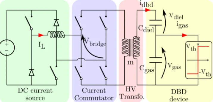
thresh-old voltage, whatever the current when the discharge is established (Fig.1) [13]. The gas volume is delimited by two parallels electrodes covered by dielectrics, thus ca-pacitive effects should be considered. These statements lead to the electrical model of the discharge presented Figure 2 [12]. Cgas and Cdiel are the equivalent
capaci-tors of the gas and the solid dielectric, respectively [9,10]. Their values are calculated assuming that the discharge section is equal to the entire electrode area. idbd − igas
is the displacement current which does not produce any power. The threshold device represents the static behavior of the gas in the Townsend zone, presented in Figure 1. The current passing through this device is called the dis-charge current igas(t) which is responsible for power
dis-sipation. Cdielrepresents the serial capacitance of the
lat-ter. Due to the presence of dielectric barrier, idbd has to
be such as ⟨idbd⟩T = 0, where ⟨·⟩T designates the average
value calculated over a time interval of length T , being T the operating period.
Current (logscale, arbitrary units)
Voltage (arbitrary units)
Vth Arc Normal glow discharge Townsend discharge Subnormal glow discharge Abnormal glow discharge
Fig. 1. Voltage-current characteristics of electrical discharge in gas at low pressure, with two planar electrodes.
Fig. 2. Simple electrical behavioral model of a DBD device.
-6 -4 -2 0 2 4 6 0 0.05 0.1 0.15 0.2 0.25 0.3 0.35 0.4-9 -6 -3 0 3 6 9
Voltage (kV) Current (mA)
Time (ms) V(t) Vgas(t) -4 -2 0 2 4 6 i dbd(t) igas(t)
Fig. 3. Shape of V (t), Vgas(t), idbd(t) and igas(t) with a
5 kV/5 kHz sinusoidal voltage source. Cgas = 10 pF, Cdiel =
70 pF and Vth= 3500 V.
2.2 Effective control of the operating point in the DBD device
2.2.1 With an AC voltage power supply
Considering the previously described circuit in Figure 2 we can see that the discharge current in the gas is given by ⎧ ⎨ ⎩ igas(t) = Cdiel dV dt discharge ON igas(t) = 0 discharge OFF
, (1) and the gas voltage by
⎧ ⎨ ⎩ Vgas(t) = Vth discharge ON Vgas(t) = Cdiel Cdiel+ Cgas V (t) discharge OFF , (2) where V (t) is the voltage across the DBD device. Numeri-cal simulation leads to the waveforms plotted on Figure3. Assuming that V (t) = ˆV cos(2πf t) and assuming that the gas changes from OFF state to ON state when the gas voltage reaches ±Vth, and changes from ON state to OFF
state when the discharge current vanishes (so, when the voltage source reaches an extremum) we find
P = 4f CdielVthVˆ $ 1 −$1 + Cgas Cdiel %V th ˆ V % , (3) where P is the mean injected power transferred to the DBD device. It is shown in (3) that the injected power
depends on both the frequency and the amplitude of the applied voltage which is consistent with experimental mea-surements. We note that a necessary condition to cre-ate power is that the amplitude of the applied voltage is greater than (1 + Cgas/Cdiel)Vth to allow the discharge
ignition. Moreover, we note that the DBD device has a “instantaneous voltage source” behavior since it is a ca-pacitive load. It means that the current in such a load can not be precisely controlled if supplied by a voltage source because it depends on the derivatives of the voltage ap-plied (and so on its fast variations). Causality rules lead us to control the current injected in the load, letting the voltage being imposed by the DBD device behavior. 2.2.2 With an AC rectangular current power supply
Waveforms and power transferred. Whatever the current shape, we find that
& i
gas(t) = idbd(t),
Vgas(t) = ±Vth,
(4) when the discharge is “ON” and
⎧ ⎪ ⎨ ⎪ ⎩ igas(t) = 0, Vgas(t) = Vgas(t0) + 1 Cgas ( t t0 idbd(τ) dτ, (5) when the discharge is “OFF”, idbd(t) is the current flowing
through the DBD device. For latter, we assume that the electrical supply presented in Figure 2 is a squarewave current source which frequency is f. Therefore we have idbd(t) = ±IDC. The theoretical waveforms of Vgas(t) and
igas(t) are plotted Figure 4. When the current changes
Fig. 4. Shape of V (t), Vgas(t), idbd(t) and igas(t).
from −IDCto +IDCthe operation can be decomposed in
two sequences [10]:
– When the discharge is in the “OFF” state, the gas voltage is growing up from −Vth to +Vth with a slope
IDC/Cgas according to (5). During this time interval,
no usable power is transferred into the plasma process, so the conduction current igasis zero. The duration τ
of this sequence is given by τ = 2VthCgas
IDC
. (6)
During this time interval, the transferred energy W is stored into Cgas. The latter takes the same value:
W = 1/2CgasVth2, (7)
at the beginning and at the end of τ time interval, and is null when Vgashas a zero value.
– When the gas voltage reaches Vth, the discharges turns
in the “ON” state and the current through the DBD device transfers power into the process; the displace-ment current is close to 0 (under the assumption that the gas voltage remains constant during the time in-terval during which the discharge is “ON”, then the displacement current is null). So, we have
Vgas= Vth and iCgas = 0.
The operating sequences are the same when the cur-rent idbd changes from +IDC to −IDC. . . Therefore, the
mean power transferred into the plasma process is given by P = 2f ( 1 2f 2VthCgas IDC IDCVthdτ, = VthIDC $ 1 −4VthCgasf IDC % , = VthIDC(1 − 2τf) , = VthIDC(1 − x) , (8)
where f is the operating frequency, and τ is given by (6). In order to simplify the notations the normalized variables r = Cgas/Cdiel and x = 4VthCgasf /IDC = 2τf has been
introduced.
2τf shows the normalized time to invert the polarity of the Vgas voltage and to change its value from −Vth to
Vth under the current IDC by one half-period.
Consider-ing the followConsider-ing usual orders of magnitude x is negligible compared to one if
– the operating frequency is in the range of several kilohertz,
– the discharge current density is higher than 1 mA/cm2,
which is a typical operating condition in nitrogen di-electric barriers controlled discharge,
– the gas gap is about few millimeters.
It proves that the injected power can be accurately ad-justed with a current controlled power supply since, ac-cording to (8) and the previous assumptions, P ≈ VthIDC.
Maximum voltage. One important quantity for designing such a current source with actual power electronics com-ponents is the operating voltage. This value can be calcu-lated by integrating the current flowing through Cdieland
the gas, considering that the mean value of Cdiel voltage
is zero. We find Vmax= ) 1 + r x * Vth. (9)
Typical value can be calculated considering that r is vary-ing from 0.1 to 1 and x is about 0.01. We can see that the voltage can easily exceed several tens of kilovolts. Thereby, in order to accommodate with current power electronics components features, a high voltage transformer should be included in the design of this power converter. Inser-tion of a transformer leads to add its parasitic elements in the designing process. The quantities previously calcu-lated (power, maximum voltage) should be a bit different from these given in (8) and (9). The way parasitic elements affect the waveforms is studied in Section3.4.
3 Design of a rectangular current source
In this section we study the implementation of an AC rec-tangular current controlled power supply. We first develop considerations concerning the architecture and the design of such a generator. In a second step, we focus on the par-asitic elements of the high voltage transformer and their effects on the waveforms and the performances. Demon-strations of the following equations can be found in [14]. Important elements from the specification for the design are remembered here:
– The designed generator is intended to be used for the research of the best suited supplying conditions, in order to maximize the electrical power injected into the plasma, while favoring the most homogeneous be-havior of the plasma. In this scope a 5–15 kHz range has been selected for the frequency since it has proved to provide homogeneous discharges in nitrogen at at-mospheric pressure with an AC voltage source supply. – The maximal current density in the DBD device is about few mA/cm2. For experimental validations, a
maximal current of 10 mA/cm2is chosen and a 9 cm2
sample could be used: so we have to generate a current about 90 mA [3].
– The voltage we have to deal with is about tens of kilovolts since the gas threshold voltage is about 3500 volts (9) [13].
3.1 Some design considerations
The main matter is to design a low-current square wave-form power supply sustaining high voltage. A cascaded topology has been chosen; it includes two power convert-ers (Fig.5).
Fig. 5. A two-stages cascaded power converter to generate square waveform current.
– The first one is a tunable regulated DC current source. – The second one allows to transform the DC current
into an alternative square waveform current.
Although the high voltage transformer design is a very important aspect because of its parasitic elements, as de-veloped in Section 3.4, its design is not treated in this paper.
Care must be taken when sizing the first stage com-ponent since the current ripple have to be quite low in order to generate a well suited current waveform. A four switches bridge is needed to produce the square shape current. The input voltage of the latter (Vbridgeon Fig.5)
exhibits a sawtooth bidirectional waveform (Fig. 6b). So the DC current is controlled by means of a two quadrants chopper.
The switching frequency of the commutator depends on the plasma process specifications and should be tunable. It has been chosen to carry experimental investi-gations in the 5–15 kHz range. It does not need feedback-control since the commutator must only ensure that its duty cycle is 50% (that can be performed in an open-loop control with a well-designed modulator). Neverthe-less, a DC component would bias the transformer’s core and make it going on saturation if the duty cycle is not well controlled, drastically reducing the coupling between the primary and the secondary winding.
(a) (b) (c)
Fig. 6. Theoretical waveforms and commutator’s switches characteristics. Vbridge (gray), IK (red), VK (blue). Figure (a)
3.2 The commutator: synthesis of semiconductor switches
Theoretical waveforms concerning a commutator’s switch Figure 6a are presented in Figure 6b. According to these waveforms, the upper-left switch static and dynamic char-acteristics are defined on Figure 6c. The same study car-ried out on the other commutator switches shows that they behave the same way.
Static characteristics are such that the switch should sustain positive and negative voltage, and conduct only positive current that confirms the use of 3-segments power switches (Fig. 6c). Analysis of the switchings show that it is
– turned on under a positive voltage conducting a posi-tive current meaning a controlled turn on,
– turned off because of a zero crossing of its current (soft switching).
We recognize the behavior of a thyristor-like switch. Power synthesized thyristors such as presented in [15] should be used, because of the high switching frequency since cur-rent thyristor technology is not suitable for more than a few kHz.
3.3 The current source
The first stage of the power converter is made of a full-bridge topology. We can notice that basic designing rules would have led to work with a half-bridge topology (say a classical Buck step down chopper). Indeed, the current flowing through the switches is positive and the voltage that switches have to deal with is positive too. The matter is that even if the mean voltage drop seen after the induc-tance is positive (⟨Vbridge⟩ > 0), it varies between negative
and positive bounds (Fig.6b). When it is negative, there is no switch configuration that would allow to decrease IL value. Therefore, this leads to a temporary loss of the
current value control during the time Vbridge is negative.
Moreover, considering that the mean value of this volt-age should be quite low compared to input voltvolt-age one, the duty cycle should be often close to zero which leads to technical problems because the ON time could be of the same order of magnitude as typical MOSFET switch-ing time. Furthermore, another advantage of choosswitch-ing a full-bridge topology is that it leads to work with a duty-cycle varying around a value slightly higher than 0.5. The features of this stage is to ensure the constancy of the inductance current value (called IL on Fig. 5) although
the output voltage Vbridge varies quickly. This
specifica-tion can be honored by a fast control law as current-mode one. Current mode control leads underlying problem such as loss of stability when the ordered duty-cycle is above 50%. Ramp-compensation technique [16] has been used to overcome this problem.
The first stage’s power inductor sizing. The value of L is chosen according to the well-known formula in the case
Trapezoidal current source m
Cp Cdiel + mI- dc + I- dc idbd iCp igas Cgas Vth -Vth
Fig. 7. Theoretical scheme taking into account the parasitic effects within the high voltage transformer.
of a two quadrants chopper: ∆ILmax=
Vin
2Lf. (10) Thus, if Vin≈ 300 V, f = 40 kHz, mIDC= 15 A and if we
want ∆ILto be lower than 5% of ⟨IL⟩, we can choose L ≈
10 mH. The core could be Fe-Si laminated based because the high frequency core losses are quite low because of the selected low value of ∆IL.
3.4 Influence of transformer’s parasitic elements Actual waveforms are quite different from that presented in Figure 4. Many parasitic effects due to the presence of the high voltage transformer affect the waveforms. A general scheme taking into account all these effects is pre-sented Figure7. Lµ is the magnetizing inductance of the
transformer, Lℓ is the leakage inductance and Cp serve
at modeling the capacitive effects in the transformer. We study the three main effects: the capacitive effects in Section3.4.1, the leakage inductance effect in Section3.4.2 and the magnetizing inductance effect in Section 3.4.3.
3.4.1 Parasitic capacitance
The current measured after the secondary winding is not rectangular because of the transformer capacitive parasitic effects. The consequence of capacitive effect is that a frac-tion of the injected primary current is derived through the dielectrics constituting the high-voltage transformer. Lo-cating actual capacitive coupling is complex. However sim-plified analytical method convenient for modeling DBD device high-voltage transformers and design rules in order to minimize stray capacitance effects are proposed in [17]. However, we can consider that the leading effect can be represented as a capacitor connected between the trans-former secondary winding terminals.
Considering the scheme Figure 7 and neglecting the other parasitic effects leads to write
idbd igas
+ I- DC
Fig. 8. Theoretical waveforms taking into account only the capacitive effects within the high voltage transformer.
⎧ ⎪ ⎪ ⎨ ⎪ ⎪ ⎩ idbd= ± Cdiel Cdiel+ Cp IDC discharge ON idbd= ± Ceq1 Ceq1+ CpIDC discharge OFF , (11) where Ceq1= CdielCgas/(Cdiel+ Cgas) and IDCis the
the-oretical rectangular waveform current amplitude we want to inject in the DBD. The general appearance of the wave-forms are sketched Figure8from (11) taking into account only the capacitive effects. The main effect is that the time the discharge is ON is diminished compared to Figure4.
Therefore the power transferred is diminished too. The ON time during a period is given by
tON= $ 1 − (1 + r)$1 + r′+r′ r % x% 1 f, (12) and the mean power transferred to the DBD device is given by P = 1 1 + r′ $ 1 −$1 + r′+r′ r % x % VthIDC, (13)
where r = Cgas/Cdiel, r′ = Cp/Cdiel, x = 4VthCgasf /IDC
and f is the switching frequency of the commutator. The experimental waveforms of Section4.2are obtained with a transformer which exhibits Cp≈100 pF stray capacitance.
The important influence Cp has on the performances of
the system is highlighted in P (x)/(VthIDC) plot Figure9:
Cp has to be minimized (r′ minimized) by well designing
the high-voltage transformer since the injected power P decreases as Cpincreases for the same operating points at
the primary side. Moreover, Vmax is decreased by factor
(1 + r′) giving
Vmax=
1 + r/x
1 + r′ Vth. (14)
It should be noticed that the way the transformer is grounded is an important aspect for the capacitive effects: the equivalent capacitance value strongly depends on that. In order to minimize its value, the ground connected to the magnetic core, should be also connected to the middle point of the secondary winding. This approach could not be always performed because it involves to work with two floating point, thus no electrode is actually connected to the ground. r' = 0 r' = 0.57 r' = 1.14 r' = 1.71 10-3 10-2 10-1 1 0.2 0.4 0.6 0.8 1 x Injected power diminishes as r' increases P Vth I DC
Fig. 9. Theoretical power plot versus x with r = 0.1 showing the influence of Cp(r′= Cp/Cdiel).
3.4.2 Leakage inductance
In addition to the capacitive effects, the leakage induc-tance (considered at the primary winding) influences the waveforms and the commutator behavior. Since power switches are synthesized thyristors their spontaneous blocking state could not occur until the leakage induc-tance current has not reached ±mIDC, where m is the
transformer ratio. Thus, reversing the current sign in the primary winding may take some time and steep transition can not be obtained and so the current waveform that can be generated at the primary winding has a trapezoidal shape instead of a square shape. When it is ordered that the primary current changes from +mIDC to −mIDC by
switching ON the two blocked switches of the commuta-tor, the voltage drop across the primary winding is about Vmax/m; see (9) for the Vmaxexpression. Thus, the leakage
inductance current has to change from +mIDCto −mIDC
under a voltage Vmax/m (we suppose that the voltage does
not change significantly during the transition). Thus, the time this transition takes is then given by
tt= 2m2 1 + r′ 1 + r/x LℓIDC Vth , (15) with the same notations as previously, where Lℓ is the
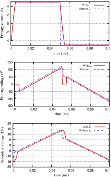
leakage inductance value. To illustrate, a comparison is made in Figure 10. Theoretically, the transition time should be tt= 4.12 µs using (15). Numerical simulations
gives tt ≈ 4.55 µs. The difference between these values
is due to the fact that the primary voltage is not really constant during the transition. We retain that (15) gives a good approximation of ttanyway. When sizing the high
voltage transformer, it must be ensured that the transition time can be neglected compared to the switching period. Therefore Lℓ should be such as
Lℓ≪ 1 + r/x 1 + r′ Vth 2m2f I DC . (16)
-4 -2 0 2 4 0 0.02 0.04 0.06 0.08 0.1 With Le Without Le With Le Without Le With Le Without Le time (ms)
Primary current (A)
-150 -100 -50 0 50 100 150 0 0.02 0.04 0.06 0.08 0.1 time (ms) Primary voltage (V) -20 -15 -10 -5 0 5 10 15 20 0 0.02 0.04 0.06 0.08 0.1 time (ms) Secondary voltage (kV)
Fig. 10. Influence of Lℓ. PSIM simulation with f = 10 kHz,
IL = 5 A, Cp = 0 pF, Cgas = 10 pF, Cdiel = 100 pF, Vth =
3500 V, m = 117 and Lℓ= 50 µH.
Actually, a well suited high voltage transfomer can sat-isfy the criterion (16) as long as the switching frequency is in a reasonable range (less than a few tens of kHz). 3.4.3 Magnetizing inductance
The role of the magnetizing inductance can be often ne-glected since its value can be well controlled when design-ing the high voltage transformer. Magnetizdesign-ing inductance sinks a 180 degree dephased current compared to idbd,
which slightly affects the current waveform (see experi-mental results in Sect. 4.2). Neglecting the effect of Lℓ,
but taking into account the capacitive effects, the max-imum value of the current absorbed by the magnetizing inductance is given by Iµmax= Vth mLµf $A x + Bx % , (17) where Lµis the magnetizing inductance (considered at the
primary winding side), Imax
µ is the maximum current that
flows through Lµ and the coefficients A, B are given by
A = r 8(1 + r′), B = 2rr ′+ 1 + 2r + 2r′ 8r(1 + r′) . (18) To ensure that the effect of Lµ can be neglected, care
must be taken to check that Imax
µ ≪ mIDCwhen
design-ing/choosing the high voltage transformer.
4 Implementation of the power converter
and experimental results
The DBD device is made of two 9 cm2 silver electrodes
pasted on 0.635 mm thickness Al2O3 dielectrics. The gas
gap is about 1 mm. Parameters values are Cgas≈ 10 pF,
Cdiel≈ 70 pF and Vth≈ 3.9 kV [9].
4.1 Implementation of the power converter
The power converter presented Figure5has been realized to conduct experimental campaigns in order to identify parameters which influence on the discharge behavior. The main characteristics are:
– It can provide a current IL (Fig. 5) up to 15 A (in
steady state) and work with an input voltage up to 400 V.
– The first stage switching frequency is fixed at 40 kHz, its inductance value is about 8 mH. The current IL is
tunable from 1 A to 15 A.
– The second stage switching frequency is tunable from 4 kHz to 17 kHz. The thyristor behavior is emulated by a MOSFET transistor in series with a diode, and an appropriate control law.
– The high voltage transformer we use exhibits a ratio of 155, a leakage inductance Lℓ of 18 µH, a magnetizing
inductance Lµ of 16 mH, and an equivalent parasitic
capacitance Cp of 100 pF.
4.2 Experimental results
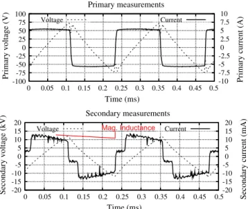
Results at 5 kHz and 10 kHz are provided on Figures11 and12.
– The magnetizing inductance’s effect is the change of the current shape at the secondary winding since a fraction of the injected current serves at magnetizing the transformer core.
– The leakage inductance make the current shape trape-zoidal. During this transition time, the measured volt-age drop across the primary winding of the power transformer vanishes since synthesized thyristors all are in the ON state (see Fig.12).
– The parasitic capacitance effect is more important at high frequencies. It delays the gas breakdown absorb-ing a fraction of the injected current (this fraction of current is not the same depending on whether the dis-charge is alight or not). Therefore the measured cur-rent is lower than that it was expected.
-100-75 -50 -25 0 25 50 75 100 0 0.05 0.1 0.15 0.2 0.25 0.3 0.35 0.4 0.45 0.5-10 -7.5 -5 -2.5 0 2.5 5 7.5 10
Primary voltage (V) Primary current (A)
Time (ms) Primary measurements Voltage Current -20 -15 -10-5 0 5 10 15 20 0 0.05 0.1 0.15 0.2 0.25 0.3 0.35 0.4 0.45 0.5-20 -15 -10 10 15 20
Secondary voltage (kV) Secondary current (mA)
Time (ms) Secondary measurements Voltage -50 5 Current Mag. Inductance
Fig. 11. Experimental results at 5 kHz (smoothed curves).
-75 -60 -45 -30 -150 15 30 45 60 75 0 0.025 0.05 0.075 0.1 0.125 0.15 0.175 0.2 0.225 0.25-15 -12 -9 -6 -3 0 3 6 9 12 15
Primary voltage (V) Primary current (A)
Time (ms) Primary measurements Voltage Current -12-9 -6 -30 3 6 9 12 0 0.025 0.05 0.075 0.1 0.125 0.15 0.175 0.2 0.225 0.25-36 -27 -18 -9 0 9 18 27 36
Secondary voltage (kV) Secondar
y current (mA) Time (ms) Secondary measurements Voltage Current Leakage Inductance Parasitic capacitance
Fig. 12. Experimental results at 10 kHz (smoothed curves).
5 Conclusion
In this paper, the arguments for selecting a current con-trolled generator with a rectangular shape, in order to increase the amount of power injected into a DBD, and to maintain in the same time the electrical discharge in the homogeneous regime, have been evoked. The classi-cal equivalent circuit of the DBD has shown to be of great interest in order to build the analytical relationships char-acterizing the electrical quantities of such a power supply. On this basis, an experimental setup has been designed and implemented. The effects of the parasitic elements of the step-up transformer inserted into the power trans-fer chain have been analyzed in details. The conclusions are clearly showing that the transformer is one of the key
components with respect to the effective control of the electrical power transferred into the gas, and that a great care has to be taken to control especially the parasitic capacitance as seen from the secondary winding, during the design of the latter. The proposed topology offers two degrees of freedom to control the operating condi-tions: the magnitude and the frequency of the rectangular current injected into the transformer. The output char-acteristics of the designed generator have been measured and are showing on the one hand a very good agreement with the expected theoretical ones, and on the other hand very promising performances, when compared with sim-ilar characteristics concerning a classical voltage source generator.
The authors are grateful to the French Midi-Pyr´en´ees region for its support (PHPA project).
References
1. U. Kogelschatz, Plasma Chem. Plasma Proc. 23, 1 (2003) 2. F. Massines, A. Rabehi, P. Decomps, R.B. Gadri, P. S´egur,
C. Mayoux, J. Appl. Phys. 83, 2950 (1998)
3. F. Massines, N. Gherardi, N. Naud´e, P. S´egur, Eur. Phys. J. Appl. Phys. 47, 22805 (2009)
4. F. Massines, G. Gouda, N. Gherardi, M. Duran, E. Croquesel, Plasma. Polym. 6, 35 (2001)
5. R. Seeb¨ock, H. Esrom, M. Charbonnier, M. Romand, U. Kogelschatz, Proceedings of the 7th International Confer-ence on Plasma Surface Engineering, Surf. Coat. Technol. 142–144, 455 (2001)
6. C. Zhang, T. Shao, K. Long, Y. Yu, J. Wang, D. Zhang, P. Yan, Y. Zhou, IEEE Trans. Plasma Sci. 38, 1517 (2010) 7. G. Vezzu, J.L. Lopez, A. Freilich, K.H. Becker, IEEE
Trans. Plasma Sci. 37, 890 (2009)
8. M. Lomaev, E. Sosnin, V. Tarasenko, D. Shits, V. Skakun, M. Erofeev, A. Lisenko, Instrum. Exp. Tech. 49, 595 (2006) 9. N. Naud´e, J.-P. Cambronne, N. Gherardi, F. Massines, J.
Phys. D: Appl. Phys. 38, 530 (2005)
10. S. Vongphouthone, H. Piquet, H. Foch, Eur. Phys. J. Appl. Phys. 15, 123 (2001)
11. R. D´ıez, H. Piquet, M. Cousineau, S. Bhosle, IEEE Trans. Ind. Electron. 59, 1912 (2012)
12. R. D´ıez, J.P. Salanne, H. Piquet, S. Bhosle, G. Zissis, Eur. Phys. J. Appl. Phys. 37, 307 (2007)
13. Y.P. Raizer, Gas Discharge Physics (Springer Verlag, Berlin, 1991)
14. X. Bonnin, Master’s thesis, INP Toulouse, ENSEEIHT, 2011
15. M. Cousineau, R. D´ıez, H. Piquet, O. Durrieu, IEEE Trans. Ind. Electron. 59, 1920 (2012)
16. C. Basso and ON-Semiconductor, Application note AND8029/D Ramp Compensation for NCP1200, Technical report, ON Semiconductor, 2001
17. X. Bonnin, H. Piquet, D. Florez, R. Diez, Designing the high voltage transformer of power supplies for dbd: windings arrangment to reduce the parasitic capacitive effects, in European conference on Power Electronics (EPE), 2013