This is an author-deposited version published in:
http://oatao.univ-toulouse.fr/
Eprints ID: 11450
To link to this article: DOI: 10.1016/j.crhy.2014.02.006
URL:
http://dx.doi.org/10.1016/j.crhy.2014.02.006
To cite this version:
Sokoloff, Jérôme and Pascal, Olivier and Callegari,
Thierry and Pascaud, Romain and Pizarro, Francisco and Liard, Laurent
and Lo, Juslan and Kallel, Asma Non-thermal plasma potentialities for
microwave device reconfigurability. (2014) Comptes Rendus Physique,
vol. 15 (n° 5). pp. 468-478. ISSN 1631-0705
O
pen
A
rchive
T
oulouse
A
rchive
O
uverte (
OATAO
)
OATAO is an open access repository that collects the work of Toulouse researchers and
makes it freely available over the web where possible.
Any correspondence concerning this service should be sent to the repository
administrator:
[email protected]
Electromagnetism / Électromagnétisme
Non-thermal plasma potentialities for microwave device
reconfigurability
Potentialités des plasmas froids pour la reconfigurabilité de dispositifs
micro-ondes
Jérôme Sokoloff
a,b,∗
, Olivier Pascal
a,b, Thierry Callegari
a,b, Romain Pascaud
c,
Francisco Pizarro
a,c, Laurent Liard
a,b, Juslan Lo
a,b, Asma Kallel
a,baUniversité de Toulouse, UPS-INPT LAPLACE, 118, route de Narbonne, Bât. 3R2, 31062 Toulouse cedex 9, France bLaboratoire Plasma et Conversion d’Énergie (LAPLACE), CNRS, 31000 Toulouse, France
cUniversité de Toulouse, ISAE DEOS, 10, avenue Édouard-Belin, BP 54032, 31055 Toulouse cedex 4, France
a r t i c l e
i n f o
a b s t r a c t
Keywords: Microwave Cold plasma Metamaterials Leaky wave Antenna Mots-clés : Micro-ondes Plasma froid Métamatériaux Onde de fuite AntenneThree examples of results achieved from cooperative works with microwave and plasma research groups in Toulouse (France) are presented in this paper. They are focused on the use of few non-thermal plasmas to make a microwave device reconfigurable. The relative permittivity of such a plasma medium can be tuned from unity to negative values. This special feature appears to be very attractive, although the electromagnetic losses are significant. The use of plasmas with planar waveguides and within metamaterials is discussed. In addition, the basic principles of a scanning antenna built with a leaky wave in a plasma layer are presented.
r é s u m é
Nous présentons dans ce papier trois exemples de travaux menés à Toulouse par des équipes issues des communautés micro-ondes et plasma. L’objectif est d’utiliser des plasmas froids pour rendre un dispositif micro-ondes reconfigurable. En effet, la permittivité relative du plasma peut être contrôlée et varier de l’unité jusqu’à des valeurs négatives. L’exploitation de cette propriété s’avère potentiellement très intéressante. En revanche, aux fréquences micro-ondes, les pertes électromagnétiques sont importantes. L’intégration de plasmas dans des structures planaires puis dans des métamatériaux est présentée. En complément, nous exposons le principe d’une antenne à balayage à onde de fuite utilisant un plasma.
*
Corresponding author.E-mail addresses:[email protected](J. Sokoloff),[email protected](O. Pascal),[email protected]
(T. Callegari),[email protected](R. Pascaud),[email protected](F. Pizarro),[email protected](L. Liard),
Fig. 1. Schematic of the inverted microstrip line. Fig. 1. Schéma de la ligne microruban inversée.
1. Introduction
Putting together more and more microwave functions in today systems leads to an increasing interest in the re-use of devices for several systems or sub-systems. As an example, the same filter is intended to switch between Wi-Fi and 3G modes in order to avoid multiple filters. Reconfigurability is then a way to make these systems more compact and efficient. Although they are not so easy to deal with, several strategies are developed with components like diodes[1], MEMS[2], liquid crystals[3], or ferrimagnetic materials[4]. Each of these technologies has its own advantages and drawbacks. This paper investigates the potential of an alternative solution for reconfigurability: the use of non-thermal plasmas.
Such plasmas exhibit remarkable properties regarding microwave propagation or reflection. They are well suited to high-power densities up to 1 MW
/
m2. Either the active volume or its permittivity can be tuned quickly, from the millisecond tothe nanosecond range with dedicated pre-ionization circuits. Nevertheless, their high microwave absorption, which can lead to insertion losses of several dB and even more, is often cited as a major concern. Actually, this property can be useful in some special cases.
Guided microwaves are well known to be very sensitive to whatever is put in their vicinity or added to the waveguide. Integrating plasma discharges without disturbing too much the wave then appears to be quite difficult. Encapsulating gas with controlled composition and pressure, designing appropriate electrodes that do not interfere with the wave are the challenges addressed here. Several talks, meetings and cooperative projects putting together both the plasma and microwave local communities were required to achieve the new ideas developed in this paper, which are gathered in three different parts.
First, we will see that having a realistic knowledge of the wave/plasma interaction is not so easy. It leads to design some specific measurement toolbox in order to quantify what is the effect of a microplasma on a wave travelling in a conventional microstrip inverted line. Second, we present an example of our works concerning the integration of localized plasmas within an Electromagnetic Band Gap (EBG) structure. The originality of this approach consists of few localized plasmas used as controllable defects. We show the case of metallic EBG structure in which anisotropy is driven by two plasma tubes. Finally, we briefly expose the concept and dimensioning of a leaky wave plasma antenna with beam scanning capabilities.
2. Getting realistic data about microwave/microplasma interaction
The wave/plasma interaction and its use is an old question. Since the design of radar duplexers and limiters in the late 1940s[5], papers regularly deal with this topic. More recently, a new interest for agile radar mirrors[6]or invisible RCS antennas (when off)[7]has been noticed. In the last few years, some theoretical results were also published concerning couplers[8]or antennas[9]in the context of the use of metamaterials.
Considering the simple fluid model of a plasma material, only the electron density and the collision frequency are required to describe the electromagnetic behaviour of the plasma. A Drude model[10]then gives the equivalent complex permittivity and makes it possible to simulate, by any conventional technique, a wave propagating through it. However, these two parameters appear not to be fully independent and almost related to the system producing the plasma discharge. Besides, this plasma discharge remains a complex inhomogeneous medium whose electron density spatial distribution is difficult to predict. As a consequence, we concluded that only the experimental characterization of a canonical configuration could help in the further design of more sophisticated microwave devices.
The proposed measurement device consists of a 50-
Ä
inverted microstrip line with a microplasma discharge in itscentre [11]. The microplasma discharge is in fact generated using a Micro-hollow Cathode Sustained Discharge (MCSD) configuration[12,13]. Such a configuration seems interesting because of its capability to produce very localized and stable microplasmas in a wide range of pressures. Moreover, it can be easily integrated in many planar waveguides. Note that the
Fig. 2. Split and cut views of the measurement device. Fig. 2. Vues éclatée et en coupe du dispositif de mesure.
Fig. 3. Picture of the measurement device. Fig. 3. Photo du dispositif de mesure.
inverted microstrip line has been selected keeping in mind that the possible expansion of the plasma in the active zone between the two conductors could lead to more significant interaction.
The microstrip inverted line of 50-
Ä
characteristic impedance is described inFig. 1. The centred hole is machined as a part of the MCSD configuration as well as the ground plane of the line (anode 1) which can be seen inFig. 2. Finally, this measurement device is inserted in a vacuum chamber where we can control the type of gas and its pressure as well as the DC power injected to the plasma discharge while measuring the S parameters of the inverted microstrip line. A picture of the final measurement device is shown inFig. 3where the plasma electrodes, the inverted microstrip line substrate, the RF ground plane and the SMA connectors can be seen in the glass vacuum chamber.As a result of such integration, the propagation through the line is expected to exhibit no reflection and full transmission when the plasma is off. When it is on, however, there will be more reflection and less transmission. On the one hand, both the magnitude and the phase of the measured S21 parameter will characterize the plasma effect on the transmitted wave. On the other hand, the measured S11 parameter will tell us about the reflected wave. Actually, one has to keep in mind that this full S parameter characterization is enough to further simulate the behaviour of a global microwave circuit with a conventional electromagnetic tool by associating one or more reconfigurable microdischarges with active or passive components (lines, junctions, inductors, capacitors, transistors
. . .
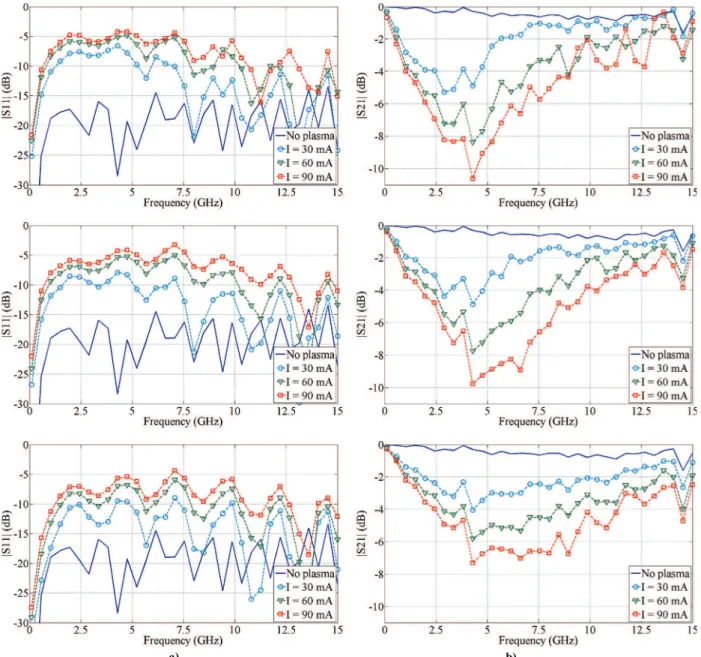
).Fig. 4a presents the measured S11 magnitude considering a gas made of 99% of neon and 1% of xenon at different pressures, namely 3.3 mbar, 13.3 mbar and 66.5 mbar. This gas has been chosen to maximize the electron density while minimizing the collision frequency.
Fig. 4. a) Measured S11 magnitude as a function of the frequency, of the DC current injected to the discharge and of the gas pressure (3.3 mbar, 13.3 mbar
and 66.5 mbar). b) Measured S21 magnitude as a function of the frequency, of the DC current injected to the discharge and of the gas pressure (3.3 mbar, 13.3 mbar and 66.5 mbar). For interpretation of references to colour, see the online version of this article.
Fig. 4. a) Amplitude du S11 en fonction de la fréquence, du courant continu injecté à la décharge et de la pression du gaz (3.3 mbar, 13.3 mbar and
66.5 mbar). b) Amplitude du S21 en fonction de la fréquence, du courant continu injecté à la décharge et de la pression du gaz (3.3 mbar, 13.3 mbar and 66.5 mbar). Pour l’interprétation des références faites à la couleur, voir la version en ligne de cet article.
First, note that this line is quite well matched over the whole frequency band with a S11 parameter lower than
−
15 dB when there is no plasma. Second, we notice a significant effect of the plasma discharge that tends to mismatch the trans-mission line. Differences up to 10 dB are then depicted on the S11 magnitude that points to an important effect of the microplasma on the wave. Considering the frequency, the highest effect appears to be in the middle of the presented band-width. The pressure here seems ineffective.Second and third sets of results concern both the magnitude (Fig. 4b) and phase (Fig. 5a) of the transmission coefficient, i.e. the S21 parameter. The latest is related to the phase with no plasma and then denoted as the phase difference.
Regarding the S21 magnitude, we notice that both the pressure and the frequency are of some importance. The good transmission of more than
−
1 dB without plasma is drastically reduced down to−
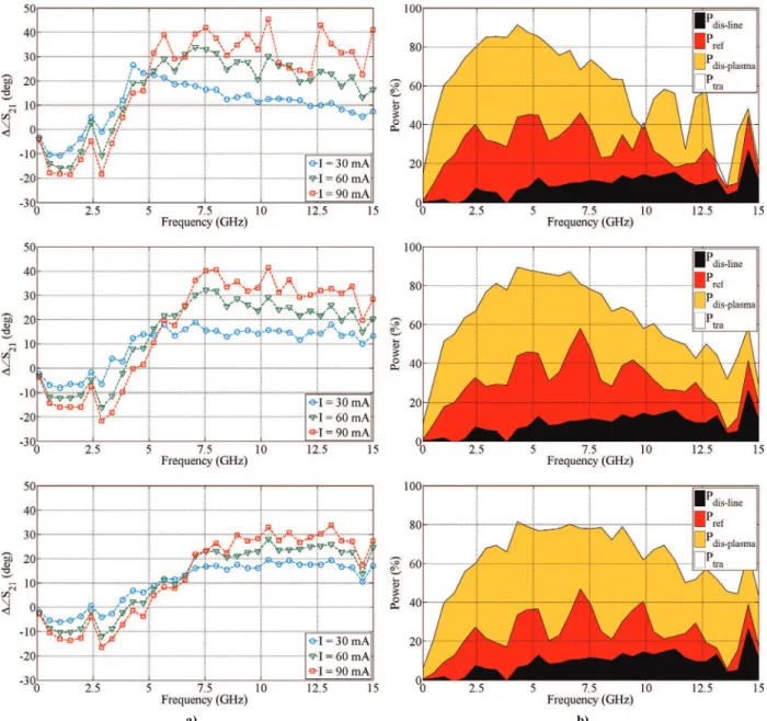
10 dB at its peak value. Both this value and its spectral localization are affected by the gas pressure. Lower pressure, here, leads to higher effects, while higher discharge currents increase the effect too. These remarks can be extended to the phase difference curves inFig. 5a. TheFig. 5. a) Measured S21 phase difference as a function of the frequency, of the DC current injected to the discharge and of the gas pressure (3.3 mbar,
13.3 mbar, and 66.5 mbar). b) Measured power balance as a function of the frequency and of the gas pressure (3.3 mbar, 13.3 mbar, and 66.5 mbar) for a DC current of 90 mA. For interpretation of references to colour, see the online version of this article.
Fig. 5. a) Mesure du déphasage relatif S21 en fonction de la fréquence, du courant continu injecté à la décharge et de la pression du gaz (3.3 mbar,
13.3 mbar et 66.5 mbar). b) Mesure du bilan de puissance en fonction de la fréquence et de la pression du gaz (3.3 mbar, 13.3 mbar and 66.5 mbar) pour un courant injecté à la décharge de 90 mA. Pour l’interprétation des références faites à la couleur, voir la version en ligne de cet article.
global variation of 40° peak is not very impressive, but when compared to the size in wavelength of the microdischarge (
λ
min/
15), it becomes more interesting, especially when some of these values are achieved in low-loss area (e.g., at 3.3 mbarand 14 GHz). Some other comments could focus on the sign inversion of the phase difference, which can be interpreted with respect to phase velocities lower or higher than the vacuum one (considering effective permittivity of the inverted line around 1). This is also an interesting property usually expected with plasmas.
Finally, we propose to deal with the power balance in order to have a special look on the plasma losses. Theoretically, the incident wave normalized power is reflected, transmitted, and/or dissipated. The first two contributions are easy to get considering the magnitudes of the S11 and S21 parameters. Assuming that the power dissipated in the line materials (both conductive and dielectric parts) remains unchanged whether the plasma is on or off, we can get the plasma absorbed power. Such graphs are depicted inFig. 5b.
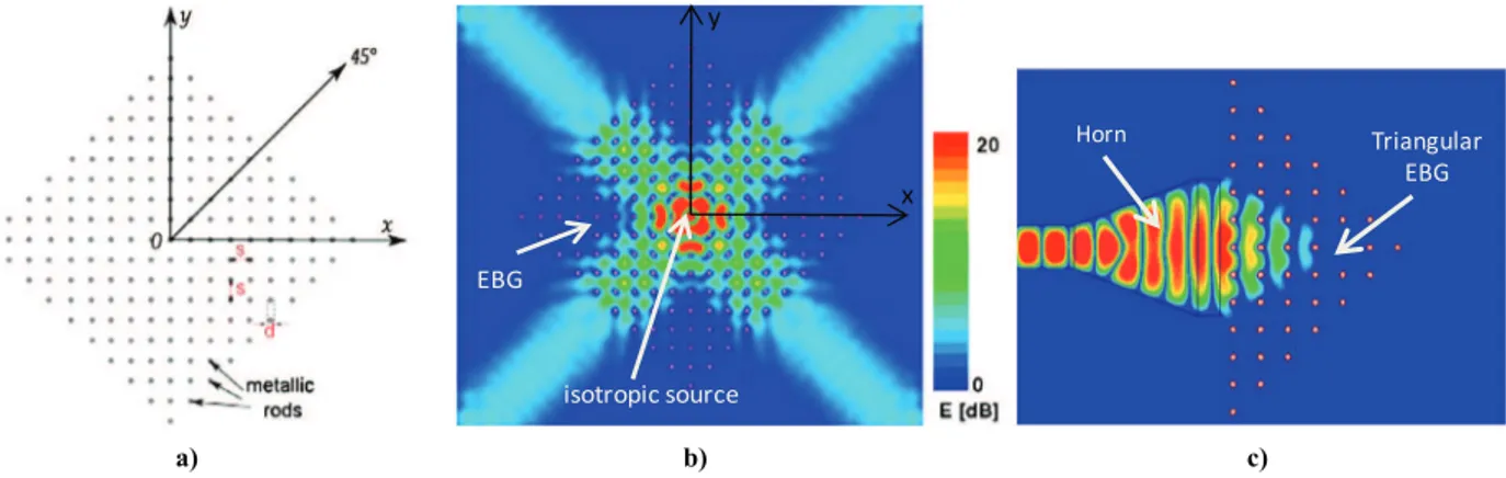
Fig. 6. (Colour online.) a) Metallic EBG structure. Rod diameter d=2 mm, lattice step size s=10 mm. b) Simulation of the electromagnetic field radiated by an isotropic source within the EBG structure at 18 GHz. c) Simulation of the triangular-shaped EBG structure illuminated by a specific horn at 18 GHz.
Fig. 6. (Couleur en ligne.) a) Structure BIE métallique. Diamètre des tiges d=2 mm, pas du réseau s=10 mm. b) Simulation du champ électromagnétique rayonné par une source isotrope dans la structure BIE à 18 GHz. c) Simulation de la structure BIE triangulaire éclairée par un cornet spécifique à 18 GHz.
On a 100% scale which is the total incident power, we can see the percentage of power dissipated in the plasma (orange) or in the line (black). The percentages of reflected and transmitted power are respectively depicted in red and white. We can observe that the main part of the incident power is absorbed in the plasma whatever the pressure or the frequency. A very special behaviour for particular high frequencies at low pressure still needs further investigations.
The preliminary results given in this paper are proving that significant effects can be expected and almost controlled with the discharge current when using a MCSD together with an inverted microstrip line. For the first time, these effects have been widely and accurately assessed with measurements. A full S parameter characterization can be achieved and wide parametric studies can be done in order to seek the most efficient behaviour with respect to the goal in a circuit design perspective. Either the phase shifts for phasor realisation or the switchable losses for limiters could be used for further practical applications that still require studies.
3. Reconfigurable metamaterials using plasma
In parallel with the work described in the previous section, other studies have been conducted to explore the potential of plasmas as reconfigurable elements in a microwave device. This section presents an example of our investigations about metamaterials and Electromagnetic Band Gap (EBG) materials. Such kind of materials has been intensively studied since the late 1990s [14–18]. They are generally made up of a structure with a spatial periodicity, and they exhibit extraordinary properties such as negative refraction index, forbidden band gap, anisotropy
. . .
. The current challenge of many researchgroups consists in making them reconfigurable by integrating localized components such as varactors [19] or by using active materials like ferrite[20]or ferroelectric materials[21]. We propose to use plasma as another kind of active material to achieve reconfigurability.
Very few research groups work on plasma within metamaterials or EBG materials. At the beginning of our investigations in 2008, the best results were derived by Sakaï and his team. They modelled and carried out a whole microplasma array as an EBG structure[22]. However, this technological success still presents many problems related to the high number of plasmas: high electromagnetic losses, supply and integration complexities. The originality of our approach is to use plasmas in small numbers and judiciously positioned to reduce associated losses. They thus play the role of controllable defects. Moreover, their small number limits integration problems and power consumption.
Several configurations have been tested: 1D plasma EBG placed on a slot line to act as a tunable filter [23], 2D di-electric EBG with plasma defects as a switchable coupler or demultiplexer[24], and also 2D metallic EBG that behaves as a switchable directional filter[25]. In this paper, we chose to present the results obtained on this last configuration. We have designed an EBG structure, as illustrated inFig. 6a, made up of metallic rods with diameter d
=
2 mm arranged in a square lattice with a step size s=
10 mm. These parameters were obtained in such a way that the EBG exhibits an anisotropic behaviour for frequencies in the 18-GHz range with transverse magnetic polarization (i.e., with the electric field along the rods’ axes)[26]. To clearly demonstrate this property, Fig. 6b shows the field radiated by an isotropic source within the structure. We see that only diagonal directions allow the propagation of the electromagnetic wave, while propagation alongx and y axes is forbidden. Next we gave a triangular shape to the EBG structure in order to reduce its size and to avoid
parasitic reflections. We also designed a specific pyramidal horn to illuminate it only in its forbidden direction. Thus, the incident wave is totally reflected and no transmission through the EBG is possible, as confirmed by the simulation shown inFig. 6c. However, by changing the coupling between the horn and the EBG, it becomes possible to excite diagonal modes and hence allow the transmission through the structure. One way is to put defects at the interface. In[25], we suggest to add a plasma discharge to achieve this purpose. Here, we propose an alternative solution which consists in replacing two metallic rods at the interface with two plasma tubes positioned at
(
x,
y) = (
0, ±
s)
. They are dielectric and have a 3-mmFig. 7. a) Simulation with two plasmas off at 18 GHz. The diagonal transmission is excited. b) Simulation with two plasmas on at 18 GHz. The diagonal
transmission is strongly reduced. c) Measurement of the transmission through the EBG structure at 18 GHz for different discharge current values. The perfect case (black line) corresponds to the EBG without defect. For interpretation of references to colour, see the online version of this article.
Fig. 7. a) Simulation avec deux plasmas éteints à 18 GHz. La transmission suivant les directions diagonales est excitée. b) Simulation avec deux plasmas
allumés à 18 GHz. La transmission suivant les directions diagonales est fortement réduite. c) Mesures de la transmission à travers la structure BIE à 18 GHz pour différentes valeurs du courant de décharge. Le cas « parfait » (courbe noire) correspond au BIE sans défaut. Pour l’interprétation des références faites à la couleur, voir la version en ligne de cet article.
Fig. 8. a) Manufactured metallic EBG structure. The red circles correspond to the location of both plasmas. b) Front view of the EBG structure when both
plasmas are ignited. c) Schematic of plasma tube. d) Schematic of the experimental setup. Wave source antenna dimensions: a=50 mm, b=20 mm,
L=45 mm, L′=8 mm. It is placed at dinterface=5 mm. The receiver is located in far field and can move from 0° to 90°. For interpretation of references to colour, see the online version of this article.
Fig. 8. a) Structure BIE métallique réalisée. Les cercles rouges correspondent à l’emplacement des 2 plasmas. b) Vue de face de la structure BIE quand
les deux plasmas sont allumés. c) Schéma du tube plasma. d) Schéma du banc expérimental. Dimension du cornet émetteur : a=50 mm, b=20 mm,
L=45 mm, L′=8 mm. Il est positionné à dinterface=5 mm. Le récepteur est placé en champ lointain et peut se déplacer de 0° à 90°. Pour l’interprétation des références faites à la couleur, voir la version en ligne de cet article.
internal diameter. Their electromagnetic behaviour is totally different from that of the metallic rod and hence strongly af-fects the coupling between the horn and the EBG. Then, the transmission in diagonal directions appears as shown on the simulation inFig. 7a. On the other hand, when the discharges are ignited, plasma appears and changes the permittivity and the conductivity inside the tubes. Using Drude’s model and assuming a homogeneous plasma inside the tubes, we show by simulation in Fig. 7b that an electron density equal to 1
.
5·
1013cm−3 and a collision frequency equal to 20·
109 s−1 aresufficient to reduce the transmission by about 8 dB at 18 GHz. These values are consistent with the experimental conditions presented hereafter. With this set of parameters, the plasma surrounded by the dielectric tube has behaviour close to that of the metallic rod. Thus, the structure tends to work as the perfect EBG without defect.
The validation of this concept has been done experimentally. We show inFig. 8a the manufactured EBG. The red circles correspond to the location of both plasmas.Fig. 8b is a front view of the EBG when plasmas are ignited.Fig. 8c illustrates the discharge tubes. A thermionic cathode is placed at the high-end part of the tube in order to enhance the ignition of the discharge. A DC voltage source is connected to the other end and a 3 kV pulse is used to ignite the discharge in neon at 53-mbar gas pressure. Plasma discharge currents values vary from 0 to 120 mA, resulting in an estimated maximum electron density of 2
·
1013cm−3. The schematic of experimental set up is depicted inFig. 8d. The transmission parameter S21 isFig. 9. a) Schematic of the plasma leaky wave antenna. b) Theoretical simulation at 10 GHz of the normalized radiation pattern for an infinite-length plasma
with ne=1.1·1012cm−3,ν=10−8s−1and d=2 cm. c) Similar case with a plasma length L=30 cm. Red line (top): theoretical calculation. Blue dashed
line (bottom): numerical simulation (HFSS). For interpretation of references to colour, see the online version of this article.
Fig. 9. a) Schéma de l’antenne plasma à onde de fuite. b) Simulation théorique du diagramme de rayonnement normalisé à 10 GHz pour un plasma infini
avec ne=1.1·1012cm−3,ν=10−8s−1and d=2 cm. c) Cas similaire avec un plasma de longueur L=30 cm. Courbe rouge (supérieure) : calcul théorique.
Tirets bleus (courbe inférieure) : simulation numérique (HFSS). Pour l’interprétation des références faites à la couleur, voir la version en ligne de cet article.
stands for maximum transmission without EBG. For better assessment, we add in black on the plot the transmission through the perfect EBG (without defect), which reaches a maximum value of
−
20 dB. We can observe a decrease in transmission as the discharge current increases. A transmission decrease by about 8 dB can be reached by varying the discharge current from 0 mA to 120 mA. This result is quite satisfying and validates our concept: it is possible to make an anisotropic EBG structure reconfigurable using a reduced number of plasma tubes. Better performances may be expected with other optimized configurations using more plasma tubes for instance. More details about this work can be found in[27].Researches combining plasma and metamaterials or EBG materials still continue to be an attractive topic nowadays. One can find an updated review on these issues in[28].
4. Tunable leaky-wave plasma antenna
In the microwave range, beam scanning antennas are used in many applications such as radar or telecom systems. Classi-cal technologies use moving reflector or phased array to steer the main beam. However, they respectively present a narrow scan angle and a complex feeding network. Leaky-Wave Antennas (LWA) are another way to produce beam steering, but with a wider angle range. However, the scan is conventionally derived by varying the operating frequency, which is an im-portant drawback in many applications. More recently, several solutions have been investigated to overcome this problem, using, for instance, varactor diodes [29], semiconductor [30], corrugated ferrite [31], or ferroelectric substrate [32] in the leaky-wave antenna. Again, we propose to use the plasma as a controllable material in order to obtain a tunable leaky-wave antenna operating at a fixed frequency. In this paper, we briefly expose the concept and dimensioning of such an antenna.
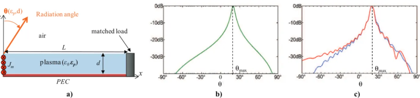
The principle of our antenna is based on the presence of a leaky wave when a source is placed within a plasma layer with a relative permittivity between 0 and 1. The layer is surrounded by air on the top and by a Perfect Electric Conductor (PEC) on the bottom, as shown inFig. 9a. The leaky waves radiate above the layer according to a direction that depends on plasma permittivity, i.e. its electron density. Therefore, it becomes possible to control the beam steering at a fixed frequency via the plasma source. Note that in this case the plasma is not localized as in studies shown in the two previous sections, but directly used as a propagation medium. Therefore, it must not present important electromagnetic losses while having a large size. These constraints are consistent with the willed narrow permittivity range which only requires moderate electron density. Then, it is possible to use low-pressure plasma, which offers both low losses due to the low electron-collision frequency and large volume.
In order to determine the plasma characteristics and better understand the leakage mechanism, we first choose to model a simple 2D configuration composed of a grounded plasma layer of thickness d and of length L as depicted inFig. 9a. The leaky waves are excited in TM mode at 10 GHz by magnetic current line sources Jmoriented along the transverse direction.
In a first approach, we consider an infinite length L. The radiated magnetic field can be calculated with the theoretical analysis used by Tamir et al.[33]. Thus, we can observe the influence of the plasma relative permittivity
ε
pand its thicknessd on the radiation angle
θ
. First, we want to set d before usingε
p as the adjusting parameter to controlθ
. In a simplifiedway, we can say that a minimum value of d is required to excite leaky waves and large values of d allow increasing the scan range mostly in the endfire region. Once the thickness is fixed, varying
ε
p from 0 to 1 leads to small (close to broadside) upto large (close to endfire) radiation angles, respectively. This study allows us to dimension the plasma in a consistent way with the experimental conditions as seen hereafter. Thus, with an electron collision frequency
ν
=
10−8 s−1 which insuressmall losses and with d
=
2 cm, varying the electron density nefrom 1.
24·
1012cm−3 to 4.
7·
1010cm−3leads to a plasmapermittivity range from 0 to 0.9622, which means a radiation angle variation from 1.8° to 79°, as shown inFig. 10a. In
Fig. 9b, we show an example of radiation pattern calculated with ne
=
1.
1·
1012cm−3. In this case, the plasma relativepermittivity is equal to 0
.
11−
j14·
10−4 and the maximum radiation angle denotedθ
maxis 19.6°. It is worth noting that theassumed infinite length of this antenna and the regular exponential decrease along the interface give rise to a radiated field without side lobes. In order to assess the plasma length required and the effects of the antenna truncation, we complete
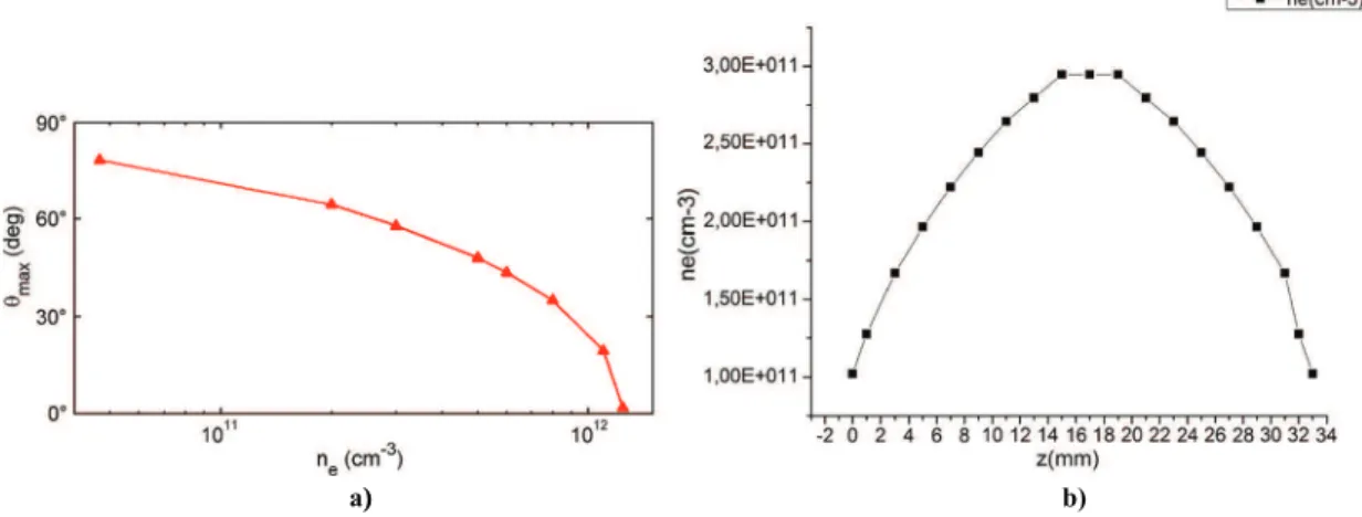
Fig. 10. a) Angle of the maximum radiated fieldθmaxas a function of nefor d=2 cm at 10 GHz / b) Measured electron density profile between two metallic walls placed in a vacuum chamber of inductively coupled reactor in argon at 44·10−3mbar pressure.
Fig. 10. a) Angle du maximum de champ rayonnéθmaxen fonction de nepour d=2 cm à 10 GHz. b) Profil mesuré de la densité électronique entre deux murs métalliques placés dans la chambre à vide d’une source plasma à couplage inductif avec de l’argon à 44·10−3mbar.
our model using Kirchhoff–Huygens integration of the computed field over the plasma/air interface for x between 0 and
L[34]. By this way, we assess the truncation impact and the entire field at L can be considered to be absorbed by a virtual matched load. The far field derived using this method is shown in Fig. 9c for the previous case with L
=
30 cm. We can notice the presence of side lobes below−
10 dB. This result is confirmed by the numerical simulation using Ansys HFSS software[35]. More details about the dimensioning are available in[36].The preliminary design has identified an order of magnitude for the characteristics of the plasma. Thus, the maximum density is about 1012cm−3, with a collision frequency around 108s−1, a thickness of a few centimetres and a maximum
length of 30 cm. These characteristics a priori exclude the DC and AC supplies to create the plasma. Thus, we opted for a RF inductively coupled plasma source which enables us to generate at low pressure a high and stable electron density in a large volume. Besides, in practical cases, the plasma needs to be confined using a second layer at its upper side. We chose the quartz, commonly used by the plasma community, since it meets thermal, mechanical and electromagnetic requirements. Its relative permittivity is 4
.
4−
j4·
10−5 in our operating temperature and frequency ranges[37]. The quartz layer impliestwo main effects. First, it alters the leakage rate due to the variation of its transmission coefficient which depends on
ε
p andθ
. We added this slab in our model with different thicknesses and we observed that leaky waves still exist, withslight angular and directivity shifts. Second, until now, for the sake of simplicity, we assumed a homogeneous plasma layer. Actually, the plasma source and the presence of the PEC and quartz walls give rise to a gradient of electron density. In order to evaluate it, we carried out preliminary measurements of the electron density between two metallic walls placed in a vacuum chamber of inductively coupled reactor available in GREPHE plasma group at the LAPLACE laboratory[38]. An example of measured electron density profile in argon at 44
·
10−3mbar pressure is shown inFig. 10b. The metallic walls,which represent the plasma boundaries along the z direction in our LWA configuration, are separated by d
=
4 cm. We can observe that the electron density is flat in the middle and gradually drops when getting closer to the walls on each side. This case requires a plasma source power of 800 W. It is worth noting that it is not at all dedicated to our application and thus the power required can be drastically reduced with a specific source. Finally, we simulated with the full-wave solver Ansys HFSS a stratified configuration that takes into account the measured electron density profile. We then observed that the gradient does not affect the leaky-wave excitation, but reduces a little the scan range. Further investigations are under way to better quantify this phenomenon.This work constitutes the first step toward the total design and achievement of tunable plasma LWAs. These preliminary results seem to be promising. Our next investigations will deal with the matching of microwave source and the design of specific RF inductively plasma source.
5. Conclusion
In this paper, three examples of the research work made together by a few Toulouse groups are presented at the interface between plasma and microwave physics. These cases illustrate original strategies and results addressing here the use of plasmas for microwave reconfigurability.
The first topic proposes to reverse the usual way that can be found in many microwave papers dealing with plasmas: the devices work well with a specific electron density in a specific volume. The problem is just that they cannot be built. In our method, we first widely characterize what kind of real effect can be achieved before wondering what can be done with it. Hence, a complete experimental setup has been designed and processed as presented in this paper. The results show that
further use of the data can be done focusing on the more interesting behaviours that has been pointed out. Our work is currently done in the context of antennas either looking for losses or phase shift.
The second work presented demonstrates the ability of plasma tubes judiciously localized and operating as switchable defects to control the transmission through an anisotropic EBG structure. Nowadays, this work continues with high power microwave sources.
The third topic addressed in this paper proposes to use large plasma at low pressure to achieve a tunable leaky-wave antenna at a fixed frequency. A specific theoretical model allowed us to validate the concept and to design the plasma. Thus, an inductively coupled plasma source has been chosen to generate a plasma meeting all the requirements. The first results we derived appear promising. Our next investigations will deal with the matching of microwave source and the design of specific RF inductively plasma source.
Beyond the works presented in this paper, the microwave/plasma activities in Toulouse continue and enlarge on issues such as non-linearity control[39]or high-power microwave sources.
Acknowledgements
The authors wish to thank F. Gaboriau and R. Baude, in GREPHE-LAPLACE laboratory, for the helpful measurements performed with their plasma reactor in the framework of our work on leaky-wave antenna and L. Simonchik from Stepanov Institute (Minsk, Belarus) for giving us the plasma tubes shown inFig. 8b.
References
[1]D.E. Anagnostou, A.A. Gheethan, A coplanar reconfigurable folded slot antenna without bias network for WLAN applications, IEEE Antennas Wirel. Propag. Lett. 8 (2009) 1057–1060.
[2]S. Lee, J.-M. Kim, J.-M. Kim, Y.-K. Kim, Y. Kwon, Millimeter-wave MEMS tunable low pass filter with reconfigurable series inductors and capacitive shunt switches, IEEE Microw. Wirel. Compon. Lett. 15 (10) (2005) 691–693.
[3]O.H. Karabey, S. Bildik, S. Strunck, A. Gaebler, R. Jakoby, Continuously polarization reconfigurable antenna element by using liquid crystal based tunable coupled line, Electron. Lett. 48 (3) (2012) 141–143.
[4]T. Zervos, A.A. Alexandridis, F. Lazarakis, M. Pissas, D. Stamopoulos, E.S. Angelopoulos, K. Dangakis, Design of a polarisation reconfigurable patch antenna using ferrimagnetic materials, IET Microw. Antennas Propag. 6 (2) (2012) 158–164.
[5]L.D. Smullin, et al., Microwave Duplexers, Mc Graw-Hill, 1948.
[6]W.M. Manheimer, Plasma reflectors for electronic beam steering in radar systems, IEEE Trans. Plasma Sci. 19 (6) (1991) 1228–1234.
[7]G.G. Borg, et al., Application of plasma columns to radiofrequency antennas, Appl. Phys. Lett. 74 (22) (1999) 3272–3274.
[8]S.E. Lauro, et al., Symmetrical coupled microstrip lines with epsilon negative metamaterial loading, IEEE Trans. Magn. 45 (3) (2009) 1182–1185.
[9]A. Alu, et al., Subwavelength, compact, resonant patch antennas loaded with metamaterials, IEEE Trans. Antennas Propag. 55 (1) (2007) 13–25.
[10]Y.-P. Raizer, Gas Discharge Physics, Springer, 1991.
[11]F. Pizarro, R. Pascaud, O. Pascal, T. Callegari, L. Liard, Experimental study of RF/microplasma interaction using an inverted microstrip line, in: EUCAP 2013, Gothenburg, Sweden, 8–12 April 2013, pp. 8–12.
[12]R.H. Stark, et al., Direct current glow discharges in atmospheric air, IEEE Trans. Plasma Sci. 36 (4) (1999) 3770–3772.
[13]K. Makasheva, et al., Ignition of microcathode sustained discharge, Appl. Phys. Lett. 74 (25) (2008) 1236–1237.
[14]J.-B. Pendry, Negative refraction makes a perfect lens, Phys. Rev. Lett. 85 (18) (2000) 3966–3969.
[15]R.A. Shelby, D.R. Smith, S. Schultz, Experimental verification of a negative index of refraction, Science 292 (5514) (2001) 77–79.
[16]J.-B. Pendry, D. Schurig, D.R. Smith, Controlling electromagnetic fields, Science 312 (5781) (2006) 1780–1782.
[17]E. Yablonovitch, How to be truly photonic, Science 289 (5479) (2000) 557–559.
[18]S. Noda, T. Baba (Eds.), Roadmap on Photonic Crystals, Kluwer Academic, Boston, MA, USA, 2003.
[19]S.N. Burokur, J.-P. Daniel, P. Ratajczak, A. de Lustrac, Tunable bilayered metasurface for frequency reconfigurable directive emissions, Appl. Phys. Lett. 97 (6) (2010) 064101-1–064101-3.
[20]Q. Wang, Y. Zhang, E. Li, S. Yan, B.L. Ooi, Modeling of electromagnetic band gap structure devices tuned by ferrite cylinders, Microw. Opt. Technol. Lett. 43 (5) (2004) 395–400.
[21]T.V. Murzina, F.Y. Sychev, I.A. Kolmychek, O.A. Aktsipetrov, Tunable ferroelectric photonic crystals based on porous silicon templates infiltrated by sodium nitrite, Appl. Phys. Lett. 90 (16) (2007) 161120.
[22]O. Sakai, T. Sakaguchi, K. Tachibana, Verification of a plasma photonic crystal for microwaves of millimeter wavelength range using two-dimensional array of columnar microplasmas, Appl. Phys. Lett. 87 (24) (2005) 241505-1-3.
[23]A. Kallel, J. Sokoloff, T. Callegari, Structure planaire à bande interdite électromagnétique reconfigurable par plasma, in: 12esJournées de caractérisation
microondes et matériaux, JCMM2012, Chambéry, France, 28 March 2012.
[24]S. Varault, B. Gabard, J. Sokoloff, S. Bolioli, Plasma-based localized defect for switchable coupling applications, Appl. Phys. Lett. 98 (13) (2011) 134103-1–3.
[25]J. Lo, J. Sokoloff, T. Callegari, J.-P. Bœuf, Reconfigurable electromagnetic band gap device using plasma as a localized tunable defect, Appl. Phys. Lett. 96 (2010) 251501.
[26]L. Giroud, J. Sokoloff, O. Pigaglio, Reconfigurable Ebg at 18 GHz using perimeter defects, J. Electromagn. Waves Appl. 23 (2009) 1029–1037.
[27]J. Lo, Etude de la reconfigurabilité d’une structure à bande interdite électromagnétique (BIE) métallique par plasmas de décharge, PhD Thesis, Université Paul-Sabatier, Toulouse, 2012.
[28]O. Sakai, K. Tachibana, Plasmas as metamaterials: a review, Plasma Sources Sci. Technol. 21 (2012) 013001-1-18.
[29]S. Lim, C. Caloz, Tatsuo Itoh, Metamaterial-based electronically controlled transmission-line structure as a novel leaky-wave antenna with tunable radiation angle and beamwidth, IEEE Trans. Microw. Theory Tech. 52 (12) (2004) 2678–2690.
[30]A. Alphones, M. Tsutsumi, Leaky wave radiation from a periodically photoexcited semiconductor slab waveguide, IEEE Trans. Microw. Theory Tech. 43 (9) (1995) 2435–2441.
[31]H. Maheri, M. Tsutsumi, N. Kumagai, Experimental studies of magnetically scannable leaky-wave antennas having a corrugated ferrite slab/dielectric layer structure, IEEE Trans. Antennas Propag. 36 (7) (1988) 911–917.
[32]Y. Yashchyshyn, J.W. Modelski, Rigorous analysis and investigations of the scan antennas on a ferroelectric substrate, IEEE Trans. Microw. Theory Tech. 53 (2) (2005) 427–438.
[33]T. Tamir, A.A. Oliner, The spectrum of electromagnetic waves guided by a plasma layer, Proc. IEEE 51 (2) (1963) 317–332.
[34]T. Tamir, A.A. Oliner, The influence of complex waves on the radiation field of a slot-excited plasma layer, IRE Trans. Antennas Propag. 10 (1962) 55–65.
[35] [Online]. Available:http://www.ansoft.com, Ansoft Corporation.
[36]A. Kallel, J. Sokoloff, T. Callegari, Theory and simulations of a beam-scanning plasma antenna, in: 7th European Conference on Antennas and Propaga-tion, EuCAP 2013, Gothenburg, Sweden, 8–12 April 2013, pp. 3457–3461.
[37]J. Krupka, K. Derzakowski, M. Tobar, J. Hartnett, R.G. Geyer, Complex permittivity of some ultralow loss dielectric crystals at cryogenic temperatures, Meas. Sci. Technol. 10 (5) (1999) 387–392.
[38] F. Gaboriau, R. Baude, L. Liard, G. J. M Hagelaar, Experimental characterization of the electron transport across a magnetic field barrier, presented at the 65th Annual GEC, Austin, USA, 22–26 October 2012, Austin, USA.
[39]A. Hamiaz, R. Klein, X. Ferrieres, O. Pascal, J.-P. Bœuf, J.-R. Poirier, Finite volume time domain modelling of microwave breakdown and plasma formation in a metallic aperture, Comput. Phys. Commun. 183 (8) (2013) 1634–1640.