HAL Id: inria-00446054
https://hal.inria.fr/inria-00446054
Submitted on 12 Jan 2010
HAL is a multi-disciplinary open access
archive for the deposit and dissemination of
sci-entific research documents, whether they are
pub-lished or not. The documents may come from
teaching and research institutions in France or
abroad, or from public or private research centers.
L’archive ouverte pluridisciplinaire HAL, est
destinée au dépôt et à la diffusion de documents
scientifiques de niveau recherche, publiés ou non,
émanant des établissements d’enseignement et de
recherche français ou étrangers, des laboratoires
publics ou privés.
Efficient and Flexible Dynamic Reconfiguration for
Multi-Context Architectures
Julien Lallet, Sébastien Pillement, Olivier Sentieys
To cite this version:
Julien Lallet, Sébastien Pillement, Olivier Sentieys. Efficient and Flexible Dynamic Reconfiguration for
Multi-Context Architectures. Journal of Integrated Circuits and Systems, Brazilian Microelectronics
Society, 2009, 4 (1), pp.36-44. �inria-00446054�
1
Efficient and Flexible
Dynamic Reconfiguration for Multi-Context Architectures
Julien LALLET, Sébastien PILLEMENT, Olivier SENTIEYS
INRIA Rennes - Bretagne Atlantique, Université de Rennes, F-22300 Lannion e-mail: [email protected]
ABSTRACT
Dynamic reconfiguration is possible on both fine-grain and coarse-grain architectures. One of the used methodology used consists in the use of multi-context architectures. Unfortunately, the multiple contexts bring power and area overhead. This paper introduces the Dynamic Unifier and reConfigurable blocK (DUCK) concept, a new structure to perform efficiently dynamic reconfiguration on both custom designed fine-grain and coarse grain architectures. The DUCK allows to separate the configuration path and the configuration registers which facilitates simultaneous configuration and computing steps. The reconfiguration process is presented in detail, and synthesis results are given for different structures. Our solution is finally validated with the implementation of a WCDMA (Wideband Code Division
Multiple Access) receiver on a multi-context embedded FPGA and on the dynamically reconfigurable processor DART.
This implementation demonstrates the interest and the efficiency of the use of dynamic reconfiguration and the proposed flexible structure.
Index Terms: Dynamically reconfigurable architectures, Multi-context.
1. INTRODUCTION
Systems on Chip (SOC) are generally based on three main kinds of architecture. First, Application-Specific In-tegrated Circuits (ASIC) allow to efficiently compute an algorithm due to dedicated hardware but are unfortunately inflexible. Secondly, Generic Purpose Processors (GPP) are the most flexible architectures, but compute in an inefficient way. Finally, static reconfigurable architectures such as Field-Programmable Gate Array (FPGA) are considered as a good compromise between processors and ASIC. Meanwhile, mixed architectures have been developed in order to improve the efficiency and the performance of GPP by the use of static reconfigurable co-processors. These static reconfigurable co-processors embedded into an SoC, namely embedded-FPGA (e-FPGA), have allowed GPP to follow application developments. Dynamic reconfiguration allows partial configurations at run-time, and thus improves performances. Some specific processors and FPGAs take advantage of dynamic reconfiguration in their architecture by the use of the multi-context process. This architectures are either Dynamically Reconfigurable Processors (DRP) or Dynamically Reconfigurable FPGAs. This is achieved by the local storage of any possible context. When a new configuration is required, the system switches between one or the other context. The major drawback of this solution is the silicon area and power inefficiency caused by local memories needed to store all the contexts. Our contribution to multi-context DRA is the definition of a flexible and optimized structure that supports dynamic, partial and run-time reconfiguration dedicated to both fine-grain and coarse-fine-grain DRA structures. This is performed by only two configuration memories, one current config-uration memory and one parallel configconfig-uration memory. The parallel configuration memory is used for loading or saving contexts for preemption to or from the configuration
memory in one clock cycle. New contexts are stored in this parallel configuration memory thanks to a splittable scan-chain. Compared to previous multi-context Dynamically Reconfigurable Architectures (DRA), configurations exploit efficiently the available silicon resources and enables the implementation of any kind of computing granularity.
The paper is structured as follows. Section 2 describes related works on optimization of multi-context DRA. Sec-tion 3 presents our contribuSec-tion on dynamic reconfiguraSec-tion processes of DRA. In Section 4, we present the experi-mental method and discuss results on a WCDMA receiver implementation on an e-FPGA and on the dynamically reconfigurable processor DART. Finally, Section 5 sums up this paper.
2. RELATEDWORKS
For a decade, many dynamically reconfigurable architec-tures have been developed but only a few can be considered as multi-context architectures, as they locally store one or more parallel contexts. NEC-DRP [7] is a massively parallel processor architecture. Reconfiguration processes are managed by a central manager which can select one futur context from 16 multi-context memories. For the archi-tecture XPP [13] (eXtreme Processing Platform), dynamic reconfiguration is managed by a hierarchical manager com-posed of a tree of sub-managers. A cache memory placed in parallel of the configuration memory enables multi-context reconfiguration. The Adres architecture [14] (Architecture
for Dynamically Reconfigurable Embedded Systems) stores
its configuration either in a RAM configuration memory or in the hierarchical memories for bigger configuration spaces. The main constraint of these architectures comes on one hand from the few flexibility offered by these architectures in terms of computing granularity, and, on the other hand, from the fact that this architectures do not
to achieve an efficient reconfiguration from their parallel memory.
The only fine-grain architectures which implement dy-namically reconfigurable computing are multi-context FP-GAs. Commercial FPGAs (e.g. Xilinx Virtex family) allow dynamic reconfiguration, but the reconfigured resources have to be stopped before a new configuration can be prop-agated [2]. Different approaches have been proposed in the literature to reduce the excessive silicon area used by multi-context FPGAs. First, some works focus on the reduction of the configuration words. In [6], the method consists in the limitation of the connection map inside a switch box. In [1], the authors reduce the context memory by using redundancy and regularity in the configuration data. The first method has the disadvantage to reduce routability. The second is efficient only in good conditions of redundancy and regularity, which is not the case for all applications. The second approach [3] is a technological solution which consists in the use of DRAM memories instead of SRAM usually implemented for storing configuration contexts. This allows to save between 10% and 60% transistors, but causes a new problem concerning mixed process of DRAM and logic.
3. EFFICIENTDYNAMICRECONFIGURATION
In this section, we present the resource that is proposed to make the reconfiguration efficient and flexible, whatever to the granularity of the computing resource.
A. DUCK: Dynamic Unifier and reConfiguration blocK
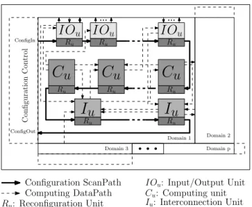
As mentioned in Section 2, multi-context reconfiguration has provided solutions for fast reconfiguration but generates redundant resources (local context memories) which con-tributes to a power inefficient design even if some solutions have been developed. However, the solution that we propose in this paper needs only one context memory for each resource, independently of the granularity of the computing resource. But, using only one context memory means that it is necessary to develop other architectural concepts in order to maintain the timing constraints and the flexibility required by today’s applications. The first concept of our contribution consists in the isolation of the configuration paths and the configuration resources which allows to prepare new contexts during the computation. The Dynamic Unifier and reConfiguration blocK (DUCK) is in charge of the configuration path and has to swap the required contexts to the configuration registers when needed. The second concept consists in the possibility to split the configuration path while maintaining a unique computing path in order to propagate the configuration through several configuration paths at the same time. Each configuration path composes a reconfiguration domain. Figure1 shows an example of the implementation of the DUCK concept. This basic exam-ple imexam-plements interconnection units (Iu), computing units
(Cu), input and ouput units (IOu) and reconfiguration units
(Ru) namely the DUCK resources. For each units (Iu, Cu
or IOu) one DUCK (Ru) is associated and composes the
configuration path (black arrow in bold print). The inputs of the two configurations paths are represented by the name
I Ou: Input/Output Unit Cu: Computing unit Iu: Interconnection Unit Ru: Reconfiguration Unit Domain 1 Domain 2 Domain p Domain 3
I O
uI
u
I
u
C
u
Configuration Con trol RuI O
uI O
u Ru Ru Ru Ru Ru Ru RuC
u
C
u
Computing DataPath Configuration ScanPath ConfigIn ConfigOutFigure 1. Example of a DRA composed of several kind of
resources
Conf igIn(i) and the outputs by the name Conf igOut(i). When the system is ready to reconfigure, each DUCK swaps the configuration context from its internal registers to the control registers of each unit. Once the configuration is swapped, it is possible to extract the context through the configuration path.
B. Dynamically Reconfigurable Architectures
According to the resource to reconfigure, the DUCK implement different functions. In our DRA model, the communication resources, called DyRIBox (Dynamically Reconfigurable Interconnection Box), switch signals from input ports to output ports. Each DyRIBox has niinputs and
mioutputs on b bits at each i of its four sides (North, South,
West, East). The total number of input and output ports is
therefore N = !3
i=0ni and M =!
3
i=0mi respectively.
Depending on the value of the configuration register, each input can be connected to one or several outputs. To reduce the complexity and the size of the configuration stream of the DyRIBox, the number of inputs that can be switched to an output is set to P , with P ≤ N . Therefore, the DyRIBox contains M configuration registers of "p = log2P # bits.
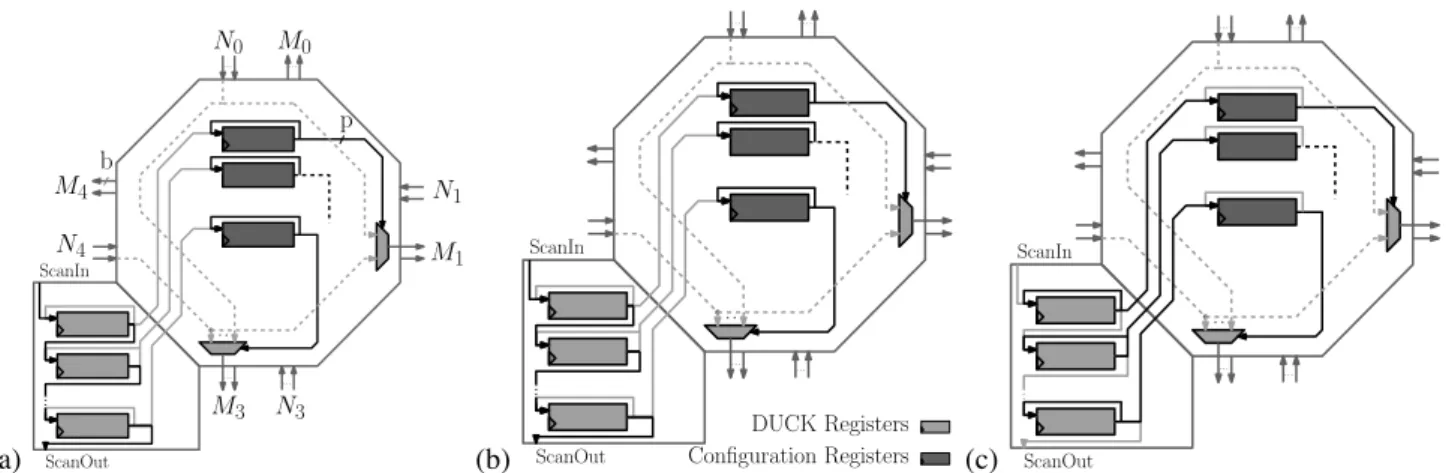
In case of classical dynamic reconfiguration, the recon-figuration time is too long for the given timing constraints. To reduce this time, the reconfiguration process of the DyRI-Box and of the computing resources is based on DUCK context registers (Figure2). Each configuration register is connected to one context register contained in the DUCK resource and data could be swapped when needed.
In order to manage the reconfiguration process, all DUCK registers are interconnected through a scanpath bus. Scanpath registers are used in design-for-test (DFT) techniques instead of classical registers in order to extract the register value at any time. The scanpath bus creates a unique big shift register with all the scanpath registers of the architecture. Thus, the extracted data flow is compared with the test vectors during testing to detect errors in the computing path. This method has been cited in [4] for applying preemption in reconfigurable architectures but has
(a) ScanIn ScanOut ... ... ... ... ... N0 M0 N1 M1 N3 M3 M4 N4 b p (b) ScanIn ScanOut ... ... ... ... ... Configuration Registers DUCK Registers (c) ScanIn ScanOut ... ... ... ... ...
Figure 2. Reconfiguration process inside the DUCK structure
not yet been implemented. This was due to the fact that the extraction time was too long for the given timing constraints required by today’s applications.
The use of the configuration path in a scanpath manner associated with the DUCK concept allows the system to be reconfigured in one clock cycle. The use of the DUCK registers allows the system to prepare the next configuration while it is computing. The propagation of a new context is done by three different steps. First, the configuration regis-ters are already loaded with the current context (Figure2(a)). The DUCK registers are waiting for the next step. Either the new configuration is already propagated, or is waiting to be configured. The second step (Figure2(b)) shows how a new configuration is spread to the DUCK registers. As explained before, the DUCK is connected in a scanpath manner which allows to propagate the next context. In case of preemption, the process is still the same for extraction of the previous context. Finally, each DUCK register swaps its data with the configuration register. Every configuration register is directly connected to a DUCK register. It is noteworthy that in case of a new configuration identical to the current one, the configuration swap does not disrupt the interconnection and computing resource behavior. Therefore, reconfigura-tion is possible even if a computing datapath crosses a reconfiguration area which it does not belong to.
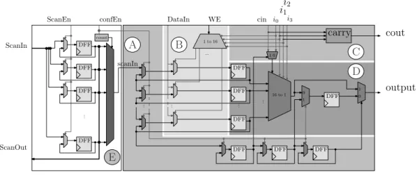
Today’s SOCs use very different kinds of computing resources, so that, for every new dynamically reconfig-urable architecture or computing resources, it becomes more difficult to extract an homogeneous reconfiguration protocol. The DUCK aims to solve this issue. For example, considering a classical logic cell (gray area on Figure3) several resources are part of it. The reconfiguration path (area$) allows to set or reset the output register, to selectA
the sequential or combinatorial output, and to select the carry input. The memory area ($) allows to use the logicB
cell as a RAM memory. The carry resources are needed for arithmetic operations (area$). The LUT resources areC
needed for the implementation of logical functions (area
D
$).
The configuration path goes through all configuration registers and LUT registers. In this example, one logic cell needs 20 clock cycles to be reconfigured. Thus, for an e-FPGA composed of a n·m array of logic cells, n·m·20 clock cycles are needed to reconfigure the whole FPGA. This time
is not acceptable for fast reconfiguration. Our solution, the DUCK (area$ of Figure3) allows to shift the configurationE
context locally in the same way as for the DyRIBox and to swap the reconfiguration when needed. Therefore, the whole embedded FPGA can be reconfigured in 20 clock cycles. In the DUCK, a counter selects each configuration register one after the other and shifts it to the logic cell configuration path.
C. Results and Exploration
We present here exploration results on the DUCK pa-rameters. First, synthesis results are given to estimate the impact on silicon area of the size of outputs and inputs, and the number of possible connections to one output. The critical path and power consumption are also analyzed. All results are expressed as a function of the computing data bitwidth. Results are obtained with the synthesis tool Design Compiler from Synopsys and for a 130nm CMOS technology.
The influence of DUCK parameters on design area, power and critical path is given in Figure4. The results have been obtained by changing the number of outputs on the DyRIBox. First, the DUCK has clearly no influence on the critical path results because of the physical separation of the configuration path and the configuration registers in the DyRIBox. Secondly, the more connection possibility the DyRIBox has, the less impact the DUCK has in the design area. This is explained by the fact that the silicon area used for the interconnection wires between inputs and outputs grows faster than the silicon area used by the configuration/DUCK memories. Due to custom libraries used for 8-bit words, the power consumption is better controlled from this bitwidth than for 4-bit data.
The interconnection network presented in [9] consists in a set of reconfigurable circuit-switched routers intercon-nected by links. One router is composed of five 16-bit bi-directional ports connected through a 16x20 fully connected crossbar. We have generated and synthesized a DyRIBox associated to a DUCK with the same functionality. The results are given for the 130 nm CMOS technology from ST Microelectronics. Area, frequency and power after synthesis are given for the two solutions in Tab.I. These results show that the simplicity of our solution allows to keep as many flexibility as in their solution, whereas our structure has only
... count ScanIn scanIn output cin i0 i1 i2 i3 confEn 1 0 0 1 16 to 1 1 to 16 ... ... ... ... ... 0 1 C D A B E ScanEn ScanOut DataIn WE carry cout DFF DFF DFF DFF DFF DFF DFF DFF DFF DFF DFF
Logic Bloc : 20 configuration bits DUCK
Figure 3. Simple logic cell architecture developed for fast reconfiguration
0 10 101 102 1.2 1.3 1.4 1.5 1.6 1.7 1.8 1.9 2.0 2.1 Number of outputs Duck Overhead Area Power
Figure 4. Influence of DUCK on area, power and time
4% area overhead and a gain of 25% on the critical path and of 69% in power.
In conclusion, fast dynamic reconfiguration is made possible by the use of the DUCK concept: the separation of configuration path and the configuration registers. A small overhead of silicon area for each logic cell and interconnect box is involved by our method, but on the other hand, the reconfiguration itself allows to save resources compared to multi-context DRAs. Furthermore, to maintain the timing constraint, it is necessary to propagate each new context as fast as possible, so that the new tasks can swap in the most efficient way. That is realized by the introduction of the split configuration path. Indeed, when several configuration paths are created, it is possible to propagate new contexts in parallel with each configuration path. This method allows to reduce the propagation time with regard to the number of configuration path used. The
Table I. Synthesis results compared with the 4S project solution
Interconnection Area Critical Power in mm2 Path in ns in mW 4S project 0.0506 930 17.32
DyRIBox 0.0526 692 7.22
following case study gives more precise results about saved resources on a telecommunication application.
4. CASE-STUDY
In this section, we present the implementation of a
Wideband Code Division Multiple Access WCDMA receiver
on our embedded FPGA (Figure6) and on the dynamically reconfigurable processor DART. WCDMA is a high-speed transmission protocol used in third generation mobile com-munication systems such as UMTS (Universal Mobile Tele-communications System), and is considered as one of the most critical applications of third-generation telecommuni-cation systems. It is based on the CDMA access technique where all data sent within a channel and for a user to have to be coded with a specific code to be distinguished from the data transmitted in other channels [8]. The number of codes is limited and depends on the total capacity of the cell, which is the area covered by a single base station. To be compliant with the UMTS radio interface specification (UTRA – Universal Terrestrial Radio Access), each channel must achieve a data rate of at least 128kbps. The theoretical total number of concurrent channels is 128 channels. As in practice only about 60% of the channels are used for user data, the WCDMA base-station can support 76 users per carrier.
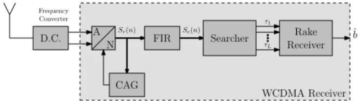
The WCDMA application executed on our reconfigurable architecture consists in the alternate execution of three main tasks (Figure5): FIR (Finite Impulse Response) filter,
Searcher, and Rake Receiver. Within a WCDMA receiver,
real and imaginary parts of the signal received on the an-tenna after demodulation and digital-to-analog conversion, Sr(n), are filtered by an FIR (Finite Impulse Response)
shaping filters. Since the transmitted signal reflects in
obstacles like buildings or trees, the receiver gets several replicas of the same signal with different delays and phases. By combining the different paths, the decision quality is drastically improved. Consequently, the Rake Receiver combines the different paths extracted by the Searcher block in order to improve the quality of the symbol decision. Each path is computed by one finger which correlates the received signal by a spreading code aligned with the delay of the
N A D.C. Rake ˆb Receiver Frequency Converter Sr(n) Se(n) CAG FIR Searcher τ1 τL WCDMA Receiver
Figure 5. WCDMA receiver synoptic
multipath signal. In our case, a maximum number of fingers are considered. This task is realized at the chip rate of 3.84 MHz. The decision is finally done on the combination of all these spreaded paths.
A. Timing Constraints
WCDMA is the highest speed transmission protocol used in the UMTS system. The bandwidth of the transmitted signal is equal to 5 MHz. The frequency of the code corresponding to the chip rate (Fchip) is fixed to 3.84 MHz.
One slot is composed of 256 chip data. Registers are used to pipeline data while FIR, Searcher or Rake Receiver are computing in one slot. For better synchronization results, the received chip is 4-time over-sampled. The computing time available for the three functions (FIR, Searcher, and
Rake Receiver) is therefore tslot = 66.6µs between the
computation of two consecutive slots. The FIR and Searcher computes on 1024 samples while one Finger of the Rake
Receiver computes on 256 samples. One sample is
com-puted at each clock cycle.
B. e-FPGA implementation
The implementation of the WCDMA receiver on an hardware accelerator composed from standard logic cells as such implemented in a FPGA architecture is presented. The interaction of a DUCK and a logic cells allows the architecture to reconfigure the whole resources in parallel.
Table II presents synthesis results obtained with the VPR [15] and ABC Berkeley [16] frameworks. The most complex function, the searcher, requires 4953 logic cells to be configured in the e-FPGA. It is therefore possible to implement the whole WCDMA decoder into 4953 logic cells using dynamic reconfiguration. To illustrate dynamic reconfiguration, the three functions are executed sequen-tially in a time slot of 66.6µs i.e. 22.2µs for each function. Therefore, each function is executed during 22.2µs while the next context is propagated. As said previously, each function is completed in 1024 clock cycles, and the clock frequency is therefore greater than 46.55 MHz. The logic cell critical path has a value of 0.6ns in a 130nm CMOS technology. Considering that the functions have a critical path of 13 logic cells, the computing frequency can be up to 128.2 MHz. For a better power consumption, the frequency can be reduced to a lower value maintaining the timing constraint. For this implementation, the computing frequency is set to 50 MHz (tcomputing = 20.48µs).
To perform dynamic reconfiguration, 4953 logic cells need to be reconfigured in less than 22.2µs. One logic cell has 20 reconfiguration bits and a DyRIBox 10 bits. A 6-bit width configuration path is used for its good
trade-off between performance and silicon area. Therefore, 4953 × 30/6 = 24765 6-bit words are needed for each context.
Thanks to our system architecture, the global config-uration is split into 8 reconfigconfig-uration domains managed in parallel. Using a 300M Hz clock frequency for the reconfiguration process allows to reconfigure in less than 11µs.
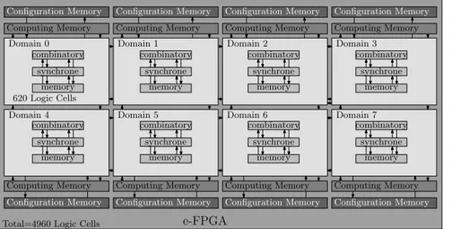
Figure 6 shows the implemented architecture with 8 domains of 620 logic cells. Static memory is used to allow data exchange between each functions. Light-gray areas represent the 8 configuration paths composed of 620 logic cells each. Each WCDMA function can be implemented on this architecture. The FIR function is depicted as task T1. Its implementation requires all domains and thus designs a unique computing path. The Searcher function requires also the 8 domains and thus designs also a unique computing path. The last function, Rake Receiver, can be split on 8 computing paths. One computing path for one finger. Assuming that a Finger implementation requires 561 logic cells, one domain is used for each finger. The 59 remaining logic cells are used to realize the decision on symbol.
Figure 7 shows that the process of propagation, comput-ing and reconfiguration is fast enough to maintain the timcomput-ing constraints thanks to the DUCK resources in the DyRIBox and the logic cell. On one slot time, the DUCK resources are able to extract the previous context or propagate the future context. P reeRF S means preemption of the Rake receiver
or FIR or Searcher contexts and ConfRF S means
configu-ration of the Rake receiver or FIR or Searcher contexts. The
NOP operation means that the DUCK resources are waiting
for working. Domain 0 and Domain 1 are giving an example of a complete WCDMA computing implementation includ-ing Finclud-inger implementation. Domain 7 gives an example where no Finger needs to be implemented. The computing time (tcomputing) represents the available computing time of
one function, the propagation time (tpropagation) represents
the available time for the configuration and the preemption processes, and the reconfiguration time (tr) represents the
time needed to reconfiguration the whole domain. The synthesis results the silicon overhead of the added local configuration memories. The overhead silicon area of the
DUCK resource is 998µm2
for a DyRIBox and 1468µm2
for a logic cell. Considering that 4960 of the two resources are implemented, the overall area overhead can be estimated at 12.23mm2
. It is important to notice that 12926 logic cells should have been used for a static implementation. Our im-plementation using dynamic reconfiguration consumes 7966 logic cells less than the static implementation. Considering that the silicon area needed for a logic cell is 2160µm2
and 6850µm2
for a DyRIBox, we can estimate the saved area to 59mm2
. Thanks to partial reconfiguration offered by today’s Xilinx FPGAs, it could be possible to implement a
Table II. Necessary logic-cells for WCDMA decoder
implemen-tation on a dynamically reconfigurable architecture
FIR Searcher a FingerRake ReceiverAll Logic cells 3475 4953 561 4488
e-FPGA
Domain 0 Domain 1
Domain 4 Domain 5
Total=4960 Logic Cells
Static resources
Dynamically reconfigurable resources Domain 2 Domain 3 Domain 6 Domain 7 combinatory synchrone memory combinatory synchrone memory combinatory synchrone memory combinatory synchrone memory combinatory synchrone memory combinatory synchrone memory combinatory synchrone memory combinatory synchrone memory
e-FPGA configuration for FIR execution T 1
e-FPGA configuration for Searcher execution T 2
T 3aT 3bT 3cT 3d T 3eT 3fT 3gT 3h
e-FPGA configuration for Rake Receiver execution 620 Logic Cells
Computing Memory
Configuration Memory Configuration Memory Configuration Memory Configuration Memory
Configuration Memory Configuration Memory Configuration Memory
Configuration Memory
Computing Memory Computing Memory
Computing Memory Computing Memory Computing Memory
Computing Memory Computing Memory
Figure 6. Resource allocation of the implemented embedded FPGA
WCDMA decoder on two areas of 4960 logic cells. This solution requires 4960 logic cells more than our dynamic implementation.
Finally, Table III compares the same WCDMA decoder implemented in a Xilinx Virtex FPGA. It can be easily concluded that a dynamic reconfiguration is not possible on the Virtex since the reconfiguration of the entire FPGA takes more than 2ms [12] with a configuration frequency of 60M Hz and with the SelectMAP interface which enable 8-bit word configuration.
C. DART implementation
In this section, we present the implementation of the WCDMA receiver on a hardware accelerator composed from the computing resources of the DART architecture.
The dynamically reconfigurable processor DART [11] is a coarse-grain reconfigurable architecture developed mainly for 3G mobile telecommunication application do-main. DART architecture is build around six computing elements called DPR (DataPath Reconfigurable Figure 8). Each DPR is composed of two registers (reg), four Address Generators (AG) to access four local memories (Datamem), and four FUs (functional units two adder/subtracters and two multipliers). The DPR is fully configurable thanks to a fully connected multi-bus. The original architecture was fixed and it was not possible to modify the structure of the DPR.
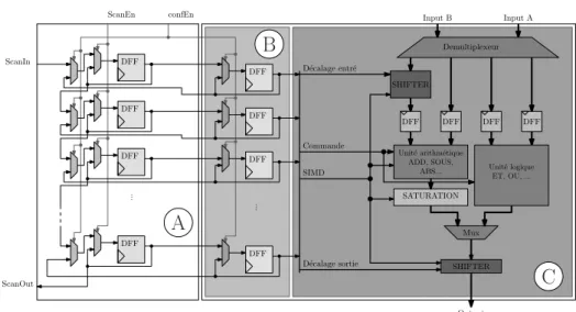
A DPR reconfiguration is executed in either 3 or 9 clock cycles.Thanks to the DUCK concept and the parallelization of the reconfiguration processes, this reconfiguration is reduced to one clock cycle. An example of the interaction between a functional unit of a DPR and its dedicated DUCK is given Figure 9. In this example, each bit register used for the configuration of the functionnality of the FU becomes
Table III. Comparison between results on an embedded FPGA
solution and on a Virtex commercial FPGA
System LogicCells Size (8-bit word)Configuration ReconfigurationTime e-FPGA 4960 36k 22.2µs XCV200 5292 164k 2.53ms
Nested loop support
AG1 AG4 Data mem1 Multi-bus network FU1 FU4
DPR
To segmented network AG2
Data mem2 FU2 Data mem4 AG3 Data mem3 FU3 reg1 reg2
Figure 8. A DPR computing element of the DART reconfigurable
architecture
Table IV. Configuration size for each unit of one cluster of six
DPR
RECONFIGURATION SIZE(BITS) SIZE(BITS) SIZE(BITS)
TARGET /RESOURCE /DPR /CLUSTER
AG 1 4 24
Registers 1 6 36
Add/Subb(FU1-3) 3 6 36
Multiplier(FU2-4) 11 22 132
TOTAL 38 228
a parallel configuration register so that each configuration bit can be switched. Each DPR requires Nbconf P E = 38
configuration bits (Tab.IV). Figure 10 shows the imple-mented architecture with 6 DPR needed for this application. Therefore, 228 bits are needed for each configuration of the whole DART architecture, interconnection DUCK excepted. Two kinds of interconnection units are used. First, one
DPR1
Cluster
Data. Mem. DPR2 DPR3 DPR4 DPR5 DPR6 Ctrl. DMA Ctrl. Config. Mem. R ´eseau Segmen t´eCœur de traitement d´edi´e
Domain 0 Domain 7 Time tslot tcomputing tr tpropagation Computing Path Configuration Path Searcher NOP ConfF FIR Searcher Finger 0 FIR r r r r r
NOP NOP NOP
NOP P reeF ConfR
P reeF ConfR
ConfS
P reeR NOP NOP
NOP P reeS ConfF Domain 1 Searcher Finger 1 FIR r r r NOP P reeF ConfR ConfS
P reeR NOP NOP
NOP P reeS ConfF
Figure 7. Gantt diagram of computing and reconfiguration process
... ScanIn ScanOut ScanEn confEn DFF DFF DFF DFF ... DFF DFF DFF DFF
C
B
A
Output Input B Input A DFF DFF DFF DFF Demultiplexeur SHIFTER SATURATION MuxUnit´e arithm´etique ADD, SOUS,
ABS... Unit´e logique ET, OU, ... SHIFTER D´ecalage entr´e Commande SIMD D´ecalage sortie
Figure 9. DUCK generated for a fast reconfiguration on DART architecture
kind of interconnection (DBdpr) is necessary to connect all
the resources inside a DPR. 18 inputs are connectable to 10 outputs. Therefore, the configuration size (T CDBdpr)
of this interconnection unit requires :
T CDBdpr= 10 × "log2(18)# = 50 bits (1)
The second kind of interconnection unit (DBcluster)
is an 8-bitwidth crossbar type and is necessary for the communication between the 60 registers and functional units of all the DPR inside one cluster with a maximum of 30 possible connections. Therefore, the configuration size (T CDBcluster) of this interconnection unit requires :
T CDBcluster = 8 × "log2(30)# = 40 bits (2)
The WCDMA implementation on DART has already been presented in [10]. The configuration size of all inter-connection units (T CDB) requires T CDB = 6×50+40 = 340 bits. The complete bitstream size for the whole DART architecture (T CDART) requires T CDART = 228 + 340 =
568 bits. On DART, the reconfiguration is executed at the same frequency as the processing frequency, which is up to 130 MHz for the reference design in [11].
The number of domains needed (ND) is specified by the
available time between two configurations (P ropt). P ropt
is determined by the number of registers to reconfigure and
the speed of the configuration memory to read the bitstream which is equal to 300 MHz. A complete new context can be propagated in
P ropt=
580/8
300E6 = 240 ns (3)
The shortest propagation time available is executed dur-ing the channel estimation function. This context is only implemented during 8 clock cycles. Considering that for this application, the working frequency is fixed to 93 MHz, the propagation time available is then equal to 86.22 ns. Therefore, the number of reconfiguration domain required to maintain the reconfiguration constraints are equal to:
ND=
" 241E−9
86.22E−9
#
= 3 (4)
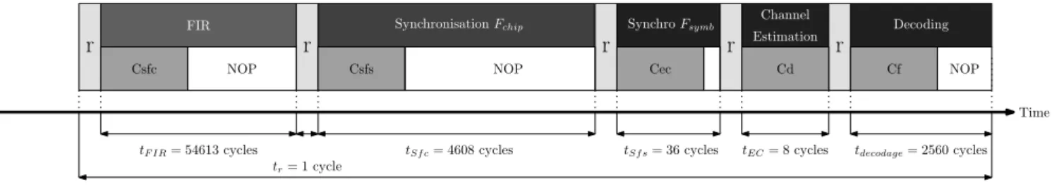
Figure 11 shows the timing implementation of the differ-ent functions on one reconfiguration domain. Each domain receives the same configuration in parallel. While the cluster computes, the DUCKs are receiving the different config-uration simultaneously. Next configconfig-urations are prepared during the execution of the functions. Csf c stands for configuration of the function Synchronisation Fchip, Csf s
for configuration of the function Synchronisation Fsymb,
Cec for configuration of the function Channel Estimation, Cd for configuration of the function Decoding, and Cf for configuration of the function FIR.
Time
tslot
tF IR= 54613 cycles
Synchronisation Fchip
FIR Synchro Fsymb
r
r
r
r
r
tr= 1 cycle
tSf c= 4608 cycles tSf s= 36 cycles tEC= 8 cycles tdecodage= 2560 cycles
NOP NOP NOP
Csfc Csfs Cec Cd Cf
Estimation Channel
Decoding
Figure 11. Gantt diagram of computing and reconfiguration process for the DART implementation
5. CONCLUSIONS
In this paper, a new fast dynamically reconfigurable concept for embedded hardware accelerator is proposed. This method allows to use dynamic reconfiguration and to gain in flexibility and in silicon area while maintaining the timing constraints. The reconfiguration time is reduced compared to traditional FPGA or DRP. The proposed con-cept is based on the isolation of the configuration paths and the configuration resources, which allows to prepare new contexts during the computations. The second concept consists in the possibility to split the configuration path while maintaining a unique computing path in order to propagate the configuration through several configuration paths at the same time. In the near future, we will develop exploration tools in order to estimate the possible configu-ration paths to automatically get the best trade-off between speed, performance and silicon area.
ACKNOWLEDGMENTS
This work has been performed in the context of the CoMap project and is financed by the French Ministry of Foreign Affairs. The authors would like to thank A.Kupriyanov, D.Kiessler, F.Hanning, J.Teich, B.Pottier and R.Keryell for their fruitfull collaboration.
REFERENCES
[1] M. Hariyama, W. Chong, S. Ogata, and M. Kameyama. Novel Switch Block Architecture Using Non-Volatile Functional Pass-Gate for Multi-Context FPGAs. In Proceedings of the IEEE Computer Society Annual Symposium On VLSI (ISVLSI),2005, pages 46–50. [2] I. Robertson and J. Irvine. A Design Flow for Partially
Recon-figurable Hardware. ACM Transaction on Embedded Computing Systems, vol. 3, no. 2, May 2004, pages 257–283.
[3] D. Kawakami, Y. Shibata, and H. Amano. A prototype chip of multicontext FPGA with DRAM for Virtual Hardware. In Asia and South Pacific Design Automation Conference (ASP-DAC), 2001, pages 17–18.
[4] D. Koch, A. Ahmadinia, C. Bobda, H. Kalte, and J. Teich. FPGA Architecture Extensions for Preemptive Multitasking and Hardware Defragmentation. In Proceedings of the IEEE Conference on Field-Programmable Technology (FPT), 2004, pages 433–436.
[5] L. Lagadec and B. Pottier. Object-Oriented Meta Tools for Recon-figurable Architectures. In Proceedings of the SPIE Conference on Modeling, Signal Processing, and Control , 2000, pages 69–79. [6] V. B. Lecuyer, M. A. Aguirre, A. B. Torralba, L. G. Franquelo, and J.
Faura. Decoder-Driven Switching Matrices in Multicontext FPGAs: Area Reduction and Their Effect on Routability. In Proceedings of the IEEE International Symposium on Circuits and Systems (ISCAS), 1999, pages 463–466.
[7] M. Suzuki, Y. Hasegawa, V. M. Tuan, S. Abe, and H. Amano. A Cost-Effective Context Memory Structure for Dynamically Reconfigurable Processors. In Proceedings of the IEEE International Parallel and Distributed Processing Symposium (IPDPS), 2006, pages 1101–1109. [8] T. Ojanpera and R. Prasad. Wideband CDMA For Third Generation Mobile Communication. Artech House Publishers, Norwood, MA, USA, 1998.
[9] P. T. Wolkotte, G. J. M. Smit, and J. E. Becker. Energy-Efficient NoC for Best-Effort Communication. In Proceedings of the Inter-national Conference on Field-Programmable Logic, Reconfigurable Computing, and Applications (FPL), 2005, pages 197–202. [10] R. David, D. Chillet, S. Pillement, and O. Sentieys. DART: A
Dynamically Reconfigurable Architecture Dealing with Future Mo-bile Telecommunications Constraints. In Proceedings of the IEEE Reconfigurable Architectures Workshop (RAW), 2002, pages 118– 123.
[11] S. Pillement, R. David, and O. Sentieys. DART : A Functional-Level Reconfigurable Architecture for High Energy Efficiency. In EURASIP Journal on Embedded Systems, vol. 2008, January 2008, 13 pages.
[12] Xilinx. Virtex series configuration architecture. Technical report, 2004.
[13] V. Baumgarte, G. Ehlers, F. May, A. Nückel, M. Vorbach and M. Weinhardt PACT XPP - A Self-Reconfigurable Data Processing Architecture, Journal of Supercomput, 2003, pages 167–184. [14] B. Mei, A. Lambrechts, D. Verkest, J. Y. Mignolet and R. Lauwereins.
Architecture Exploration for a Reconfigurable Architecture Template, in IEEE Journal of Design and Test, March 2005, vol. 22, no. 2, pages 90–101.
[15] V. Betz and J. Rose. VPR: A new packing, placement and routing tool for FPGA research. in Proceedings of the International Conference on Field-Programmable Logic and Applications (FPL), 1997, pages 213–222.
[16] J. Pistorius, M. Hutton, A. Mishchenko, and R. Brayton. Bench-marking Method and Designs Targeting Logic Synthesis for FPGAs. In Proceedings of the ACM/SIGDA International Workshop on Logic and Synthesis (IWLS), 2007, pages 230–237.