HAL Id: hal-02327808
https://hal.archives-ouvertes.fr/hal-02327808
Submitted on 29 Dec 2020HAL is a multi-disciplinary open access archive for the deposit and dissemination of sci-entific research documents, whether they are pub-lished or not. The documents may come from teaching and research institutions in France or abroad, or from public or private research centers.
L’archive ouverte pluridisciplinaire HAL, est destinée au dépôt et à la diffusion de documents scientifiques de niveau recherche, publiés ou non, émanant des établissements d’enseignement et de recherche français ou étrangers, des laboratoires publics ou privés.
Reflective Back Contacts for Ultrathin
Cu(In,Ga)Se2-Based Solar Cells
Louis Gouillart, Wei-Chao Chen, Andrea Cattoni, Julie Goffard, Lars Riekehr,
Jan Keller, Marie Jubault, Negar Naghavi, Marika Edoff, Stéphane Collin
To cite this version:
Louis Gouillart, Wei-Chao Chen, Andrea Cattoni, Julie Goffard, Lars Riekehr, et al.. Reflective Back Contacts for Ultrathin Cu(In,Ga)Se2-Based Solar Cells. IEEE Journal of Photovoltaics, IEEE, 2019, 10 (1), pp.250-254. �10.1109/JPHOTOV.2019.2945196�. �hal-02327808�
Reflective back contacts for ultrathin Cu(In,Ga)Se
2-based solar cells
Louis Gouillart
1,2, Wei-Chao Chen
3, Andrea Cattoni
1, Julie Goffard
1, Lars Riekehr
3, Jan Keller
3, Marie
Jubault
4, Negar Naghavi
2, Marika Edoff
3, Stéphane Collin
11
Centre for Nanoscience and Nanotechnology (C2N), CNRS, Univ. Paris-Sud, Université Paris-Saclay,
91120 Palaiseau, France;
2CNRS, UMR 9006, IPVF, 30 Route Départementale 128, 91120 Palaiseau,
France;
3Ångström Solar Centre, Division of Solid State Electronics, Uppsala University, PO Box 534,
SE-75121 Uppsala, Sweden;
4EDF R&D, IPVF, 30 Route Départementale 128, 91120 Palaiseau, France
Abstract — We report on the development of highly reflectiveback contacts made of multi-layer stacks for ultrathin CIGS solar cells. Two architectures are compared: they are made of a silver mirror coated either with a single layer of In2O3:Sn (ITO)
or with a bilayer of ZnO:Al/ITO. Due to the improvement of CIGS rear reflectance, both back contacts result in a significant EQE enhancement, in agreement with optical simulations. However, solar cells fabricated with Ag/ITO back contacts exhibit a strong shunting behavior. The key role of the ZnO:Al layer to control the morphology of the top ITO layer and to avoid silver diffusion through the back contact is highlighted. For a 500 nm-thick CIGS layer, this optimized reflective back contact leads to a best cell with a short-circuit current of 27.8 mA/cm² (+2.2 mA/cm² as compared to a Mo back contact) and a 12.2%-efficiency (+2.5% absolute).
Index Terms — photovoltaic cells, ultrathin Cu(In,Ga)Se2,
reflective back contacts, In2O3:Sn.
I. INTRODUCTION
Developing ultrathin Cu(In,Ga)Se2 (CIGS) solar cells, i.e.
with an absorber thickness of 500 nm or less, is a promising way to improve the competitiveness of CIGS by reducing its manufacturing cost [1]–[3]. However, the efficiencies of ultrathin solar cell suffer from low short-circuit currents (JSC)
due to insufficient light absorption in ultrathin CIGS layers and high recombination velocities at CIGS back interface with Mo [4], [5]. While the rear passivation of ultrathin CIGS layers was shown to improve JSC thanks to a better carrier
collection and a slightly improved CIGS rear reflectance [6], [7], it is necessary to develop novel back contacts with higher reflectivities in order to reach state-of-the-art JSC values [8].
Up to now, few studies report the fabrication of reflective back contacts made of metals [9], transparent conducting oxides combined with a metallic back reflector [10], reflective passivation layers [11] or nanostructured back contacts [12]. More importantly, only one reflective back contact architecture including a metallic mirror was reported to be compatible with direct CIGS co-evaporation [13]. It is made of a glass/Mo/Al/InZnO stack and was tested in solar cells with standard CIGS thicknesses (> 2 µm).
Replacing Mo with a highly reflective back contact not only increases absorption in the CIGS layer, but it also decreases absorption of photons below the CIGS bandgap in the back contact. It results in a lower operating temperature for solar
cells [14]–[17], which boosts the efficiency [18] and may improve the reliability of CIGS solar cells.
In this work, we investigate two different architectures of reflective back contacts. They consist of a ZnO:Al/Ag/ITO and ZnO:Al/Ag/ZnO:Al/ITO stacks deposited on a glass
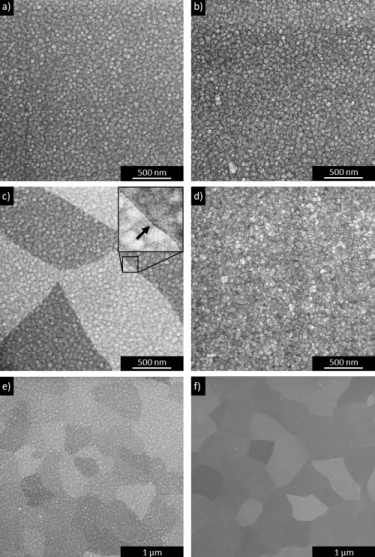
Fig. 1. Top-view SEM images of 100 nm-thick ITO layers on top of reflective back contacts before (a,b) and after (c,d) annealing at 540°C in air for 10 minutes. ITO was deposited (a,c) directly on Ag or (b,d) on a 30 nm-thick ZnO:Al layer sputtered on Ag. Inset in (c): 100 nm × 100 nm region showing a gap at a grain boundary (arrow). (e,f) Annealed 200 nm-thick ITO films deposited (e) on a RBC without ZnO:Al (stack: SLG/ZnO:Al/Ag/ITO) and (f) on SLG (stack: SLG/ITO).
substrate. Ag is used as a metallic reflector, and is encapsulated with ZnO:Al to prevent diffusion during the CIGS co-evaporation process at 500°C. The top layer is made of ITO, as it is expected to provide an ohmic contact with CIGS layers co-evaporated at 500°C [19], [20]. Two different reflective stacks were fabricated, in order to investigate the impacts of the ZnO:Al layer deposited on Ag regarding the optical and electrical properties of complete cells.
After the preparation of reflective back contacts, the morphology of ITO layers deposited on Ag and on ZnO:Al was analyzed before and after annealing. Complete solar cells were then fabricated by direct co-evaporation of 550 nm-thick CIGS on top of Mo and reflective back contacts, respectively. Their performances are measured and compared, and their spectral response is analyzed by means of optical simulations.
II. EXPERIMENTAL METHODS
Ultrathin CIGS solar cells were fabricated on soda lime glass (SLG) substrates with a conventional Mo back contact, and with reflective back contacts made of ZnO:Al/Ag/ITO or ZnO:Al/Ag/ZnO:Al/ITO. 400 nm-thick layers of Mo were prepared by DC sputtering. Flat reflective back contacts (RBC) consist of a 150 nm-thick Ag layer deposited by electron beam evaporation on a 50 nm-thick rf-sputtered layer of ZnO:Al. The Ag layer was then covered by rf-sputtering of a 100 nm-thick ITO layer, or of a ZnO:Al/ITO bilayer stack with respective thicknesses 30nm/100nm. Finally, a 3 nm-thick Al2O3 layer was deposited by Atomic Layer Deposition
(ALD) on top of the reflective stacks in order to limit the formation of Ga oxide at the CIGS/ITO interface [21]. 8 nm-thick NaF precursor layers were evaporated onto each back contact prior to CIGS deposition. Ultrathin CIGS absorbers were co-evaporated simultaneously on each of the three different back contacts using a three-stage process with a
maximum substrate temperature of 500°C. The co-evaporated CIGS layer has an average thickness of 550 nm according to profilometer measurements. Average atomic ratios of [Cu]/([Ga]+[In]) = 0.85 (CGI) and [Ga]/([Ga]+[In]) = 0.39 (GGI) were determined by X-Ray Fluorescence (XRF). Solar cells were completed by chemical bath deposition of a 50 nm-thick CdS layer, followed by rf-sputtering of i-ZnO and ZnO:Al with respective thicknesses of 50 nm and 250 nm.
The morphology of ITO layers sputtered on top of the reflective back contacts and SLG was analyzed by Scanning Electron Microscopy (SEM, FEI) before and after a 10-minute annealing in air at a nominal temperature of 540°C. The CGI, GGI and Mo depth profiles of the CIGS/Mo stack were measured by Glow Discharge Optical Emission Spectroscopy (GD-OES). Home-built systems were used for current-voltage (IV) and External Quantum Efficiency (EQE) measurements. The JSC values reported in this study were derived from the
experimental EQE integrated with the AM1.5G spectrum for each best solar cell.
The optical absorption of complete ultrathin CIGS solar cells were simulated with the Reticolo software [22] using the rigorous coupled wave analysis method. The optical indices of ITO [20] and CIGS were determined from ellipsometric data. Other optical indices used in this study can be found in reference [8]. The thickness of the simulated CIGS layer was fitted to account for the uncertainty of its measurement, and a 500 nm-thick CIGS film was found to provide the best agreement with experimental EQE curves, in accordance with the targeted thickness. Using numerical results, theoretical JSC
values were derived from the absorption calculated in the CIGS layer. JSC losses were calculated by integration of the
parasitic absorption in each other layer for photon energies above the CIGS bandgap of 1.2 eV.
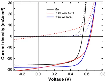
Fig. 3. IV characteristics under one-sun illumination (solid lines) and in the dark (dashed lines) for best solar cells on top of Mo, and reflective back contact (RBC) with and without a 30 nm-thick ZnO:Al layer sandwiched between the Ag and ITO layers.
-0.2 0.0 0.2 0.4 0.6 0.8 -30 -20 -10 0 10 20 30 Current d ens ity (mA/cm²) Voltage (V) Mo RBC w/o AZO RBC w/ AZO
Fig. 2. GD-OES analysis of CGI and GGI depth profiles of ultrathin CIGS deposited on Mo in a 3-stage process.
0 200 400 600 0 20 40 60 80 100 Atomic ratio (%) Sputtered thickness (nm) CGI GGI Mo CIGS Mo
III.RESULTS AND DISCUSSION A. Material Characterization
Fig. 1 shows top-view SEM images of the top ITO layer of reflective back contacts with and without a ZnO:Al layer sandwiched between the Ag and ITO layers, before (a,c) and after (b,d) annealing in air at 540°C for 10 minutes. These stacks should sustain the high temperature of the CIGS deposition process, at least 500°C, with no loss in reflectivity [20] and no silver diffusion through the TCO layers. The annealing in air does not reproduce the exact conditions of the CIGS deposition process, but it provides first indications of the effects of temperature on the stack properties.
Before annealing, the ITO layer is rough, with features smaller than 100 nm. Upon annealing, micrometer-scale grains appear when ITO is directly sputtered on Ag (Figs. 1 (c) and (e)) or on SLG with no Ag (Fig. 1(f). In addition, gaps at grain boundaries are clearly visible in annealed SLG/ZnO:Al/Ag/ITO samples (see arrow in Fig. 1(c)) and may favor the diffusion of silver through the ITO layer.
When an additional ZnO:Al layer is added between Ag and ITO, we do not observe the appearance of grains, and there is no clear morphology changes upon annealing. Hence, the ZnO:Al layer should contribute to the stabilization of the silver layer and to avoid Ag diffusion through the TCO bilayer. These SEM images also indicate that both reflective back contacts do not delaminate at 540°C in air, which is another prerequisite for the direct co-evaporation of ultrathin CIGS.
CGI and GGI profiles of CIGS layers grown on Mo at 500°C were analyzed by GD-OES, as shown in Fig. 2. While the CGI profile is flat in bulk CIGS, it is found that the co-evaporation of ultrathin CIGS in a 3-stage process results in a linear GGI grading. This GGI grading is expected to create a back surface field that helps to passivate the back interface of CIGS [23].
B. Performances of Ultrathin CIGS Solar Cells
The light and dark IV parameters of the fabricated solar cells are summarized in Table 1.
Importantly, the VOC is improved with the reflective back
contacts as compared to the Mo reference. In the case of reflective back contact without ZnO:Al between Ag and ITO, most solar cells are shunted and only the parameters of the best solar cell is reported in Table 1. It exhibits a low fill factor (FF), together with a very low shunting resistance (RSH),
as shown in Table 1 and Fig. 3. This may be due to silver diffusion through the grain boundaries favored by the morphology of ITO shown in Fig. 1. On the other hand, solar cells with a reflective back contact including a ZnO:Al/ITO bilayer exhibit a higher RSH and an average fill factor of FF =
65.1±2.9 %, which is close to the Mo reference with an average FF = 67.5±0.6 %. This indicates that an ohmic contact between CIGS and ITO is achieved, as confirmed by a low series resistance, and that the additional ZnO:Al layer deposited on Ag is necessary to ensure the thermal stability of the full multi-layer stack.
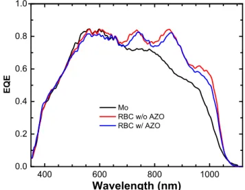
Fig. 4 shows the EQE of best ultrathin solar cells for each type of back contact. Replacing Mo by reflective back TABLE I
SUMMARY OF IV PARAMETERS UNDER AM1.5G ILLUMINATION AND IN THE DARK.AVERAGE VALUES AND STANDARD DEVIATION ARE GIVEN FOR THE 10 BEST CELLS.DARK IV PARAMETERS OF BEST CELLS ARE FITTED WITH A 1-DIODE MODEL (J0: SATURATION
CURRENT, N: IDEALITY FACTOR,RSH: SHUNT RESISTANCE,RS: SERIES RESISTANCE).*FOR THE REFLECTIVE BACK CONTACT
WITHOUT ZNO:AL, LIGHT IV PARAMETERS ARE SPECIFIED FOR THE BEST CELL ONLY BECAUSE OF A STRONG SHUNTING BEHAVIOR IN MOST SOLAR CELLS.
Substrate Light IV parameters (average / best) Best cell dark IV parameter
Eff (%) JSC (EQE) (mA/cm2) VOC (mV) FF (%) J0 (mA/cm2) n RSH (Ω.cm2) RS (Ω.cm2) Mo 9.5 ± 0.1 / 9.7 25.6 549 ± 3 / 553 67.5 ± 0.6 / 68.3 6 E-6 1.5 > 1 E+6 < 0.1 RBC w/o ZnO:Al* 9.6 28.5 644 52.3 4 E-5 2 8 E+1 0.4
RBC w/ ZnO:Al 11.3 ± 0.6 / 12.2 27.8 622 ± 7 / 633 65.1 ± 2.9 / 69.5 5 E-5 2 4 E+3 1.2
Fig. 4. EQE of best solar cells for a Mo back contact, and reflective back contacts (RBC) with and without a 30 nm-thick ZnO:Al layer between the Ag and ITO layers.
400 600 800 1000 0.0 0.2 0.4 0.6 0.8 1.0 EQE Wavelength (nm) Mo RBC w/o AZO RBC w/ AZO
contacts leads to a significant enhancement of the EQE, with large resonances for wavelengths above 700 nm. They result in improved light absorption in ultrathin CIGS layers, and increase the JSC from 25.6 mA/cm2 for the Mo reference to
27.8 mA/cm2 and 28.5 mA/cm2 for reflective back contacts,
with and without ZnO:Al on top of Ag, respectively.
Thanks to a superior rear reflectance and an ohmic behavior, the average efficiency of ultrathin solar cells increased from 9.5±0.1 % with Mo to 11.3±0.6 % for a reflective back contact with a ZnO:Al/ITO bilayer. This back contact led to a best cell efficiency of 12.2%, which corresponds to a 2.5% absolute efficiency enhancement as compared with the best cell with a Mo back contact. However, the best efficiency in the case of a reflective back contact with a single layer of ITO deposited on Ag was limited to 9.6%, due to low FF and RSH.
C. Optical analysis
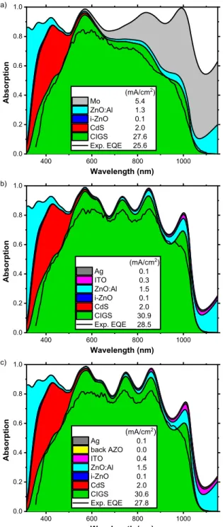
The EQE measured on the three best cells are compared to the results of optical simulations in Fig. 5. Light absorption in each layer of the complete stack of ultrathin CIGS solar cells is plotted (colored regions). The absorption calculated in the CIGS layer is in good agreement with EQE measurements. In particular, the spectral position of the resonance peaks of EQE measurements are accurately reproduced by simulation. EQE spectra exhibit slightly less pronounced peaks. The roughness of the CIGS layers may smoothen the interference effects and results in slightly less pronounced peaks in EQE as compared to calculated spectra.
While a substantial part of the incoming light is absorbed in Mo when it is used as a back contact, reflective back contacts lead to a strong enhancement of CIGS light absorption. For both reflective back contacts a low parasitic absorption is calculated in the ITO layer, and the similar CIGS absorptions indicate that adding a 30 nm-thick ZnO:Al layer on the Ag mirror has no significant impact on light absorption. Theoretical maximum JSC values were calculated by
integrating the simulated CIGS absorptions with the AM1.5G spectrum, assuming perfect collection efficiency. They were improved from 26.9 mA/cm2 on Mo to 30.6 mA/cm2 and 30.9
mA/cm2 on a RBC with and without ZnO:Al, respectively.
These results are close to JSC measurements, indicating a high
internal quantum efficiency.
It is also worth mentioning that the calculated total reflection of solar cells is increased in the infrared region when using a reflective back contact instead of Mo. Firstly, the higher reflection of photons with energy below the CIGS bandgap reduces the operating temperature of CIGS solar cells and has a positive impact on the efficiency and reliability of devices [14]–[18]. Secondly, light absorption in CIGS could be further improved for photon energies above the bandgap by using an additional anti-reflection coating and light trapping structures, for example with a nanostructured back mirror [8], [12], [24].
Fig. 5. Simulated light absorption in each layer of complete ultrathin CIGS solar cells. Back contact is made of a) Mo, b) reflective back contact (RBC) without ZnO:Al on top of Ag and c) RBC with a 30 nm-thick ZnO:Al layer on Ag. Theoretical JSC values
were calculated from the simulated CIGS absorption, as well as the equivalent JSC losses due to the parasitic absorption occurring in
other layers. 400 600 800 1000 0.0 0.2 0.4 0.6 0.8 1.0 Ab so rption Wavelength (nm) (mA/cm2) Mo ZnO:Al i-ZnO CdS CIGS Exp. EQE 5.4 1.3 0.1 2.0 27.6 25.6 a) 400 600 800 1000 0.0 0.2 0.4 0.6 0.8 1.0 Ab so rption Wavelength (nm) (mA/cm2) Ag ITO ZnO:Al i-ZnO CdS CIGS Exp. EQE 0.1 0.3 1.5 0.1 2.0 30.9 28.5 b) 400 600 800 1000 0.0 0.2 0.4 0.6 0.8 1.0 Ab so rption Wavelength (nm) (mA/cm2) Ag back AZO ITO ZnO:Al i-ZnO CdS CIGS Exp. EQE 0.1 0.0 0.4 1.5 0.1 2.0 30.6 27.8 c)
IV.CONCLUSION
Two different architectures of flat reflective back contacts were investigated and used for the fabrication of ultrathin CIGS solar cells with improved light absorption and efficiency. These reflective back contacts include a silver metallic mirror that is covered either with a single layer of ITO or with a ZnO:Al/ITO bilayer. Thanks to the enhancement of the back contact reflectance, a significant increase in EQE and JSC was achieved for both types of
reflective back contacts, in good agreement with optical simulations. Solar cells fabricated on reflective back contacts with ITO sputtered directly on Ag suffer from low RSH and FF.
Reflective back contacts with a ZnO:Al/ITO bilayer on top of Ag were found to be suitable for CIGS co-evaporation and to ensure a good thermal stability of the reflective back contact. They led to a best cell efficiency of 12.2% as well as a JSC =
27.8 mA/cm2, which is respectively 2.5% absolute and 2.2
mA/cm2 more than with a Mo back contact. The architectures
of reflective back contacts described in this work are also compatible with light trapping strategies, and pave the way toward the fabrication of ultrathin CIGS solar cells with complete light absorption in the infrared region.
ACKNOWLEDGEMENTS
The presented work is supported by the ARCIGS-M project, as part of the European Union's Horizon 2020 research and innovation program under grant agreement No. 720887.
REFERENCES
[1] M. Edoff, S. Schleussner, E. Wallin, and O. Lundberg, “Technological and economical aspects on the influence of reduced Cu(In,Ga)Se2 thickness and Ga grading for co-evaporated Cu(In,Ga)Se2 modules,” Thin Solid Films, vol. 519, no. 21, pp. 7530–7533, Aug. 2011.
[2] K. A. W. Horowitz and M. Woodhouse, “Cost and potential of monolithic CIGS photovoltaic modules,” 2015, pp. 1–6.
[3] N. Naghavi et al., “Ultrathin Cu(In,Ga)Se 2 based solar cells,” Thin Solid Films, vol. 633, pp. 55–60, Jul. 2017. [4] Z. J. Li-Kao et al., “Towards ultrathin copper indium
gallium diselenide solar cells: proof of concept study by chemical etching and gold back contact engineering: CIGSe: chemical etching and gold back contact
engineering,” Prog. Photovolt. Res. Appl., vol. 20, no. 5, pp. 582–587, Aug. 2012.
[5] O. Lundberg, M. Bodeg\a ard, J. Malmström, and L. Stolt, “Influence of the Cu (In, Ga) Se2 thickness and Ga grading on solar cell performance,” Prog. Photovolt. Res.
Appl., vol. 11, no. 2, pp. 77–88, 2003.
[6] B. Vermang et al., “Employing Si solar cell technology to increase efficiency of ultra-thin Cu(In,Ga)Se 2 solar cells:
Employing Si solar cell technology,” Prog. Photovolt.
Res. Appl., vol. 22, no. 10, pp. 1023–1029, Oct. 2014.
[7] P. M. P. Salomé et al., “Passivation of Interfaces in Thin Film Solar Cells: Understanding the Effects of a
Nanostructured Rear Point Contact Layer,” Adv. Mater.
Interfaces, vol. 5, no. 2, p. 1701101, Jan. 2018.
[8] J. Goffard et al., “Light Trapping in Ultrathin CIGS Solar Cells with Nanostructured Back Mirrors,” IEEE J.
Photovolt., vol. 7, no. 5, pp. 1433–1441, Sep. 2017.
[9] K. Orgassa, H. W. Schock, and J. H. Werner, “Alternative back contact materials for thin film Cu(In,Ga)Se2 solar cells,” Thin Solid Films, vol. 431–432, pp. 387–391, May 2003.
[10] F. Mollica et al., “Light absorption enhancement in ultra-thin Cu(In,Ga)Se 2 solar cells by substituting the back-contact with a transparent conducting oxide based reflector,” Thin Solid Films, vol. 633, pp. 202–207, Jul. 2017.
[11] B. Vermang et al., “Highly reflective rear surface passivation design for ultra-thin Cu(In,Ga)Se2 solar cells,” Thin Solid Films, vol. 582, pp. 300–303, May 2015.
[12] G. Yin, M. W. Knight, M.-C. van Lare, M. M. Solà Garcia, A. Polman, and M. Schmid, “Optoelectronic Enhancement of Ultrathin CuIn 1-x Ga x Se 2 Solar Cells
by Nanophotonic Contacts,” Adv. Opt. Mater., vol. 5, no. 5, p. 1600637, Mar. 2017.
[13] B. Bissig et al., “Novel back contact reflector for high efficiency and double-graded Cu(In,Ga)Se 2 thin-film
solar cells,” Prog. Photovolt. Res. Appl., vol. 26, no. 11, pp. 894–900, Nov. 2018.
[14] K. Mullaney, G. M. Jones, C. A. Kitchen, and D. P. Jones, “Infra-red reflective coverglasses: the next generation,” in Conference Record of the Twenty Third
IEEE Photovoltaic Specialists Conference - 1993 (Cat. No.93CH3283-9), 1993, pp. 1363–1368.
[15] W. T. Beauchamp, “UV/IR Reflecting Solar Cell Cover,”
US Pat, no. 5 449 413, p. 20, 1995.
[16] H. Yoon et al., “Application of infrared reflecting (IRR) coverglass on multijunction III-V solar cells,” in 2006
IEEE 4th World Conference on Photovoltaic Energy Conference, 2006, vol. 2, pp. 1861–1864.
[17] W. Li, Y. Shi, K. Chen, L. Zhu, and S. Fan, “A Comprehensive Photonic Approach for Solar Cell Cooling,” ACS Photonics, vol. 4, no. 4, pp. 774–782, Apr. 2017.
[18] O. Dupré, R. Vaillon, and M. A. Green, “Physics of the temperature coefficients of solar cells,” Sol. Energy
Mater. Sol. Cells, vol. 140, pp. 92–100, Sep. 2015.
[19] T. Nakada, “Microstructural and diffusion properties of CIGS thin film solar cells fabricated using transparent conducting oxide back contacts,” Thin Solid Films, vol. 480–481, pp. 419–425, Jun. 2005.
[20] L. Gouillart et al., “Development of reflective back contacts for high-efficiency ultrathin Cu(In,Ga)Se2 solar cells,” Thin Solid Films, vol. 672, pp. 1–6, Feb. 2019. [21] J. Keller, W.-C. Chen, L. Riekehr, T. Kubart, T.
Törndahl, and M. Edoff, “Bifacial Cu(In,Ga)Se 2 solar
cells using hydrogen-doped In 2 O 3 films as a transparent
back contact,” Prog. Photovolt. Res. Appl., vol. 26, no. 10, pp. 846–858, Oct. 2018.
[22] P. Lalanne and J. P. Hugonin, “Reticolo software for grating analysis.” [Online]. Available:
https://www.lp2n.institutoptique.fr/lp2n/Membres-Services/Responsables-d-equipe/LALANNE-Philippe. [23] L. M. Mansfield et al., “Efficiency increased to 15.2% for
ultra-thin Cu(In,Ga)Se 2 solar cells,” Prog. Photovolt.
[24] H.-L. Chen et al., “A 19.9%-efficient ultrathin solar cell