Pour l’obtention du grade de
DOCTEUR DE L’UNIVERSITE DE POITIERS Faculté des Sciences Fondamentales et Appliquées
Diplôme National - Arrêté du 7 août 2006
École Doctorale : SCIENCES POUR L’INGENIEUR & AERONAUTIQUE Secteur de Recherche : MILIEUX DENSES, MATERIAUX ET COMPOSANTS
Présentée par
Luc LAJAUNIE
Influence de la préparation de surface sur les propriétés physiques
des contacts à base Cobalt sur n-Ge.
Sous la direction de
Jean-François Barbot et Marie-Laure David Thèse soutenue le 05 Novembre 2009
JURY
P. RUTERANA, Directeur de recherche, CIMAP, Caen Rapporteur
E. SIMOEN Senior scientist, IMEC, Belgique Rapporteur
P. MOREAU, Maître de conférence, IMN, Université de Nantes Examinateur J-F. BARBOT, Professeur, PHYMAT, Université de Poitiers Examinateur M-L. DAVID Maître de conférence, PHYMAT, Université de Poitiers Examinateur T. CABIOC’H Professeur, PHYMAT, Université de Poitiers Examinateur
Voici enfin la dernière touche que je vais apporter à ce manuscrit : les remerciements. C’est normalement ici que je vais poser mon clavier et que vous allez commencer votre lecture (qui va peut-être s’arrêter à la fin de cette page d’ailleurs).
En premier lieu, je tiens à remercier l’ensemble de mon jury de thèse et tout particulièrement Eddy Simoen et Pierre Ruterana qui m’ont fait l’honneur de juger ce manuscript et d’en avoir été les rapporteurs. Je remercie aussi Thierry Cabioc’h et Philippe Moreau d’avoir accepté d’examiner ce travail.
J’adresse mes remerciements tout particuliers à mes encadrant bien-aimés : Marie-France Beaufort (ce fut bref mais intense) Marie-Laure David et Jean-François Barbot pour tous ces bon moments passsés ensemble. Merci à vous pour tout que vous m’avez apporté, tant d’un point de vue humain que scientifique, au cours de ces trois années. Je remercie vivement Fabien Paumier et Sylvie Schamm sans qui ce manuscrit n’aurait surement jamais vu le jour. Je re-remercie Eddy Simoen pour les nombreuses discussions que nous avons eues par mail ou autour d’une bière.
Je tiens également à remercier tous ceux du laboratoire qui m’ont apporté leur aide et leurs conseils au cours de ces trois années : merci à Marc Marteau ainsi qu’a Philippe Guérin pour les dépôts innombrables, à Dominique Eyidi pour sa grande disponibilité à répondre à mes nom-breuses questions concernant la microscopie électronique en transmission, à Christophe Tromas pour les caractérisations par microscopie à force atomique ainsi que pour les discussions qui en ont découlées. Je remercie également Sophie Camélio, Vincent Mauchamp et Karl Opsomer pour le travail que nous avons commencé et qui est exposé dans les perspectives. Merci égale-ment à Yannick Diot, Patrick Tanguy, Jackie Gerbier, Marie-Noëlle Branlé, Fabrice Berneau, Bruno Lamongie et à tous les membres du laboratoire qui participent à cette atmosphère de franche convivialité.
Cyril, Bertrand, Guillaume Geandier, Alex, Amélie, Mathieu. . .
Je finis enfin par l’essentiel: un grand merci à mes parents et à Céline.
Introduction 1
1 Background 3
1.1 Brief overview on silicides . . . 4
1.2 From silicon to germanium . . . 6
1.3 Ge native oxide and cleaning of Ge surfaces . . . 8
1.4 Germanides and Cobalt Germanides . . . 9
1.5 Schottky barrier height on n-type Ge and Fermi level pinning . . . 10
1.6 Conclusion . . . 13
2 Experimental procedure and theoretical background 15 2.1 Sample process . . . 16
2.1.1 Pre-treatment procedures . . . 17
2.1.2 Electron beam physical vapor deposition . . . 18
2.1.3 Post-metal deposition annealing . . . 19
2.2 Sample characterization . . . 20
2.2.1 sample preparation for TEM observations . . . 21
2.3 Electrical characteristics . . . 21
2.3.1 Schottky contact . . . 22
2.3.2 C-V characteristics . . . 23
2.3.3 I-V forward characteristics . . . 26
2.3.4 Extraction of SBH from C-V or I-V characteristics ? . . . 30
2.3.5 I-V reverse characteristics . . . 31
2.3.6 Deep-Level Transient Spectroscopy (DLTS) . . . 33
3.1.1 Reference sample . . . 40
3.1.2 Pre-treated samples . . . 42
3.2 Electrical characterization: general considerations . . . 43
3.2.1 C-V and I-V forward measurements at a fixed temperature: 160 K . . . . 43
3.2.2 Study of the deep level traps . . . 46
3.2.3 I-V reverse characteristics . . . 49
3.3 C-V-T and I-V-T measurements: inhomogeneous SBH . . . 52
3.3.1 Measurements at different temperatures (80-270K) . . . 52
3.3.2 SBH inhomogeneities: the model of Werner and Güttler (WG model) . . 56
3.3.3 Voltage dependencies of the Gaussian parameters . . . 59
3.3.4 SBH inhomogeneities: results . . . 63
3.4 Conclusion . . . 66
4 Annealed samples : electrical properties and microstructure 67 4.1 General remarks . . . 68
4.2 Microstructural characterization: TEM and AFM analyses . . . 69
4.2.1 Microstructural characterization of the single layer structure (P 400A sample) . . . 71
4.2.2 Microstructural characterization of the double layer structure (REF A, P HF Aand P 700A samples) . . . . 74
4.2.3 Summary . . . 84
4.3 Electrical characterization . . . 85
4.3.1 Study of the DLTS traps after germanidation . . . 85
4.3.2 I-V reverse characteristics . . . 86
4.3.3 Determination of SBH inhomogeneities: . . . 88
4.4 Conclusion . . . 96
5 Summary and Discussion 97
Prospects 105
Annexe 109
Since the 1960s, silicon based devices dominate the world market of electronic devices. In the beginning of the 21th century, it is still dominated by silicon and is likely to remain so far at least another decade since no other semiconductor can compete in terms of material quality. At the moment the other semiconductors only fill niche applications such as light emission (GaAs for example) due to its indirect bandgap or high temperature environment (SiC for example) due to its "small" width of bandgap.
This situation could also change in Complementary Metal Oxyde Semiconductors (CMOS) technology for which channel mobility is a major challenge to meet the requirements of sub-22 nm device geometries. The materials that could replace the well-established silicon are strained silicon and germanium. Let us remind that silicon has been favoured over Ge primarily because of the higher quality native oxide possessed by Si.
Ge technology is clearly not really as mature as silicon, and it is more expensive than silicon, but its high electron and hole mobility make it a potential candidate and provides a strong driving force for its development and implementation. Ge has recently attracted more considerable attention due to high-k dielectric materials. Now, considerable efforts are put toward Ge wafer fabrication and device development by semiconductor industries. One of the challenges in such electronic device applications is the control of metal contact properties. These properties of the metal/Ge interfaces include uniformity and thickness of interfacial region, stability, and most importantly, the Schottky barrier height (SBH), or the energy barrier for electrons going through the interface. The SBH determines the electrical behavior of an ohmic or Schottky contact. A low SBH is necessary to create good ohmic contacts while a large SBH is required for good rectifying contact. Because of the critical importance of the SBH, much research has been devoted to achieve and to understand the underlying phenomena. Indeed, if the Schottky Mott equation suggests that the SBH is only achieved by the choice of a metal, it is, in practice, never the case (surface effects, surface states). In certain cases (large density of surface states), the Fermi level is said "pinned" and the barrier height control is lost. The
structure of the interface is thus important in terms of interface states, which in turn affects the variability of the barrier height. Therefore the preparation of a clean semiconductor surface is vital to the resulting contact properties.
Similar to the case in a Si-based CMOS transistor where self-aligned metal silicide layers are used, self-aligned metal germanides will be used as contact materials in the future Ge-based MOSFET structures as well. The use of self-aligned germanides for contact metallization and local wiring is a response to the continued decreasing of the MOSFET structure size that re-quires minimized parasitic contact and series resistances in the gate and source/drain regions to enhance the device speed. In the same way, as in silicon, metals which can be used in Ge are for example Ni, Co and Ti.
In this work we report on the observations of Co-germanide SBHs formed on n-type Ge substrates and discuss the current mechanisms. Notable results were already reported for cobalt germanides and the formation of CoGe2, Co5Ge7 were studied in detail. However, many factors
are known to affect Schottky barrier height in rectifying contacts, one of them concerns the control of the surface preparation prior to metal deposition (quality of the metal/semiconductor interface). Consequently, we chose to study the formation of SBHs by the Co germanidation on Ge substrates that have undergone various surface treatments (annealing in vacuum or HF pre-treatment). A detailed analysis of the temperature dependence of the diode characteristics has been carried out to understand the large underestimation of the Richardson’s constant. The results have been discussed in terms of barrier inhomogeneity. These electrical results have been also analyzed and compared to the microstructure of contacts that have been studied by using transmission electron microscopy. Both characterizations, electrical and structural have been conducted in parallel. Capacitive spectroscopy measurements were also carried out to determine the metallic diffusion or the contamination of metallic species during various phases necessary to the elaboration of the Co-based Schottky contact.
The manuscript is written in the following way. In the first chapter we remind some gener-alities and previous studies which will be useful for the understanding of our work. The second chapter describes the experimental procedure which we used and presents also some theoretical backgrounds on the formation and on the characterization of contacts. Both following chapters are the key chapters of this study; the chapter 3 presents and discusses the results obtained on as-deposited samples while the chapter 4 presents those obtained after annealing, i.e. after Co-germanidation. Finally the results are summarized and some perspectives of this work are presented.
Background
In this first Chapter, the role played by Ge in the microelectronic industry is reminded. One of the crucial element in the elaboration of devices, whatever they are, is the Ohmic and Schottky contacts. The cleaning of the surface and the germanidation are also main parameters in the elaboration of successful components. Some previous useful studies for a better understanding of our work will thus be described. Finally, the Schottky barrier height and the Fermi level pinning due to the weak dependence of the Schottky barrier height on the metal work function are also approached.
1.1
Brief overview on silicides
Figure 1.1: A cross-section
transmis-sion electron microscope image of a 0.1
µm (gate lenth) T iSi2 salicide structure,
taken from [1].
Figure 1.2: Schematic of a cross-section of
a MOS devices.
Silicides were introduced as early as the 1960s for ohmic and rectifying contacts to silicon and nowadays they become an indispensable technique for high-performance CMOS (Complemen-tary Metal Oxide Semiconductor) fabrication. They are used to lower sheet resistance of gate and source-drain regions in the CMOS technology in order to increase the device performances. Today most silicides are formed by the self-aligned process (SALICIDE) introduced more than 20 years ago [2]. As example, Fig. 1.1 and Fig. 1.2 illustrate the use of silicides in the MOS devices used at present in CMOS technology.
Figure 1.3: SALICIDE process flow, from [3]
Fig. 1.3shows the SALICIDE process flow for Co and Ti silicides [3]. The first step consists of the deposition (sputtering in general) of the metal onto the future MOSFET. In the second
step (silicide formation step), the deposited metal film is thermally reacted to form the silicide films on gate and source/drain areas. In the third step, unreacted metal films are removed by selective etching, leaving silicide films on gate and source/drain areas. Finally, another thermal step at a higher temperature is used to transform the silicide films into the wanted low-resistivity phase.
Since the beginning of mid 80s, the most common used silicide has been T iSi2, with the
crystallographic notation C54 and which presents a low resistivity of 15-25 µΩ.cm. However, another phase of high resistivity (60-80 µΩ.cm) has been found to be more stable than C54 in restricted geometries, rendering thus, the Ti silicidation incompatible with the scaling down of electronic devices [2].
The successors of T iSi2 are CoSi2 and NiSi which both present similar resistivity than T iSi2
but overcome the small geometry problem. However, further research is still necessary for further scaling. One of the difficulties in implementing a Co silicide process resides in the opti-mization of the cleaning of the Si substrate: the microstructure of Co silicides being much more sensitive to the presence of native oxide (and also residual oxygen in the annealing chamber) than Ti silicides [4]. On the other hand, the NiSi silicide presents a high temperature degra-dation of the morphology of the thin film upon annealing referred to as agglomeration [5]. The agglomeration process describes the trend of silicides to be discontinuous upon annealing as illustrated by Fig. 1.4. However, the introduction of impurities inside the Si substrate before silicidation has been shown to delay such agglomeration and extending thus the temperature window for further processing of a Ni silicide MOSFET NiSi [6,7].
Figure 1.4: TEM images illustrating the agglomeration of NiSi thin film upon annealing, taken
From all these observations, some of key considerations for the application of silicides (and germanides) as source/drain contacts come out: [4, 8,9]:
• low sheet resistance
• low formation temperature
• etch selectivity of the silicide versus the metal (allows self-aligned process) • good thermal stability
• low contact resistivity
• good scalability (formation in small structures) • good uniformity, low interface roughness
• low metal diffusion into the substrate.
1.2
From silicon to germanium
Figure 1.5: First transistor (made of Ge) invented at Bell Labs on December 23, 1947 by Bardeen
and Brattain, taken from [10].
Since the first transistor was introduced [11], Ge has been considered as one of the most im-portant semiconductors. However due to the better physical and chemical properties of silicon dioxide than Ge oxide, Si has been the main material in CMOS devices for decades. For in-stance, SiO2 can be thermally grown on Si substrate while Ge oxide desorbs upon annealing [12].
However, the constant reduction of the physical oxide thickness imposed by the scaling challenges, has required the shift of SiO2 toward high-κ dielectrics [13]. This shift puts the
dominant role of Si as the major material into question and renews the interest for high-mobility substrates like Ge. Comparatively to Si, Ge offers a 4 and 2 times higher mobility for holes and electrons [14] respectively, allowing thus to theoretically achieve higher device performance. Moreover, with the use of high-κ dielectric materials, the instability of germanium oxide is now an advantage: the removal of interfacial oxide can be readily achieved (see Fig. 1.6) more easily than high-k/Si system [15]. This potential advantage of high-k/Ge system has been demon-strated by several experimental results [12].
Figure 1.6: Cross-sectional TEM image (X-TEM) of a high-κ dielectric on Ge. No interface layer is
observed, taken from [16].
However further studies are still needed for the implementation of Ge material in the CMOS technology, especially for Ge MOSFETs which have shown lesser performance than Si n-MOSFETs [17]. To achieve better performances on n-MOSFETs, several issues like the poor dopant activation have to be resolved. The realization of Ge metal source/drain MOSFETs (MSD MOSFETs) which overcomes the dopant activation problem is seen as a promising solu-tion [17]. Encouraging results have been shown for MSD p-MOSFETs [18, 19], however, as it will be discussed later, some difficulties arise for the realization of MSD n-MOSFETs onto Ge.
1.3
Ge native oxide and cleaning of Ge surfaces
To make high performance devices in Ge, it is essential to understand the Ge surface chemistry. Cleaning and passivation of Ge surfaces have been extensively studied for high-κ dielectrics inte-gration in germanium metal-oxide-semiconductor field effect transistors (MOSFETs). However they are few studies on their influences on the properties of Schottky contacts [12]. The native Ge oxide is polymorph and is formed mainly of GeO2 and GeO structures and other suboxides
(GeOx, x < 2) [12, 20, 21]. In addition to be highly toxic for the human beings and the envi-ronment, some authors reported that a certain amount of germanium suboxides remains after HF pre-treatment [22, 23]. However this amount of suboxides can be decreased by increasing the concentration to a ratio higher than 1/5 [23]. In order to remove GeOx, solutions including several cycles of oxidizing agent, such as H2O2 to oxidize the suboxide, and HF have been
tested [24]. In pure N2 atmosphere, passivation of the dangling-bonds of Ge surface by
Hydro-gen after an HF pre-treatment is stable for at least 12h [25] while in ambient air it is estimated to fifteen minutes [26]. On the other hand, a comparisons between HF and HCl pre-treatments has shown that the roughness of the germanium surface increases by a factor 2 with HF [23] and that, contrary to HCl, the metal impurities at the Ge surface do not decrease after an HF pre-treatment [27]. It is noteworthy that, in most of the studies concerning the character-ization of Schottky barrier heights on Ge, HF etching is the most used cleaning method [28–30]. The main difficulties for efficient Ge cleaning is that the several germanium oxides have different responses to pre-treatments. For instance, GeO2 is soluble in water while, in contrast,
GeO is insoluble [12]. Another way to clean the germanium surface is to realize the thermal decomposition of the oxide layer. Prabhakaran et al. performed a study on the thermal decom-position of ultrathin Ge (100) oxide layer by synchrotron radiation photoelectron spectroscopy in ultrahigh vacuum [20]. They reported that during annealing the signal of GeO2 decreases
while the signal of GeO increases (it is noteworthy that from their experiments GeOx can not be distinguished from other suboxides), according to the following reaction :
GeO2(s) + Ge(s) → GeO(s) (1.1)
The left hand side of Eq. 1.1 indicates that GeO2 consumes Ge at the interface to form
GeO. This reaction is followed by the complete desorption of GeO(s) into GeO(g) (GeO(s) → GeO(g)) at 430°C leading thus to the formation of a clean Ge surface. However some authors
reported that heating in UHV at 360°C during 15 minutes is enough to obtain an oxide-free Ge surface [31]. Discrepancies are thus observed in the literature concerning the desorption temperature.
1.4
Germanides and Cobalt Germanides
Similar as self-aligned silicides in Si-based CMOS technology, germanides are considered in Ge (and SiGe)-based CMOS technologies. As mentioned above, the fundamental requirement for the application of germanides into the CMOS technology is the formation of a low-resistivity phase.
To select the promising candidates, Gaudet et al. performed a systematic study of the thermally induced reaction of 20 transition metals with Ge substrate [32]. During annealing, they monitored in-situ the appearance of phases by X-ray diffraction (XRD) and the sheet resistance was determined by ex-situ electrical measurements on quenched samples by the four point probe method. A large group of transition metals was excluded as they did not match the criteria (no reaction with Ge, strong sensitivity to oxidation and high sheet resistance). Among the 20 transition metals, six promising candidates were proposed: Fe, Co, Ni, Pd, Pt and Cu.
Gaudet et al. determined also the phase formation sequence of Co germanides. Indeed, like cobalt silicides, thin films of cobalt germanides formed by solid-state reaction follow a de-fined sequence of phases appearance with increasing annealing temperature : monoclinic CoGe, tetragonal Co5Ge7 and orthorhombic CoGe2, the Ge-rich cobalt germanides being found at high
temperature. This sequence of phase formation was also confirmed by other groups [33–37]. For instance, rapid thermal annealing of a 30 nm cobalt thin film onto a Ge substrate shows that a single-phase of CoGe forms at 300°C while Co5Ge7 appears at 450°C [37]; these two
phases coexist in the temperature range 450°C-550°C. Further annealing at 700°C leads to the full conversion of Co5Ge7 into CoGe2. All the germanide films formed are polycrystalline.
The coexistence of Co5Ge7 and CoGe2 was also highlighted near the transition temperature
of Co5Ge7 into CoGe2 [34]. However if the sequence of apparition of cobalt germanide thin
films is well-defined, a strong discrepancy onto the temperatures of transition is observed in the literature. The crystallinity of the germanium substrate was shown to strongly influence
these temperatures of transition [36]. Moreover, the impact of the conditions of deposition and annealing onto these temperatures of transition can not be ruled out.
Another requirement is the low metal diffusion into the substrate during germanidation. Indeed transition metals in Ge can strongly impact the devices performances by acting as re-combination centers, lifetime killers and leakage current generators [38]. It was shown by Deep Level transient Spectroscopy (DLTS) on n-type Ge that metal in-diffusion occurs in the Ge substrate during Fe, Co and Ni Germanidation [9, 39, 40]. Moreover, Fe and Ni are the most efficient lifetime killers in n-type Ge at room temperature [38]. However, for low-temperature germanidation (400°C-500°C, depending on the metals) metals in-diffusion can be limited with-out any detrimental impact on electronic devices [39]. Furthermore, the temperature of ger-manidation has to be kept below 600°C to avoid cross-contamination with fast diffusers (Cu, Ni). Comparatively to silicides, few studies were carried out on germanides. However according to the first studies on nickel germanides, some difficulties arise. Like nickel silicide, nickel germanides were found to be prone to agglomeration close to 500°C on bulk Ge [29]. However, some solutions like the addition of ultrathin Ti layer to retard the temperature of agglomeration are currently investigated [29]. Moreover, it will be difficult to isolate the low-resistivity wanted phase (NiGe according to [32]) as Ni5Ge3 and NiGe have been found to grow simultaneously
on amorphous Ge and (001) Ge substrates [41–43]. According to Gaudet et al., the wanted low-resistivity phase in Co/Ge system is CoGe2 with a resitivity of 69 µΩ.cm (35 µΩ.cm in [34]).
However according to their results, the resistivity of Co5Ge7 should be similar and presents the
benefit of low-Ge consumption and low-temperature of phase formation (and therefore lower metal in-diffusion in the Ge substrate).
1.5
Schottky barrier height on n-type Ge and Fermi level
pinning
Germanides have been reported as promising source/drain materials for Ge metal source/drain p-MOSFETs (MSD MOSFETs) [18, 19]. However to achieve high performances on MSD n-MOSFETs the Schottky barrier height (SBH) for electrons must be small and that for holes must be large [17]. In an ideal case, the SBH for electrons (φB) depends on the metal work function (φm) and semiconductor affinity (qχs= 4 eV at 300K for Ge [44]) according to:
φB = φm− χs (1.2) Therefore, in theory, it should be possible to tailor the SBH for electron by choosing the appropriate metal. In annexe, most of the SBH measured on n-type Ge are listed. The most striking feature of these tables is that, whatever the metal, the direct contact metal/n-Ge yields to high SBH between 0.5 and 0.6 eV. However, it is not straightforward that the different meth-ods (I-V forward measurements, C-V measurements, Arrhenius plots) used to determine the SBH are comparable, as it will be discussed in the next chapters.
This weak dependence of the SBH on the metal work function is a phenomenon known as Fermi level pinning: the direct contact Metal/n-Ge yields the Fermi level (FL) of the metal to be pinned toward the valence band of Ge and thus, yielding a high SBH (see left hand side of Fig. 1.7) [31, 45].
Figure 1.7: Schematics of the band diagram of a) a strongly pinned Schottky contact and b) a
pinning-alleviated contact by insertion of a thin tunneling oxide, taken from [28].
Even after many years of research, the FL pinning is still subject to debate. According to the metal induced gap states (MIGS) theory, the FL pinning is due to the wave function of the metal penetrating into the semiconductor and inducing additional states in the band gap [46]. However, a recent work of Tung points out the role of the dangling bonds at the metal/semiconductor interface [47]. In many of the models concerning the FL pinning, the SBH for electron is given by [46]:
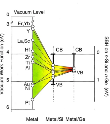
φB = S(φm− φCN L) + (φCN L− χs) (1.3) where S is the pinning factor (0.005±0.001 for Ge [31]) and φCN Ldefines the energy position (with respect to the valence band) around which the FL is pinned (φCN L=0.09±0.07 eV for Ge [31]). This pinning effect is much stronger in Ge than in Si as illustrated by Fig. 1.8.
Figure 1.8: Schematic illustrating the stronger pinning in Ge near the valence band compared to Si;
CB : conduction band, VB: valence band, taken from [46]
However, by introducing a thin oxide layer at the metal/Ge interface, the Fermi level can be depinned (see right side of Fig. 1.7) [17, 28], i.e the FL of the metal is released toward the conduction band of Ge, thus yielding a lower SBH. For instance, by inserting a thin layer (2nm) of Al2O3 at the metal/semiconductor interface, SBH of Co/n-Ge diodes has been found
to decrease from 0.62 to 0.35 eV [28]. The depinning efficiency of the oxide, is dependent on the nature of the metal [28], but also on the thickness and on the chemical nature of the oxide [17]. By implanting sulfur ions before metal deposition, alleviation of Fermi Level pinning (from 0.61 to 0.15 eV) has also been reported on Nickel germanide [48].
It is noteworthy that SBH larger than the Ge band gap have been reported with Ni and Pt germanides [49,50] suggesting the formation of an inversion layer at the interface Metal/Ge. A recent work of Tsipas and Dimoulas has shown that, as the Ge band gap is small and the charge neutrality level lies close to the valence band, the Ge surface tends to be p-type, irrespective of the bulk conductivity [51].
1.6
Conclusion
Due to its high carrier mobility and the promising results obtained in the fabrication of high-κ dielectrics, Ge becomes an attractive material to replace Si in the CMOS technology. As in the conventional Si technology where self-aligned metal silicide is used for gate, source/drain con-tacts, germanidation must be also controlled for Ge device applications. Moreover, to enhance the development of Ge-based metal source/drain MOSFETs, further fundamental researches are needed to overcome the limitation due to Fermi-level pinning in Ge.
So, in our work the Co germanidation has been studied by using different cleaning surface procedures. The electrical properties of such Schottky diodes have been studied with regards to their microstructure.
Experimental procedure and
theoretical background
The first section of this chapter outlines the different pre-treatment procedures tested in this work. The second presents the technique of electron beam deposition (EBD). This part is followed by the description of the Transmission Electron Microscopy (TEM) sample preparation. Then, the chapter ends in a brief overview of both, the general electrical characteristics of Schottky contacts and the Deep Level Transient Spectroscopy (DLTS) technique.
2.1
Sample process
Figure2.1shows the overall process used to prepare the samples. N-type (001) germanium (14 ≤ ρ ≤23 Ω.cm) wafers from UMICORE have been used. After different surface preparations (pre-treatment) that will be detailed in the following, a 22 nm thick cobalt film has been deposited via an electron beam deposition system. For each run, two samples were mounted in the deposition chamber: one sample was dedicated to the microstructural characterization (TEM and AFM mostly) whereas the second was given over to electrical characterization. The Co film has thus been deposited on either the entire sample or through a 2 mm diameter mask (see Fig. 2.2). Some of the samples have then been annealed in-situ to avoid the thin film oxidation before germanide formation.
Figure 2.2: Co diode on n-type Ge.
2.1.1
Pre-treatment procedures
As discussed in detail in Chapter 1, HF etching is the method which is mostly used to prepare germanium or silicon surfaces prior to the Schottky contact formation i.e the metal deposition [9, 36, 49, 52, 53]. However, others methods such as thermal pre-treatment have also been proposed. In particular it has been reported that an annealing at 300°C during 25 min is suffi-cient to remove the germanium oxide [54]. In this study, the influence of the pre-treatment on the electrical properties of Schottky contact has been studied. Three pre-treatments have been investigated, the procedures are summarized in Table 2.1.
Sample Chemical pre-treatment Thermal pre-treatment
REF X X PHF acetone ethanol HF (4%) X deionized water ethanol Dry: N2 air
P400 X 400°C, 40 minramp: 20 min P700 X 700°C, 40 minramp: 20 min
Table 2.1: Pre-treatment procedures used before the Co deposition.
• Reference sample (REF): the reference sample has not been submitted to any pre-treatment. A freshly open piece of germanium wafer has been loaded in the deposition chamber.
• HF etching (PHF): the sample has been dipped successively in acetone and ethanol solu-tions and thereafter submitted to an HF etching (4%) during 30 seconds. This has been followed by 3 rinces in deionized water and one rince in an ethanol solution. Then, the germanium substrate has been dried under N2 air and loaded in the deposition chamber.
As the passivation by hydrogen of the germanium surface is estimated to be 15 minutes in air [26], great care has been taken to act as fast as possible. However we cannot disregard the possibility that few atomic layers of oxide has been formed during the process (time to load the samples in the deposition chamber under a pressure of 10−8torr ∼ 5 min).
• Thermal pre-treatments (P400 and P700): two temperatures of pre-treatment have been chosen : 400°C and 700°C. The temperature ramp as the duration of the pre-treatment were the same for the two thermal pre-treatments (respectively 20 and 40 min). After the pre-treatments, several hours were necessary to reach room temperature before the cobalt deposition could take place. This is of particular importance as cobalt is found to react with germanium at low temperature: at 300°C, according to [36], the formation of CoGe phase has been observed by XRD during germanidation.
2.1.2
Electron beam physical vapor deposition
Cobalt thin films with a constant thickness of 22 nm were deposited on the germanium sub-strates by Electron Beam Deposition (EBD) often called Electron Beam Physical Vapor De-position. The EBD principle is outlined on Figure 2.3. The post-deposition annealing was performed inside the deposition chamber under high vacuum. This is more detailed in the following. The deposition chamber is evacuated to a pressure of 10−8 torr. Electron beam is
generated by thermionic emission of a tungsten filament submitted to a current of nearly 70 A. The electron beam is accelerated by the difference of potential (9 kV) between the filament and the anode (the crucible). A magnetic field perpendicular to the plane of the Fig. 2.3 shifts the electron beam to the cobalt target embedded in a copper crucible. Before each deposition, the target is pre-evaporated during 30 seconds while the samples are protected by the shutter to get rid of the possible oxidation of the target. During the evaporation, the crucible is water-cooled to avoid copper contamination. Moreover, the double walls of the deposition chamber are filled with liquid nitrogen allowing the pressure to be maintened at 10−8 torr during the
deposition. The thickness of the thin film is controlled by a quartz crystal thickness monitor. The deposition rate of the cobalt thin films is estimated to be 0.05 Å/s.
Figure 2.3: Principle diagram of electron beam deposition, taken from [55].
Annealing (and thus the thermal pre-treatments) can be performed in-situ by four lamps of 2000 Watts located in the vicinity of the sample holder. The maximum reachable temperature is nearly 900°C. Under annealing, the pressure of the chamber rises up to 10−6 torr. At such
pressure the germanium and cobalt vaporisation temperatures are respectively 950 and 1100 °C. As the maximum temperature used in this work is 700°C, Co/Ge samples can not be vaporized during annealing.
2.1.3
Post-metal deposition annealing
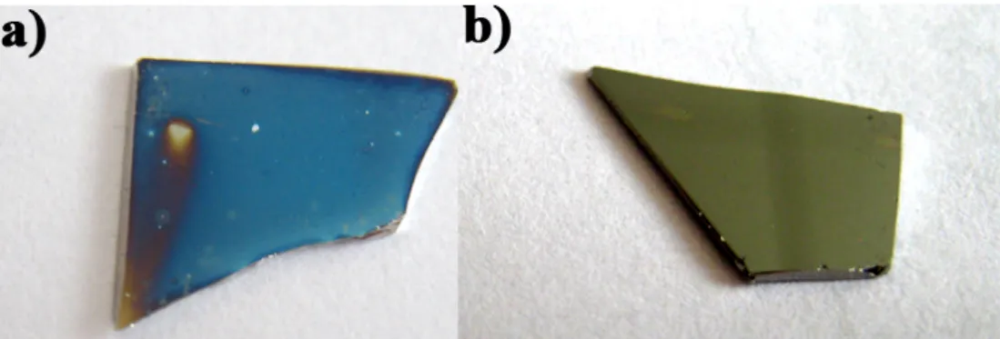
At the early beginning of this work, severals trials of post-metal deposition annealing were performed in a horizontal furnace. The pressures before and during annealing were respectively 10−6 torr and 10−9 torr. After annealing, the sample surfaces present an unusual color as shown
in Fig. 2.4 due to the thin cobalt film oxidation. Cobalt thin films are very sensitive to the oxygen contained in the annealing atmosphere. This is well known from the microelectronics industry since the CoSi2 introduction in the silicide technology [4].
Figure 2.4: a) Sample annealed in horizontal furnace. b) samples annealed in the EBD chamber.
To avoid this, the post-metal deposition annealing was later performed inside the EBD chamber. Regarding the high level of vacuum inside the chamber, the EBD system revealed itself as a very powerful tool as the deposition, the pre-treatment and the post-metal deposition annealing can be performed in a row without exposing the sample to the air. The germanidation process was achieved by thermal diffusion of cobalt at a temperature of 700°C during 40 min (ramp: 20 min). The nomenclature of the samples after post-metal deposition annealing is given in Tab. 2.2.
As deposited sample Annealing procedure Annealed sample REF
700°C, 40 min (ramp: 20 min)
REFA
PHF PHFA
P400 P400A
P700 P700A
Table 2.2: Nomenclature of the samples before and after thermal annealing.
2.2
Sample characterization
Before and after post-metal deposition annealing, the samples have been characterized by dif-ferent techniques such as Transmission Electron Microscopy (TEM), X-ray diffraction (XRD), Atomic Force Microscopy (AFM), electrical characterizations (C-V and I-V) and Deep-Level Transient Spectroscopy (DLTS). In this section, the three main used techniques are briefly described: TEM sample preparation, electrical characterizations and DLTS.
2.2.1
sample preparation for TEM observations
To be observable by a transmission electron microscope, the thickness of the samples has to be less than one hundred nanometer. The goal of the sample preparation is to decrease severely the thickness without affecting the nature of the sample during the process. There are two distinct ways to cut the samples: the plan-view and the cross-section. During the TEM obser-vation, the electron beam is normal to the interface thin film/substrate in the case of a plane view (Fig.2.5.a) and parallel (Fig.2.5.b) to the interface for a cross section. Compared with the plan-view, the cross-sectionnal TEM observation is more favorable for obtaining microstruc-tural informations since thin films often grow coherently on the substrate with preferential orientation. All our samples have been studied in the cross-section geometry (X-TEM).
Figure 2.5: Diagram of plan-view (a) and cross section (b) geometries. The thin film is in red and
the substrate in gray.
Once cut, the TEM sample preparation is divided in two parts : the mechanical polishing and the ion beam thinning. During the mechanical polishing, the samples are downsized to few micrometers by using abrasive SiC discs and a tripod. Thereafter, the sample is glued to a copper grid and thinned by two ionic Argon guns. The energy of the Argon ions was kept to 2.5 keV to avoid amorphization of the substrate. In a same approach, the milling angles were kept to 7° to avoid the impact of the Ar ions on the copper grid and so circumvent the copper contamination of the samples.
Most of the TEM observations have been performed by using a JEOL 3010 TEM (LaB6,
300 kV, point to point resolution 1.9 Å)
2.3
Electrical characteristics
The electrical characterizations (C-V, I-V and DLTS measurements) of the diodes have been performed using a DL8000 Biorad apparatus with a He cryostat allowing a temperature vari-ation from 40 to 350K with a temperature sensitivity of 0.1 K. For this purpose, the area of each diodes has been determined by using an optical microscope allowing then an accurate
determination of electrical parameters.
After a general introduction about Schottky contacts, the two main ways to determine the Schottky barrier height (SBH) is presented. The SBH can be derived from either the C-V or the I-V characteristics. A comparison between these two techniques can be useful to appreciate the quality of Schottky contacts [56–58].
2.3.1
Schottky contact
Figure 2.6: a) Energy band diagram of a metal adjacent to a n-type semiconductor, b) Energy band
diagram of metal-semiconductor contact in thermal equilibrium, taken from [59] .
Fig. 2.6a shows the energy band diagram of a metal adjacent to a n-type semiconductor. The work function is the energy difference between the Fermi level and the vacuum level (i.e qφm for the metal and qφs for the semiconductor). Also shown is the electron affinity qχ, which is the energy difference between the conduction band edge and the vacuum level in the semicon-ductor. A Schottky contact is achieved when the work function of a n-type semiconductor is
less than the work function of the metal (qφs < qφm).
When the metal and the semiconductor make intimate contact, electrons pass from the semiconductor into the metal and the two Fermi levels are forced into coincidence as shown in Fig. 2.6b. There must be a negative charge on the surface of the metal balanced by the positive charge in the semiconductor. Since the semiconductor is of n-type, the positive charge will be provided by conduction electrons receding from the surface leaving uncompensated donor ions in a region depleted of electrons. Because the donor concentration is many orders of magnitude less than the concentration of electrons in the metal, the uncompensated donors occupy a layer of appreciable thickness W. This region, free of electrons, is called space charge region (SCR), and will be noted W in the following. The barrier height to the Fermi level is defined as: Eb = qφB = q(φm− χ). The barrier which prevents the electrons of passing from the semiconductor to the metal is given by: qVbi = q(φm−φs), where Vbi, is the built-in potential.
2.3.2
C-V characteristics
When the Schottky diode is polarized under a reverse bias, VR, the thickness of the SCR is given by: W(VR) = s 2εε0A qND (V bi− VR) (2.1)
where ε is the permittivity of the semiconductor (εGe=16.5), ε0is the vacuum permittivity, A
the area of the contact and ND is the free carrier concentration. In the case of a semiconductor with a negligible defect concentration, the free carrier concentration is equal to the doping concentration (n=ND). As the SCR is free of electrons, the contact is similar to a plane capacitor where the SCR, of thickness W, is the insulator. The capacitance is thus given by :
C(VR) =
εε0A
W(VR)
(2.2) If the doping concentration is uniform, the free carrier concentration can be deduced from the slope of the curve 1
C2 = f(VR) and the built-in potential from the y-intercept of this curve (see Eq. 2.3).
A2 C2 = ( 2 qεε0ND )(Vbi− kT q − VR) (2.3)
Figure 2.7: Experimental C=f(VR) and C12 = f(VR) curves from a Co/Ge Schottky diode at 130K
with the contact area A = 3.14 × 10⁻² cm2. The deduced parameters are ND = 8.9 × 10¹³ at/cm3
and Vbi= 0.50 V
For instance, the C(VR) curve of a Co/Ge Schottky diode is shown Fig. 2.7 and the C12 =
f(VR) is shown in the inset. The barrier height can then be obtained from [59] :
qφCVB = q(Vbi+ kT q + EC − EF q ) = q(Vbi+ kT q + kT q ln NC ND ) (2.4)
where NC is the effective density of states in the conduction band (NC = 2.5×10¹⁹(m
∗ me) 3 2( T 300) 3 2 =
1.2 × 1018 cm−3 at 130 K). In the case of the example, qφCV
B = 0.63 eV.
If a thin insulator is present at the interface, the structure is similar to two series capacitance, one resulting from the presence of the insulator (Cox) and the other from the space charge region of the semiconductor [59]. The apparent capacitance Capp is then given by :
1 Capp = 1 CSC + 1 Cox (2.5)
with
CSC(VR) =
εSCε0A
W(VR)
and
Cox = εoxε0
tox (2.7)
where W (VR) is the width of the space charge region, εox and tox are respectively the permittivity and the thickness of the insulator. By comparing the order of magnitude of these capacitances for a structure Co/GeO2/Ge with an insulator thickness equal to 2 nm
(observed thickness of the germanium native oxide in reference sample, see the following), it comes CSC ≈ 1 × 10⁻¹⁰ F.cm−2 (εGe = 16.5, VR = −5 V and ND = 1 × 1014 cm−3) and Cox ≈ 3 × 10⁻² F.cm−2 (εGeO2 = 6, recently reported values are between 5 and 7 [60, 61]).
The capacitance resulting of the presence of the oxide is several order of magnitude larger than CSC. Therefore, the capacitance of the structure is equal to the capacitance resulting from the space charge of the germanium :
Capp≈ CSC (2.8)
In conclusion, a thin oxide layer does not affect the C(VR) curves in the high frequency regime (f=1MHz; capacitance bridge).
2.3.3
I-V forward characteristics
The case of an ideal Schottky contact
Three main transport mechanisms exist for the emission of electrons from the semiconductor into the metal : thermionic, thermionic-field and field emission [62]. These last two are related to the tunneling of electrons through the barrier. Indeed, if the semiconductor is strongly doped, a tunnel component is expected in the I-V characteristics, especially at low temper-atures. The tunneling current across the interface is proportional to e(−qφB
E00) where E00 is a characteristic energy defined (in eV) as E00= q~2
q N D
εε0m∗ [63]. The useful ratio,
kT
E00, is a measure
of the relative importance of thermionic emission and tunneling. Field emission is expected if kT
E00 <<1, thermionic-field emission if
kT
E00 ≈1, and thermionic emission currents dominate the
current flow if kT
E00 >> 1 [62].
the I-V characteristics are expected to follow the thermionic model ( kT
E00 ≈100 at 80 K which
is the lowest temperature used in this study for I-V characteristics) :
I = IS(e qV
nkT −1) (2.9)
where ISis the saturation current, q the elementary charge, n the ideality factor, k the Boltz-mann constant and T the temperature. The ideality factor is equal to 1 for an ideal Schottky diode i.e where no tunneling effects are present. However, another significant transport process is from the generation-recombination in the space charge region (identical to the recombination currents in a pn junction). In the forward bias regime, the recombination current goes as:
IRecn e qV
2kT (2.10)
These two exponential forms can be approximated in a single exponential of the form of Eq. 2.9. Thus, from the slope of the linear region of ln I versus V , n can be experimentally determined by using:
n= q kT
∂V
∂ln I (2.11)
IS is found by extrapolating to V=0, and is given by:
IS = AA∗T2e
−qφIV
B
kT (2.12)
where A is the Schottky contact area, A∗ the Richardson’s constant and φIV
B the Schottky barrier height derived from the I-V characteristics. As φIV
B is in the "‘exponential term"’, the Richardson’s constant does not need to be known with accuracy to determine φIV
B for a given temperature.
To determine the Richardson’s contant, the so-called Richardson’s plot lnIS
T2 versus
1
T gives, according to equation 2.12, the Richardson’s constant A∗ and the Schottky barrier height
obtained from the I-V characteristics φIV B :
semicon-ductors with isotropic effective mass, the Richardson’s constant A∗ is given by: A∗
Ae = m∗
m0 where
m∗ and m0 are the effective mass and the free-electron mass, respectively. For multiple-valley
semiconductors like Ge, A∗ is dependent on the crystallographic orientation. The ratio A∗/A
e for n-Ge in the < 100 > direction is given by [64]:
(A∗ Ae )n−Ge<100> = 4 m0 s (m∗ t)2 + 2m∗tm∗l 3 = 1.19 (2.13) where m∗ t and m ∗
l are the transverse mass and longitudinal mass, respectively. This leads to a theoretical value of 143 A/cm2/K2 for A∗. However, according to Crowell and Sze, this
value does not account for effects distorting the assumed Maxwellian distribution of the electron density close to the edge of the depletion layer. These effects should reduce this to a value of about 50% [62].
In general, the forward-bias I-V characteristics are linear on a semilogarithmic scale at low bias voltage according to Eq. 2.9. When the applied voltage is large enough, it can considerably deviate from linearity due to different effects such as the series resistance RS, the presence of an interfacial layer or interfacial states. The shunt resistance RP can also have a strong effect at low bias. Both effects leads to non-ideal I-V characteristics and are discussed in the next section: the non-ideal case.
The non-Ideal case:
Figure 2.8: Equivalent circuit of a real Schottky diode, with a series resistance RS and a shunt
resistance RP.
Eq. 2.9 should be modified by taking into account a series resistance (RS) and a shunt resistance (RP). These two resistances are sketched in Fig. 2.8. The series resistance is the sum
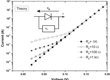
of many resistances including contribution of the substrate [57]. This latter has been estimated close to 25 Ω for a contact diameter of 2 mm. The effect of series resistance is therefore not negligible and must be taken into account. The shunt resistance is a parallel resistance to the Schottky diode which may account for leakage current. The relationship between the current I and the voltage is now given by the following equation :
I = IS(e
q(V −IRS )
nkT −1) + V − IRS RP
(2.14) As RP is parallel to the Schottky diode, its effect decreases with the increase of the shunt resistance. Fig. 2.9shows the calculated I-V curves for different values of RP in the range 0-1 kΩ and by taking RS=0. As seen, RP only affects the I-V behavior at low voltage. However Werner [65] showed that the correction of the forward current I is not influenced by the determination of the different parameters of diodes if the Schottky barrier qφIV
B is inferior to 0.83 eV. As the Schottky barrier height determined from I-V curves does not exceed 0.55 eV in this study, the effect of RP has been neglected.
Figure 2.9: Comparison of the forward I-V characteristics from Eq. 2.14 with different shunt
The relationship between the current and the voltage is then given by:
I = IS(e
q(V −IRS )
nkT −1) (2.15)
Fig. 2.10 shows the calculated I-V curves from Eq. 2.15. As seen on this figure, the series resistance leads to a deviation from linearity at higher voltage than the shunt resistance. As the effect of RS increases with the current, the deviation from linearity occurs at lower voltage with the temperature.
Figure 2.10: Comparison of forward I-V characteristics from Eq. 2.15 for different series resistance
by using the following parameters: RP = 0 Ω, Is=10−6 A, n= 1, T=130 K.
If the Schottky contact is weakly resistive, the parameters n and IS should be determined firstly from the linear region of the I-V curve and thereafter the series resistance is given by fitting the experimental curve with Eq. 2.15.
If the Schottky contact is highly resistive, the determination of the diode parameters is more problematic as the plot ln I = f(V ) shows no linear region. Several methods are proposed to determine the series resistance [65–67]. These methods often use the plot of auxiliary functions. A comparison of these methods is detailed in [63]. In particular, a method has been developed by Werner to extract the electrical parameters of highly resistive diodes [65]. However in this work, we have limited our study in a temperature range 80-230K where the diode parameters can be extracted from the linear region without needing the knowledge of RS (see Chapter 3).
2.3.4
Extraction of SBH from C-V or I-V characteristics ?
As it has been described previously, the Schottky barrier height can be determined by either C-V characteristics (φCV
B ) or I-V characteristics (φIVB ). For an ideal Schottky diode, the rela-tion φCV
Any damage at the interface affects the I-V behavior because defects may act as recombination centers or as intermediate states for trap-assisted tunnelling currents, modifying thus the SBH extracted from the I-V measurement.
The sequence φCV
B > φIVB has been observed for a large variety of metals deposited on semicon-ductors [68]. To explain this behavior, a first model has been proposed in 1979 by Ohdomari et al. [69]. These authors explained the difference between φCVB and φIVB by assuming the presence of two Schottky diodes with different SBH connected in parallel. Indeed, in this case, the lower barrier height dominates the I-V behavior, whereas the C-V characteristics are dominated by the largest contact area.
To overcome the limitation due to two different and discrete values of Schottky barrier heights, another model has been proposed by J.H Werner and H.H Güttler in 1991 [70]. This model assumes a continuous Gaussian distribution of the Schottky barrier heights across the contact. According to the authors, this model is more accurate to describe the spatial fluctuation of SBH arising from roughness of the interface, grain boundaries and different metal phases in contact with the semiconductor.
2.3.5
I-V reverse characteristics
According to the thermionic-emission theory, the reverse current of an ideal Schottky diode should saturate at the value IS = AA∗T2e
−qφIV
B
kT [62]. However, the application of an electric field causes the image-force induced lowering of the potential energy for charge carrier emission. Considering an electron, in vacuum, at a distance x from a metal surface, a positive charge will be induced on the metal at a distance -x from its surface and will give rise to an attractive force between the two, known as the image force. This force has associated with it an image potential energy which corresponds to the potential energy of an electron at a distance x from the metal. When an external field, Eext, is applied, together with these two energy components, have the effect of lowering the Schottky barrier. Thus at high fields, the Schottky barrier is considerably lowered. For a metal/semiconductor junction, the field is now replaced by the maximum field, Emax. The amount of reduction due to the induced-image-force, ∆φimage is given by:
∆φimage = 2xmEmax = { q3N D 8π2εε3 0 (φIV B − VR−(EC − EF) − kT q )} 1 4 (2.16) where
Emax = 2qND εS s φB− V − kT q ln NC ND − kT q (2.17)
If the absence of true saturation (soft reverse characteristic) is often ascribed to the image force lowering, its effect has been found to be insufficient to fully account for the soft nature of the reverse characteristic (in metal-silicide Schottky diodes for example). A further correction has been proposed by Andrews and Lepselter to bring theory into agreement with experiment [71]. This later static correction is attributed to a dipole layer at the metal/semiconductor interface caused by a charge distribution associated with surface states or to a layer of oxide or contamination between the metal and the semiconductor. This dipolar barrier lowering effect is approximated by a single term, adjustable empirical parameter α, linear in electric field. Changes in SBH are approximated by:
φIVB (V ) = φIVB0−∆φimage− αEmax (2.18)
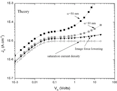
The effects of these two mechanisms are presented on Fig. 2.11for different values of α and by using the parameter of the Germanium devices (ND = 1014 cm−3, qφB= 0.43 eV, Vbi=0.37 V, T=190 K).
Figure 2.11: : Reverse characteristics at 190K (density of current vs reverse voltage) from Eq. 2.18,
by taking into account corrections on the SBH under voltage.
2.3.6
Deep-Level Transient Spectroscopy (DLTS)
DLTS (Deep Level Transient Spectroscopy), first proposed by Lang [72] is a capacitance mea-surement technique spectroscopic in nature that it can resolve peaks attributable to different electrically active traps present in the space charge region of a semiconductor. The presence of each trap is indicated by a peak on a flat baseline reflecting a measured change of capacitance along a temperature scale. The peak height is proportional to the trap concentration and the sign of each peak, positive or negative, indicates the nature of the trap (majority or minority carrier trap).
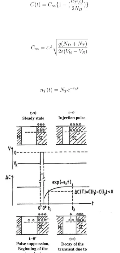
The thickness of the SCR can be modified by applying a positive voltage pulse when the Schottky diode is under a reverse voltage. This short pulse (5 ms in this study) enables the deep level traps present in the SCR to capture carriers that will thereafter be emitted, thus leading to a variation of the Schottky diode capacitance with the time called capacitive transient as illustrated in Fig. 2.12.
If the concentration of deep-levels is greatly inferior to the doping concentration (NT/ND < 10%), the capacitance, C(t), can be approximated to :
C(t) = C∞{1 − ( nT(t) 2ND )} (2.19) With: C∞= εA v u u t q(ND+ NT) 2ε(Vbi− VR) (2.20) And: nT(t) = NTe−ent (2.21)
Figure 2.12: Change of the capacitance under the influence of an applied voltage as a function of
Where ε is the permittivity of the material, A the area of the contact, ND the donor concen-tration, Vbi the built-in potential, VR the reverse bias voltage, NT the total trap concentration and en the emission rate of the defect. For the simple case of point defects, the emission rate en (i.e. the probability to emit one electron per unit time) is given by:
en(T ) = σnνthNCe
−(EC −ET )
kT (2.22)
with νththe thermal velocity of electrons, NC the density of state in the conduction band, EC is the edge conduction band energy, ET the deep level energy and σn the capture cross section. These last two constitute the signature of the deep-level traps. The change in capacitance is thus: C(t) − C∞ C∞ = NT(t) 2ND (2.23)
The apparatus (BioRad DL8000) used in this study is a digital DLTS system based on Fourier analysis of transients collected as a function of temperature. For each measured tran-sient, the software calculates 18 different signals composed in particular of the first and second order Fourier coefficients with different rate window and of rectangular functions. Each of the above signals will contribute to a point of the Arrhenius plot. Some of the weighting functions often used are shown in Fig. 2.13. Since the different weighting functions emphasize a slightly different part of the transient, it is possible to resolve closely spaced deep levels.
Figure 2.13: Typical weighting functions used by the DL8000 software. The most common weighting
function used in the following spectra will be the sine function: b1 = sin(2πT ).
2.4
Application of DLTS to the Ni/n-Ge contact
To valid (and to test) our experimental procedure, nickel germanide Schottky barriers have been first prepared on pre-treated n-type germanium. Before deposition of 30 nm of Ni by EBD, the n-type Ge substrates have been pre-treated at 700°C. One of the sample has then been submitted to post-deposition annealing (700°C, 40’+20’ ramp). The Ni/Ge contacts have been then evaluated by DLTS and the results have been compared with previous results which have shown the Ni in-diffusion during germanidation [40, 53].
Figure 2.14: DLTS spectra normalized
by the amplitude of the Ni/Ge samples before (Ni/Ge P700 ) and after (Ni/Ge
P700A) post-metal annealing with the
following parameters: VR= −4 V, VP = −0.1 V, tP = 5 ms, tW = 51.2 ms.
Figure 2.15: Arrhenius plots of the
three DLTS lines observed in Fig. 2.14.
Fig. 2.14 shows the DLTS spectra obtained before (sample named Ni/Ge P700 ) and after post-deposition annealing (700°C, sample named Ni/Ge P700A). Onto both samples, 30 nm of Ni have been evaporated (see Chapter 2.1). Spectra have been normalized by the amplitude to compare them. One level is clearly resolved before annealing whereas after annealing another peak appears at lower temperature. These two clearly defined traps, labeled E158 and E175,
have energies of EC−0.31 eV and EC−0.36 eV, respectively and apparent capture cross section of 5 × 10⁻¹⁵ cm2 and 1 × 10⁻¹⁴ cm2 (see Tab. 2.3). These signatures have been derived from
Arrhenius analyses (see Fig. 2.15).
Sample Trap EC − ET (eV ) σa (cm2) NT (cm−3) r Identification Ni/Ge P700 E175 0.36 1.0 × 10⁻¹⁴ 7.6 × 10¹² 0,9965 Cu 2−/3− S Ni/Ge P700A E158 0.31 5.4 × 10⁻¹⁵ 2.4 × 10¹¹ 0,9872 N i −/2− S E175 0.34 3.9 × 10⁻¹⁵ 2.6 × 10¹¹ 0,9910 Cu 2−/3− S
Table 2.3: Energy, apparent capture cross-section, concentration and coefficient of regression of the
By comparing with the literature, the energy and the apparent capture cross section of the deep level E158 are in good agreement with previous DLTS results for the NiS double acceptor level: Ni−/2−
S (EC − ET=0.30 eV and σa = 1.8 × 10⁻¹⁵ cm2 in [40]). E175 has been assigned to
the Cu2−/3−
S level by comparing with the literature. Indeed, copper is a common contaminant of germanium and its presence has been reported in previous studies [38,39]. The origin of this contamination will be discussed in Chapter 3.
Theses preliminary experiments conducted on the Ni/Ge system led to the following con-clusion: the e-beam deposition and the thermal pre-treatment are techniques that can be both used to elaborate Schottky contacts onto Ge and to study the diffusion of metallic species.
As-deposited samples : electrical
properties and microstructure
The influence of surface pre-treatments (HF etching, thermal annealing) on the electrical char-acteristics of Co/n-Ge Schottky diodes elaborated by EBD has been studied through the com-bination of TEM observations and electrical measurements. Different results were expected, especially due to the possible influence of the pre-treatments on the removal of the native ger-manium oxide. In addition, DLTS experiments have been performed to detect any possible metal contamination and metal in-diffusion during the process of deposition.
3.1
Microstructural characterization: TEM analyses
3.1.1
Reference sample
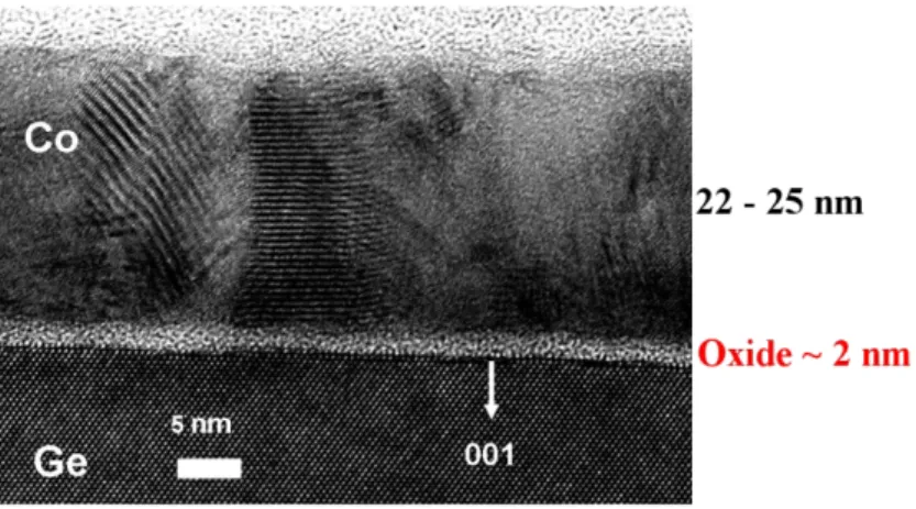
Figure 3.1: HRTEM micrograph in the cross-section geometry of the reference sample (no
pre-treatment).
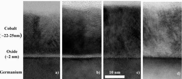
Fig. 3.1displays the HRTEM image of the reference sample (no pre-treatment) in the cross-section geometry (X-HRTEM). As seen, a two layer structure is observed after Co deposition onto the Ge substrate. A continuous layer of Co, 22-25 nm thick, is observed onto a 2 nm thick amorphous-like layer, corresponding to the native germanium oxide. The determination of the different thicknesses has been done by using the inter-reticular distance of the (001) germanium planes directly measured on the picture. The thickness of the as-deposited Co layer has been confirmed by reflectivity measurements (over a larger surface of 10−3 mm2). Moiré patterns
(intensity interferences) are observed on the Co film (Fig. 3.1) thus showing that the Co-film is polycrystalline.
Fig. 3.2 shows the selected area diffraction pattern of the reference sample. Three differ-ent rings (blues arrows on Fig.3.2) are present on the figure confirming the polycristallinity of the Co thin film. Close to the transmitted spot, the first ring, thicker than the other ones, corresponds to inter-reticular distances varying from 2.14 to 1.90 Å. The second and the third well defined rings correspond respectively to inter-reticular distances of 1.24 and 1.03 Å. The first ring is the best indicator to discriminate between the two probable cobalt crystallographic structures: the hexagonal closed-packed structure (hcp) and the body-centered cubic (bcc) structure. The two other rings are common to both structures.
Figure 3.2: Diffraction pattern of the reference sample. The simulated diffraction spots of the Ge
[110] substrate are in orange. The simulated diffraction rings of the hcp and bcc structure of Co are in green and red, respectively. The blue arrows highlight the experimental rings corresponding to the Co thin film.
The diffraction rings have thus also been simulated by using the Electron Diffraction soft-ware for the hcp and bcc phases and plotted onto the experimental diffraction pattern (see green rings and red rings of Fig. 3.2). Concerning the first rings, the hcp phase presents three rings close to each other with the following inter-reticular distances : 2.17, 2.04 and 1.94 Å ascribed, respectively, to the (010), (002) and (011) planes. The simulated diffraction rings of the bcc phase present two rings closed to the transmitted spot with the following inter-reticular distances : 2.06 and 1.78 Å corresponding, respectively, to the (111) and the (002) planes (red rings on Fig.3.2). As seen, the best match between the experimental and simulated diffraction patterns is thus obtained for the hcp structure.
In addition, Fig. 3.3 shows a profile of the intensity around the first ring. As can be seen, three peaks are clearly identified corresponding to the following inter-reticular distances : 2.14, 2.01 and 1.90 Å. These three distances agree well, within the experimental errors, with the first expected inter-reticular distances of the hcp phase. This is consistent with the expected structure in normal conditions of pressure and temperature; the allotropic transformation from
Figure 3.3: Profile of intensities from the diffraction pattern of Fig. 3.2. The measured inter-reticular
distances of the first ring are given and have to be compared with the following inter-reticular distances of the hcp structure : 2.17, 2.04 and 1.94 Å corresponding to the (010), (002) and (011) planes. the hcp Cobalt to bcc occurring at 400°C [73].
3.1.2
Pre-treated samples
Figure 3.4: TEM bright-field micrographs of the Co thin films on Ge substrate deposited by e-beam
evaporation. a) REF b) P 400 c) P 700 d) P HF .
Fig. 3.4displays X-HRTEM micrographs of the four studied samples after cobalt deposition. Between the cobalt layer and the germanium substrate, a thin amorphous-like layer, 2 nm thick, has been observed in both the reference sample (REF ) and the sample pre-treated at 400°C (P 400). No evidence of this amorphous layer has been seen on samples pre-treated at 700°C (P 700) nor by HF (P HF ). These observations show that a threshold temperature Ts, 400°C<Ts<700°C, exists, above which the native oxide can be removed under annealing in high
vacuum. This temperature is, however, strongly dependent on the atmosphere; indeed Zhou et al. [74] have observed the reduction of GeOx under wet-N2 ambient for a given temperature
and Dimoulas et al. have observed the desorption of the native germanium oxide by heating the substrate at 360°C during 15’ in UHV [31]. Moreover, the structure of the Co films is not dependent on the cleaning procedure: all the films are polycrystalline with nanometer sized grains of hcp structure for the studied four samples. The cleaning procedure has thus no effect on the microstructure of the Co film but has a strong influence on the presence or not of an oxide interfacial layer.
3.2
Electrical characterization: general considerations
3.2.1
C-V and I-V forward measurements at a fixed temperature:
160 K
As the intrinsic carrier concentration (ni) of germanium is equal to 1013cm−3 at room temper-ature, our lowly doped samples have been studied at a given temperature of 160K to minimize the thermal generation of carriers (ni/ND = 10−4, EC− EF=0.15 eV).
Figure 3.5: Reverse and forward I-V
plots at 160 K for the as-deposited sam-ples.
Figure 3.6: Experimental and fitting curves
using the thermionic model (TE) of the I-V forward characteristics at 160 K.
Fig. 3.5 shows typical semi-logarithmic I-V plots of electron beam as-deposited samples at 160K. Whatever the pre-treatment a good quality rectifying Schottky barrier, indicated by the linearity of the lnI as function of V plot in the low voltage regime (V < 0.2V ), has been
![Figure 1.7: Schematics of the band diagram of a) a strongly pinned Schottky contact and b) a pinning-alleviated contact by insertion of a thin tunneling oxide, taken from [28].](https://thumb-eu.123doks.com/thumbv2/123doknet/7969796.267051/17.892.149.704.622.888/figure-schematics-diagram-strongly-schottky-alleviated-insertion-tunneling.webp)
![Figure 2.3: Principle diagram of electron beam deposition, taken from [55].](https://thumb-eu.123doks.com/thumbv2/123doknet/7969796.267051/25.892.281.572.197.521/figure-principle-diagram-electron-beam-deposition-taken.webp)
![Figure 3.2: Diffraction pattern of the reference sample. The simulated diffraction spots of the Ge [110] substrate are in orange](https://thumb-eu.123doks.com/thumbv2/123doknet/7969796.267051/47.892.215.641.197.613/figure-diffraction-pattern-reference-sample-simulated-diffraction-substrate.webp)