HAL Id: hal-00720082
https://hal.archives-ouvertes.fr/hal-00720082
Submitted on 23 Jul 2012
HAL is a multi-disciplinary open access
archive for the deposit and dissemination of sci-entific research documents, whether they are pub-lished or not. The documents may come from teaching and research institutions in France or abroad, or from public or private research centers.
L’archive ouverte pluridisciplinaire HAL, est destinée au dépôt et à la diffusion de documents scientifiques de niveau recherche, publiés ou non, émanant des établissements d’enseignement et de recherche français ou étrangers, des laboratoires publics ou privés.
High-speed photodetectors in a photonic crystal
platform
Luisa Ottaviano, Elizaveta Semenova, Martin Schubert, Kresten Yvind,
Andrea Armaroli, Gaetano Bellanca, Stefano Trillo, Thanh Nam Nguyen,
Mathilde Gay, Laurent Bramerie, et al.
To cite this version:
Luisa Ottaviano, Elizaveta Semenova, Martin Schubert, Kresten Yvind, Andrea Armaroli, et al.. High-speed photodetectors in a photonic crystal platform. CLEO: Science and Innovations, May 2012, San Jose, United States. pp.CM1A.2. �hal-00720082�
High-speed photodetectors in a photonic crystal platform
Luisa Ottaviano1, Elizaveta Semenova1, Martin Schubert1, Kresten Yvind1 Andrea Armaroli2, Gaetano Bellanca2, Stefano Trillo2
Thanh Nam Nguyen 3,4, Mathilde Gay3,4, Laurent Bramerie3,4, Jean-Claude Simon3,4 (1) DTU Fotonik, Department of Photonics Engineering, Technical University of Denmark, 2800 Kgs.Lyngby, Denmark
(2) Optics & Photonics Group, University of Ferrara, Engineering Department, 44122 Ferrara, Italy (3)Universite Europeenne de Bretagne (UEB), 5 Boulevard Laënnec, 35000 Rennes, France (4) CNRS-Foton Laboratory (UMR 6082), Enssat, BP 80518, 22305 Lannion Cedex, France
luot@fotonik.dtu.dk
Abstract: We demonstrate a fast photodetector (f3dB > 40GHz) integrated into a high-index contrast photonic crystal platform. Device design, fabrication and characterization are presented.
OCIS codes: (040.5160) Photodetectors, (050.5298) Photonic crystals, (130.3120) Integrated optics devices
1. Introduction
High index contrast integrated optics like photonic crystals allow very small high-Q cavities for optical filtering [1] and high Q/V cavities for efficient light-matter interaction for e.g. all-optical switching [2]. It is therefore attractive for high-density photonic integration. Besides the efficient passive functionalities, sources and detectors are needed for full functionality of these integration platforms [3]. In this paper we make the first demonstration of a new high-speed photodetector concept integrated into a single-mode photonic crystal platform.
2. Photodetector fabrication
In this section we describe the fabrication of photodetectors compatible with the photonic crystals technology. The photodetector is built as a vertical pin structure integrated with a photonic crystal (PhC) waveguide (WG), i.e. an InGaAsP (PQ(1.15)) layer which extends to the rest of the wafer and allow functional photonic crystal and wire waveguides. The design is shown in Figure 1a) and c) where a PhC WG is suitably widened to optimize optical transmission and a tapered detector is inserted in it. However, the developed process is quite versatile and can be used for many different designs.
In the first step of the process flow the n-doped semiconductor is patterned by photolithography. This is followed by electron beam lithography (EBL) to define the WG. Hydrogen silsesquioxane (HSQ), a negative tone resist that works directly as a hard mask, is used for the (EBL). Then BCB polymer is used in order to planarize the wafer before n-contact metallization. The wafer is now bonded to a silicon carrier wafer using BCB and the substrate is removed. In the following step the photodetector area is defined using e-beam lithography and the mesa is defined using first dry and subsequently wet etching leaving the PQ(1.15). Again BCB is used to planarize the sample before the p-contact metallization. The final result is seen in Figure 1b). Figure 1c) shows a cross sectional view of the photodetector at the black line in Figure. 1a).
PD n side p contact n contact WG c) a) PD p-side PQ(1.15) InP:Si InGaAs PQ(1.25):Zn Pd/Au Ti/Au Si SiO2 BCB c) d) b)
Figure 1: a) Mask design for the photodetector fabrication. b) Optical microscopy of fabricated device. c) Cross section schematic detector structure. d) Small signal response measurements on a photodetector performed at 5 different bias levels. S21 is related to the electrical signal and
One important result from TLM structures on these wafers is that the resistance of the n-layer (200nm doped 1*1018cm-3) is not significantly influenced by the presence of holes. Earlier results at lower doping densities show a strong impact of the photonic crystal holes [4], but it seems that for the higher doping densities, the surface states are not able to deplete the layers.
3. Device characterisation
Small signal dynamic measurements in the range 0 – 40GHz have been performed in order to evaluate the photodetector bandwidth. A Network analyzer calibrated with a u2t 50GHz photodiode has been used for this purpose; the 2dB drop at 40GHz of the u2t diode has not been taken into account in the calibration. The measurements have been performed with a 50GHz GSG (ground-signal-ground) probe from Picoprobe®. As it is possible to see from the S21 curves shown in Figure 1d), the photodetector has a 3dB bandwidth bigger than 40GHz at -2V.
4. System characterisations
System assessment was performed at CNRS FOTON with a Non-Return-to-Zero signal at 1310nm. The signal, encoded with a 231-1 pseudo random bit sequence at 10 and 20Gbit/s through a Mach Zenhder modulator, was amplified through a Semiconductor Optical Amplifier for an input power varying between 3 and 10dBm on direct detection. No electrical amplification was used for additional thermal noise limitation and receiver sensitivity improvement. A polarisation controller allowed selecting the proper polarisation state in the PhC WG. The bias voltage of the photodetector was set at -2.5V.
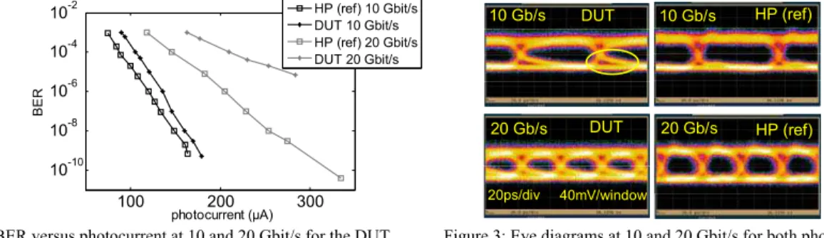
The Bit Error Rate (BER) was measured as a function of photocurrent at 10 and 20Gbit/s. The photodetector under test (DUT) was compared to a commercial InGaAs PIN photodetector with a 3dB bandwidth of 32GHz (HP 83440D). We observed error free operation at 10Gbit/s and a similar behaviour for our photodetector in comparison to the reference (less than 10µA penalties at 10-9). However at 20Gbit/s our photodetector exhibited some penalties (100µA penalties at 5.10-6), see Figure 2. Eye diagrams at 10 and 20Gbit/s are presented in Figure 3 for a fixed photocurrent of 170µA. The similar amplitude of the eye diagrams at both bit rates and the steep flanks of the eye diagram show that photodetector bandwidth must not be at the origin of the degradation. The eye diagram deformation on low level (yellow circle in the figure) is probably at the origin of penalties; we believe that this deformation is due to an impedance mismatch which is not adjusted at this stage.
10 Gb/s 20 Gb/s 40mV/window 20ps/div DUT HP (ref) DUT 20 Gb/s HP (ref) 10 Gb/s 10 Gb/s 20 Gb/s 40mV/window 20ps/div DUT HP (ref) DUT 20 Gb/s HP (ref) 10 Gb/s 100 200 300 10-10 10-8 10-6 10-4 10-2 photocurrent (µA) BER HP (ref) 10 Gbit/s DUT 10 Gbit/s HP (ref) 20 Gbit/s DUT 20 Gbit/s
Figure 2: BER versus photocurrent at 10 and 20 Gbit/s for the DUT and the reference photodiode.
Figure 3: Eye diagrams at 10 and 20 Gbit/s for both photodiodes.
4. Conclusions
A high-speed photodetector compatible with a high index contrast photonic crystal platform has been demonstrated for the first time. Error free operation was obtained at 10Gbit/s. Impedance mismatch makes higher bit rate operation difficult and we will look further on into it.
5. Acknowledgement
We acknowledge the support by the European Union, FP7/ICT funding programme, under the Copernicus project (249012) (www.copernicusproject.eu) and the VKR center of Excellence NATEC.
6. References
[1] A. Shinya et al, Ultrasmall multi-port channel drop filter in two-dimensional photonic crystal on silicon-on-insulator substrate, Opt. Ex.14, 12394 (2006)
[2] C. Husko, et al, Ultrafast all-optical modulation in GaAs photonic crystal cavities, Appl. Phy. Lett. 94, 021111 (2009)
[3]E. Viasnoff-Schwoob et al, Compact wavelength monitoring by lateral outcoupling in wedged photonic crystal multimode waveguides, Appl. Phys. Lett. 86, 101107 (2005)