HAL Id: hal-02472340
https://hal.archives-ouvertes.fr/hal-02472340
Submitted on 10 Feb 2020
HAL is a multi-disciplinary open access
archive for the deposit and dissemination of
sci-entific research documents, whether they are
pub-lished or not. The documents may come from
teaching and research institutions in France or
abroad, or from public or private research centers.
L’archive ouverte pluridisciplinaire HAL, est
destinée au dépôt et à la diffusion de documents
scientifiques de niveau recherche, publiés ou non,
émanant des établissements d’enseignement et de
recherche français ou étrangers, des laboratoires
publics ou privés.
Silicon-on-Insulator photonic crystal multi-tap
microwave photonics filter
Jérôme Bourderionnet, Gregory Moille, Sylvain Combrié, Alfredo de Rossi,
Xavier Checoury, Zheng Han, Mathilde Gay, Laurent Bramerie, Jean-Claude
Simon, Christophe Peucheret
To cite this version:
Jérôme Bourderionnet, Gregory Moille, Sylvain Combrié, Alfredo de Rossi, Xavier Checoury, et
al.. Silicon-on-Insulator photonic crystal multi-tap microwave photonics filter. 2016 IEEE
Photon-ics Conference (IPC 2016), Oct 2016, Waikoloa, Hawaii, United States. pp.281-282,
�10.1109/IP-Con.2016.7831097�. �hal-02472340�
Silicon-on-Insulator photonic crystal multi-tap
microwave photonics filter
Jérôme Bourderionnet, Grégory Moille
a, Sylvain
Combrié, Alfredo De Rossi
Thales Research and Technology
1 av. Augustin Fresnel, 91767 Palaiseau, FRANCE
Xavier Chécoury, Zheng Han
bInstitut d’Electronique Fondamentale, Univ. Paris-Saclay Orsay, FRANCE
Mathilde Gay, Laurent Bramerie, Jean-Claude Simon,
Christophe Peucheret
Foton Laboratory, CNRS, University of Rennes 1 Lannion, FRANCE
a G. Moille is now with IEF, Orsay, France b Z. Han is now with MirSense, Palaiseau, France
Abstract—We present a fully CMOS compatible frequency
shifter device, in a I&Q dual Mach-Zehnder architecture. Frequency shift up to 410 MHz are obtained, with carrier and image sideband extinction from 27 to 51 dB.
I. INTRODUCTION
Microwave photonic filters are an emerging technology for digital, radio, and space communications as well as radars. Processing signals in the optical domain can provide spectral agility, broadband operation and dynamical reconfigurability [1]. In discrete-time signal processing architectures, delayed and weighted replicas of a signal are summed, with the weighting coefficients corresponding to a given finite impulse response of the system. In photonics implementation of these tapped delay lines, an incoherent summation of the replicas is usually preferred, to get rid of optical phase instabilities between the taps. This however restricts the system to positive weighting coefficients, which can consequently only operate as a low-pass filter. In the incoherent summation regime, the optical phase between the taps has no effect on the tap weights, and the phase of the RF signal has to be manipulated to generate the negative
coefficients [2,3].
Photonic integrated circuits (PIC) technology allows the monolithic integration of a broad range of optical and RF functions on a very small footprint. Novel microwave photonics filter concept can therefore be envisaged, where the optical stability of the PIC makes possible the exploitation of the optical phase in coherent summation schemes to generate the negative weighting coefficients.
In this paper, we present the design and fabrication of a 4-taps coherent finite impulse filter device, where the optical phase is used to generate the tap coefficients. The device includes photonic crystal building blocks, to provide tunable amplitude, phase and delay in each tap. The optical phase experimental measurement and locking scheme is reported for the 2-taps unit cell.
II. DEVICE ARCHITECTURE AND FABRICATION
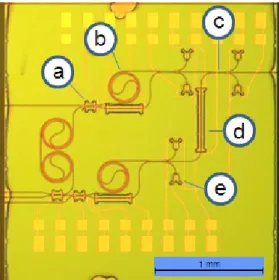
The device architecture can be seen on the picture of Fig. 1. The filter is organized in two 2-taps unitary cells (“level 0”) nested into a larger interferometer structure (“level 1”). The level 0 cells comprise a ~25ps fixed spiral delay line on one arm (labelled (b) on the picture), and a 250 µm-long tunable photonic crystal delay line on the other arm. The level 1 cell then incorporates one level 0 cell on each arm, plus 2 cascaded 25 ps spiral delay lines on one arm, and one 500 µm-long tunable photonic crystal delay line on the other arm (labelled (d) on the picture). Fig. 3a shows a SEM image of the suspended membrane photonic crystal delay line, which consists in a slow-light waveguide, whose group index is changed by locally heating the silicon membrane. For the 500 µm-long device, up to 70 ps delay excursion is achieved for 80 mW of applied electric power [4]. Owing to the extremely small volume of heated matter, the heating and cooling time of the structure is ~1µs. A low speed phase modulation can then be applied, and used for optical phase measurement and
This work was supported in part by the French National Research Agency (ANR) under the SYMPHONIE (ANR-2012-NANO-0011-01) project and by the RENATECH network.
Fig. 1. Picture of the Silicon-on-insulator 4 taps device. (a) thermally tunable photonic crystal directional coupler; (b) spiral delay line; (c) 2x3 multimode interferometer coupler; (d) thermally tunable photonic crystal delay line; (e) metal-semiconductor-metal silicon photodiodes.
Fig. 2. Schematic of the cross-section of the technological process developped at IEF. The silicon circuit is buried into a SiO2 layer, which is locally opened to allow the underetch of the photonic crystal structures.
stabilization by lock-in technique.
Each of the cells is opened by a photonic crystal thermally tunable directional coupler [5] (labelled (a)), which allows to distribute the optical amplitude between the taps. The cells are then closed by a 2x3 multimode interferometer (MMI) coupler. The central output of this MMI continues the optical circuits. The other 2 optical outputs feed on-chip photodiodes, as shown on Fig. 3(c). These photodiodes exploit exalted 2 photon absorption in a silicon slowlight waveguide [6], and exhibit an efficiency of ~0.1 A/W. The structures were fabricated in the IEF clean room. The schematic of the process cross-section is shown on Fig. 2. Once the shallow and deep etched structures have been processed by e-beam lithography, a first metal layer is deposited, and covered by a 2 µm thick silica cladding layer. This layer is locally opened for photonic crystal membrane releasing, and a second metallic layer is deposited for contact routing to bond pads. Finally, the chip is glued onto a ceramic interface and contacts are wire-bonded to the ceramic pads.
III. UNITARY CELL EXPERIMENTAL CHARACTERIZATION
In coherent MWP filters, the taps optical phase distribution is used to program the filter weights. This section details the optical phase stabilization scheme that was implemented on a
unit cell with 125ps instead of 25ps spiral delay line, using the 2 complementary outputs of the 2x3 MMI combiners for optical phase measurement. These outputs are respectively phase shifted by ⁄ with respect to the main output [7]. A weak 30 kHz sine voltage offset is applied to the photonic crystal delay line, producing 2 intensity modulated signals at the photodiodes, shifted by ⁄ radians. The demodulated signals are respectively proportional to ( ⁄ ) and ( ⁄ ) which enable a direct computation of the phase difference between the interferometer taps. A phase stabilization loop was then implemented, using an Arduino Due microcontroller. In the close loop configuration, a phase locking stability of /80 rms is achieved, as shown on Fig. 4(c). The unitary cell was inserted into a MZM-based MWP link, and the device RF transfer function was measured using a network analyzer. In Fig.4(a), a coarse tuning of the photonic crystal delay line varies the filter free spectral range from 8.7 to 9.3 GHz. The directional coupler is tuned to balance the tap amplitude, leading to an extinction ratio of -40 to -50 dB. Fig.4(b) illustrates the fine tuning the photonic crystal delay line, which enables, with our phase lock loop system, to control the optical phase between the taps. As expected for a 2 tap cell, the RF transfer function is attenuated by the sine of the optical phase shift. For larger number of taps, this will enable to produce the filter bipolar weighting coefficients.
IV. CONCLUSION
A coherent 2 tap filter unit cell is reported, which enables both tap-delay tunability and optical phase control. Monitoring photodiodes and 2x3 MMI coupler architecture enable on-chip optical phase measurement. A phase lock loop is implemented using an Arduino controller. These results validate the coherent unit-cell operation and electronic implementation, and assess the SOI technology maturity. This opens the way to structures with larger number of taps. A 4-taps filter has been fabricated and is currently under characterization.
REFERENCES
[1] [J. Capmany, B. Ortega, and D. Pastor, J. Lightw. Technol., vol. 24, no. 1, pp. 201-229, 2006.
[2] J. Capmany, et al. Opt. Lett., vol. 28, no. 16, pp. 1415–1417, 2003. [3] E. J. Norberg, et al. J. Lightw. Technol., vol. 29, no. 11, pp. 1611–1619,
2011.
[4] J. Bourderionnet, et al. European Conference on Lasers and Electro-Optics, Germany, 2015, paper CK7.3.
[5] Z. Han, et al. Opt. Express, vol. 23, no. 19, pp. 24163-24170, 2015. [6] L.-D. Haret, et al. Opt. Express, vol. 18, no. 23, pp. 23965-23972 2010. [7] T. T. Le and L. W. Cahill, Integrated Optics: Devices, Materials, and
Technologies XII. Proceedings of the SPIE, vol. 6896, pp. 68961G, 2008.
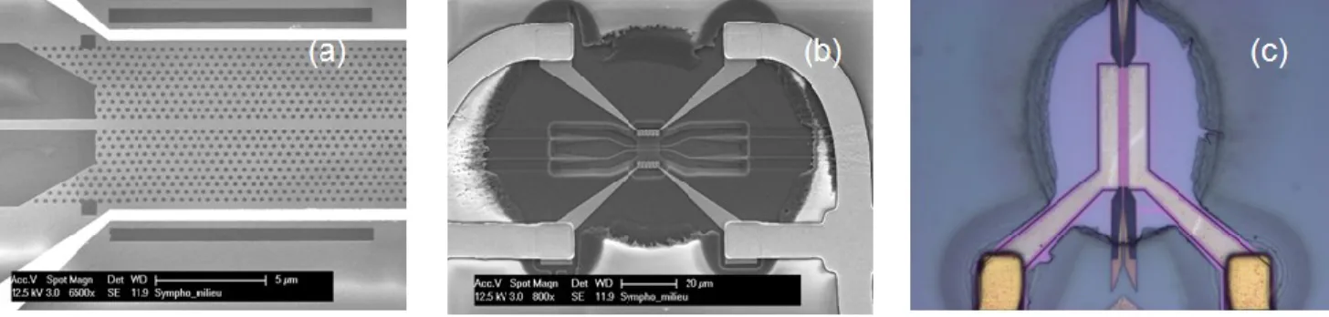
Fig. 3. (a) SEM image of the input section of the silicon suspended membrane photonic crystal delay line. Microheaters are visible on each sides of the structure. (b) Photonic crystal directional coupler, and illustration of the cladding oxyde reopening for photonic crystal underetch. (c) Metal-Semiconductor-Metal silicon photodiode.
Fig. 4. Experimental measurements of the unitary cell RF transfer function. (a) Coarse tuning of the PhC delay line varies the tap delay: the filter free spectral range is tuned from 8.7 to 9.3 GHz. (b) Fine tuning of the PhC delay line varies the tap optical phase shift , which uniformly attenuates the transfer function by sin(). (c) Time trace of the residual phase error when the phase lock loop is closed.