Any correspondence concerning this service should be sent to the repository administrator:
[email protected]
O
pen
A
rchive
T
oulouse
A
rchive
O
uverte (
OATAO
)
OATAO is an open access repository that collects the work of Toulouse researchers
and makes it freely available over the web where possible.
This is an author - deposited version published in:
http://oatao.univ-toulouse.fr/
Eprints ID: 4839
To link to this article: DOI: 10.1109/LED.2011.2127442
URL:
http://dx.doi.org/10.1109/LED.2011.2127442
To cite this version: MARTIN-GONTHIER Philippe, MAGNAN Pierre. Novel readout
circuit architecture for CMOS image sensors minimizing RTS noise. IEEE Electron Device
Letters, vol. 32, n° 6, pp. 776 -778.
Novel Readout Circuit Architecture for CMOS
Image Sensors Minimizing RTS Noise
Philippe Martin-Gonthier and Pierre Magnan, Member, IEEE
Abstract—This letter presents a novel readout architecture and its associated readout sequence for complementary metal–oxide– semiconductor (CMOS) image sensors (CISs) based on switch biasing techniques in order to reduce noisy pixel numbers induced by in-pixel source-follower transistor random telegraph signal noise. Measurement results done on a test image sensor designed with 0.35-μm CIS technology demonstrate an efficient reduction of noisy pixel numbers without a pixel performance decrease.
Index Terms—CMOS image sensor (CIS), correlated double sampling (CDS), low frequency noise (LFN), noisy pixel reduction, random telegraph signal (RTS) noise.
I. INTRODUCTION
C
OMPLEMENTARY metal–oxide–semiconductor (CMOS) image sensors (CISs) are nowadays extensively used in commercial and scientific applications due to CIS processes [1]. In order to maximize pixel photosensitive area, the use of aggressive technologies and small in-pixel MOS transistors are required. This leads to an increase in the impact of MOS-transistor low frequency noise (LFN). The use of correlated double-sampling (CDS) circuits and a readout mode allows the elimination of photodiode reset noise (i.e., kT /C noise), which is usually a major noise contributor. At the same time, it reveals the impact of random telegraph signal (RTS) noise of an in-pixel source-follower (SF) transistor [2]. This RTS noise becomes an issue for low light sensitivity applications [3].Interface and near oxide traps in small-gate-area MOS tran-sistors (< 1 μm2) induce RTS noise when the transistor is in inversion mode. In this case, the transistor channel is in contact with gate and isolation oxides. Electrons can be captured and released depending on the trap features inducing RTS fluctua-tions of drain current [4]. Several techniques are used in order to reduce the RTS noise impact of an in-pixel SF transistor. The use of an in-pixel buried-channel SF transistor can reduce drastically RTS noise [5]. Unfortunately, this buried transistor option is not available for all CIS processes. In-pixel SF tran-sistor dimensions can be optimized to reduce RTS noise. The
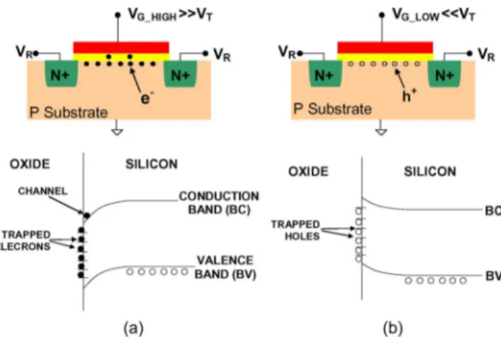
Fig. 1. Principle of the switch biasing technique. (a) nMOS in the inversion operation. (b) nMOS in the accumulation operation.
increase in transistor length and width raises Si/SiO2interface
trap numbers leading to 1/f noise instead of RTS noise [6]. This technique implies pixel conversion gain reduction due to an in-pixel SF gate capacitance increase, which is unacceptable in a lot of applications. Another technique consists of designing custom layout transistors [7]. An in-pixel SF transistor is laid out in order to minimize the isolation oxide in contact with n-channel MOS (nMOS). This promising technique modifies transistor features inducing a new model creation.
This letter presents a novel circuit architecture and a readout sequence for CISs allowing the reduction of in-pixel SF transis-tor RTS noise based on switch biasing techniques.
II. PROPOSEDREADOUTCIRCUITARCHITECTURE
BASED ONSWITCHBIASINGTECHNIQUES
Switch biasing techniques, allowing 1/f noise reduction for MOS transistors, were introduced in the early 1990s [8].
The principle is to switch alternatively an nMOS transistor from an inversion to an accumulation mode. During the nMOS transistor inversion operation [see Fig. 1(a)], electrons from the channel are captured and released by interface traps inducing RTS or 1/f noise depending on trap numbers. The nMOS transistor accumulation operation [see Fig. 1(b)] allows filling in traps with holes. Hole capture and release times depend on trap features. If the nMOS transistor is in inversion mode after the accumulation operation, traps are filled by holes, and no electrons can be captured during that time depending on the trap features. This leads to an LFN reduction. A 1/f power spectral density reduction of 6 dB can be reached [8].
MARTIN-GONTHIER AND MAGNAN: CIRCUIT ARCHITECTURE FOR CISS MINIMIZING RTS NOISE
Fig. 2. Common readout circuit architecture of a CIS.
A common CIS readout circuit architecture is shown in Fig. 2. It is composed of a photoelement, i.e., a photodiode or a pinned photodiode associated with a transfer gate; a reset switch allowing to reset the photoelement or a readout node; an in-pixel SF, which drives the signal from a pixel to a column readout circuit; a double sample-and-hold circuit for reference and an integrated signal level; and an output stage allowing to drive the signal off or on chip for additional processing.
For a three-transistor (3T) photodiode pixel, at the beginning of a line period, the photodiode is reset by a reset MOSFET (i.e., the command signal is RST). This level, which is called reference, is sampled and held (i.e., the command signal is SHR) in the column readout circuit in the reference channel via the in-pixel SF and a row selection transistor. During the integration time, the photodiode is in self-integrating mode (i.e., integrating charges in its own capacitance). At the end of the integration time, the voltage level corresponding to the integrated charges is sampled and held (i.e., command signal is SHS) in the column readout circuit of the signal channel. A video signal voltage level results from the subtraction of the two samples (i.e., the reference and the signal). In this letter, in order to study RTS noise and remove reset noise from the 3T photodiode pixel, a specific readout sequence allowing CDS is applied (see Fig. 3). This specific readout sequence allows reset noise cancelation as for the pinned photodiode (i.e., a four-transistor (4T) photodiode pixel).
A switch biasing technique was firstly implemented in a common CMOS readout circuit of a CIS allowing CDS without a specific circuit and a readout sequence [9]. In this case, the switch biasing technique was applied only before the sampling phase (i.e., composed of the two samples). Experimental results of this letter showed no RTS noise reduction. The major conclu-sion of this letter showed that switch biasing must be applied before each sample and not before the sampling phase.
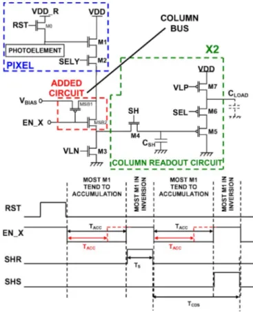
The proposed circuit architecture and its associated readout sequence, shown in Fig. 3, use the switch biasing technique before each sample without pixel performance, and the read-out frame rate decrease. This architecture is composed of
Fig. 3. Proposed circuit allowing the efficient switch biasing technique.
the common readout circuit and an added circuit, i.e., two MOS transistors inserted in the column. In standard readout mode without the added circuit, when the SELY command is enabled (i.e., set to VDD), the pixel is selected, and the M1 transistor is in inversion mode (i.e., the SF). In this mode and after the reset phase, the M1 gate voltage is VDD_R if VDD_R≤ VDD − VTHM0, where VTHM0is the M0 threshold
voltage. The M1 source voltage becomes VDD_R− VTHM1.
With the proposed readout circuit architecture and after the reset phase, the voltage bias VBIAS and the command signal
EN_X can put the in-pixel SF transistor M1 off in order to tend to the accumulation mode. Indeed, before each sample (i.e., the reference and the signal), the VBIASvoltage is applied
with the EN_X command to the column bus through MSB1. Due to the presence of M2, the M1 source voltage is VBIAS−
VTHM2. As the M1 gate voltage is still VDD_R, if VBIAS is
set to VDD, the M1 gate-to-source voltage VGS tends to 0 or
less. In this case, the M1 transistor tends to the accumulation mode before each sample. The other chronogram phases are unchanged comparing to the original sequence, and the pixel can be readout normally.
Therefore, with this added structure, during each sampling phase (i.e., when MSB1 is off and MSB2 is on), the in-pixel SF transistor stays in inversion mode, and the M1 source voltage is VM1_SOURCE= VM1_GATE− VTHM1, where
VM1_GATE is the M1 gate voltage. Before each sampling
phase (i.e., when MSB1 is on and MSB2 is off), the M1 source voltage is VM1_SOURCE= VBIAS− VTHM2, and M1
tends to the accumulation mode leading to RTS noise reduction (noisy pixels).
Fig. 4. Cumulative histogram of sensor output noise with and without the switch biasing technique for TACC= 2.15 μs, VBIAS= 3.3 V and
VDD_R = 2.5 V.
This architecture with the added circuit in the column of the image sensor and its associated readout sequence, which can also be implemented with a 4T pixel structures, have no impact on pixel fill factors, conversion gain, and output readout speed. Due to the working mode of the in-pixel SF transistor (M1) and the current source transistor (M3) during the sampling phase, M1 noise and M3 noise dominate the noise performance of this stage. Indeed, noise due to M2 and MSB2, which are considered as switches, can be neglected [10]. Therefore, the added circuit does not have an impact on the noise performance of this stage.
This circuit was implemented in a test image sensor designed with a CIS 0.35-μm technology using conventional photodiodes (3T pixels). The accumulation time TACCcan be set to several
values.
III. EXPERIMENTALRESULTS
Noise measurement procedures were done on the test image sensor. Fig. 4 shows a cumulative histogram of sensor output noise with and without the switch biasing technique applied to the in-pixel SF transistor (TACC= 2.15 μs, VBIAS= 3.3 V,
and VDD_R = 2.5 V). The cumulative histogram is the best representation to study noisy pixel numbers impacted by RTS fluctuations. These measurements show a real impact of the switch biasing technique with a decrease in noisy pixels. For example, at 200 μV (root mean square), a pixel number reduc-tion of 2 is achieved due to this architecture.
Fig. 5 illustrates the sensor output noise cumulative his-togram as a function of the accumulation time TACCof the
in-pixel SF transistor before each sample. The accumulation time decrease implies a reduction of switch biasing technique effi-ciency, which is confirmed by measurements.The measurement set on this test image sensor confirms that no impact is found on general image sensor parameters (e.g., dark current, conversion gain, and quantum efficiency).
Fig. 5. Cumulative histogram of sensor output noise as a function of the accumulation time TACCof the in-pixel SF.
IV. CONCLUSION
In this letter, a novel readout circuit architecture for CISs and its associated readout sequence have been proposed to reduce in-pixel SF transistor RTS noise inducing noisy pixels. This technique, based on switch biasing, shows an efficient decrease in noisy pixels without a pixel fill factor, conversion gain, and an output readout speed decrease.
REFERENCES
[1] M. Furumiya, H. Ohkubo, Y. Muramatsu, S. Kurosawa, F. Okamoto, Y. Fujimoto, and Y. Nakashiba, “High sensitivity and no-crosstalk pixel technology for embedded CMOS Image Sensor,” IEEE Trans. Electron
Devices, vol. 48, no. 10, pp. 2221–2227, Oct. 2001.
[2] P. Martin-Gonthier and P. Magnan, “RTS noise impact in CMOS image sensors readout circuit,” in Proc. 16th IEEE ICECS, Dec. 13–16, 2009, pp. 928–931.
[3] K. Findlater, J. M. Vaillant, D. J. Baxter, C. Augier, D. Herault, R. K. Henderson, J. E. D. Hurwitz, L. A. Grant, and J.-M. Volle, “Source follower noise limitations in CMOS active pixel Sensors,” in Proc.
SPIE—Detectors and Associated Signal Processing, 2004, vol. 5251,
pp. 187–195.
[4] M. J. Kirton and M. Uren, “Noise in solid-state microstructures: A new perspective on individual defects, interface states and low-frequency (1/f) noise,” Adv. Phys., vol. 38, no. 4, pp. 367–468, 1989.
[5] Y. Chen, X. Wang, A. Mierop, and A. Theuwissen, “A CMOS image sensor with in-pixel buried-channel source follower and optimized row selector,” IEEE Trans. Electron Devices, vol. 56, no. 11, pp. 2390–2397, Nov. 2009.
[6] A. F. Assaf Lahav and A. Shiwalkar, “Optimization of random telegraph noise non uniformity in a CMOS pixel with a pinned-photodiode,” in
Proc. Int. Image Sens. Workshop, 2007, pp. 219–223.
[7] P. Martin-Gonthier, E. Havard, and P. Magnan, “Custom transistor layout design techniques for random telegraph signal noise reduction in CMOS image sensors,” Electron. Lett., vol. 46, no. 19, pp. 1323–1324, Sep. 2010. [8] I. Bloom and Y. Nemirovsky, “1/f noise reduction of metal–oxide– semiconductor transistors by cycling from inversion to accumulation,”
Appl. Phys. Lett., vol. 58, no. 15, pp. 1664–1666, Apr. 1991.
[9] M. F. Snoeij, A. P. van der Wel, A. J. P. Theuwissen, and J. H. Huijsing, “The effect of switched-biasing on 1/f noise in CMOS imager front-ends,” in Proc. IEEE Workshop CCDs Adv. Image Sens., Karuizawa, Japan, Jun. 9–11, 2005, pp. 68–71.
[10] H. Tian, B. Fowler, and A. E. Gamal, “Analysis of temporal noise in CMOS photodiode active pixel sensor,” IEEE J. Solid-State Circuits, vol. 36, no. 1, pp. 92–101, Jan. 2001.