an author's https://oatao.univ-toulouse.fr/23023
Goiffon, Vincent and Allanche, Timothé and Muller, Cyprien and Girard, Sylvain and Paillet, Philippe and Macé, Jean Reynald and Osmond, Melanie and Burnichon, Pierre and Plumeri, Stéphane and Baudu, Jean-Pierre and Boukenter, Aziz and Magnan, Pierre and Rizzolo, Serena and Corbière, Franck and Duhamel, Olivier and Rousson, johanna and Desjonquères, Hortense and Molina, Romain and Ouerdane, Youcef and Lépine, Thierry CAMRAD: Development of a Multi-Megagray Radiation Hard CMOS Camera for Dismantling Operations. (2018) In: Dismantling Challenges: Industrial Reality, Prospects and Feedback Experience (DEM 2018), 22 October 2018 - 24 October 2018 (Avignon, France).
CAMRAD: Development of a Multi-Megagray Radiation Hard CMOS
Camera for Dismantling Operations
Vincent Goiffon1*, Timothé Allanche2, Cyprien Muller2,3 , Philippe Paillet3,
Jean-Reynald Macé4, Mélanie Osmond5, Pierre Burnichon6, Stéphane Plumeri7, Jean-Pierre Baudu6, Aziz Boukenter2, Pierre Magnan1, Serena Rizzolo1, Franck Corbière1, Olivier Duhamel3, Johanna
Rousson6, Hortense Desjonqueres5, Romain Molina1, Youcef Ouerdane2, Thierry Lépine2, Raphaël Clerc2,, Sylvain Girard2.
1
ISAE-SUPAERO, Université de Toulouse, F-31055, Toulouse, France
2
Université de Lyon, Laboratoire Hubert Curien, UMR-CNRS 5516, Saint-Etienne, France
3
CEA, DAM, DIF, F-91927 Arpajon, France
4Orano, 1 place Jean Millier – 92400 Courbevoie - France, France 5
Institut de Radioprotection et de Sûreté Nucléaire (IRSN),PSN-RES, SCA, LECEV, Gif-sur-Yvette, 91192 France
6
OPTSYS,7 rue Salvador Dali, F-42007 Saint Etienne, France
7
Andra, 1/7 rue Jean Monnet, Parc de la Croix-Blanche, F-92298 Châtenay-Malabry, France
* Main Author, E-mail: [email protected]
Abstract: The CAMRAD research and development project aims at developing a new high performance CMOS radiation hard camera technology that can withstand several MGy(SiO2)
of ionizing radiation without shielding and without significant image quality degradation. Such a technology will significantly benefit to the dismantling and decontamination industries by enabling the monitoring and inspection of radioactive areas that cannot be observed today. This paper presents the overall project as well as the results of the technology exploration phase aiming at selecting the best materials, designs and hardening techniques to reach the ambitious goal of CAMRAD.
KEYWORDS: Camera, Radiation Hard, Ionizing Radiation, Imaging System, CMOS Image Sensor, Optics, Optical System, Rad-Hard Glass, LED, Monitoring, Inspection
Introduction
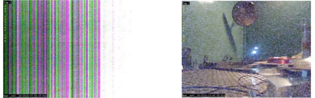
Dismantling and decontamination of shutdown nuclear facilities require the use of radiation resistant imaging systems to monitor the radioactive wastes, remote handling operations, to inspect reactors, plants or laboratories and to control dismantling robots. Tube based cameras currently offer the highest radiation hardness but they are fragile, bulky and limited in terms of performance and image resolution. Commercially available off-the-shelf (COTS) radiation tolerant camera based on solid-state image sensors, such as Charge Injection Devices (CID) or Complementary Metal Oxide Semiconductor (CMOS) Image Sensors (CIS), are limited to a maximum Total Ionizing Dose (TID) of 100 kGy(SiO2) when no shielding and no thermal annealing techniques are used to
ex-tend their lifetime (as illustrated in Figure 1).
In this work the CAMRAD research and development project is presented: it aims at developing a new high performance CMOS radiation hard camera technology that can withstand several MGy(SiO2) of ionizing
radia-tion (i.e. several hundreds of Mrad(SiO2)). CAMRAD is supported by Andra (French National Radioactive
Waste Management Agency) under the "Investing in the Future" program ("Programme d’Investissement d'Avenir (PIA)").
With its higher radiation hardness level, its lightweight and small size, such a technology could potentially change the way dismantling operations are done by allowing the inspection of radioactive areas that cannot be observed today. This technology will reduce the frequency of replacement of imaging systems and it will have a direct positive impact on costs as well as on staff safety and security in these facilities.
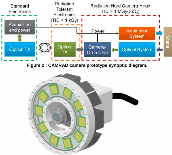
Figure 2 : CAMRAD camera prototype synoptic diagram.
Figure 3 : CAMRAD camera prototype preliminary design.
Project and Technology Overview
An overview of the CAMRAD imaging system is presented in Figure 2 and a preliminary design illustration of its camera head is displayed in Figure 3. The radiation hardened camera head includes an illumination system, an optical system and a camera-on-a-chip integrated circuit that can withstand MGy doses. To communicate with the electronic chip, especially for data transmission from the head to the acquisition computer, a radiation toler-ant electro-optical transceiver link based on a radiation hardened optical fiber is placed several meters away from the camera head. By placing the electro-optical conversion module far from radioactive area to observe, the radiation constraint is lowered down to a few kGy(SiO2). At such TID level, the electro-optical conversion
sys-tem can be designed based on existing solutions and no particular dedicated technology will be developed during the project. The selected optical fiber for this link is also considered radiation hard at this TID level [1]. Finally, the other optical transceiver and the acquisition system (left-hand side of Figure 2) are located in a radiation free zone (typically at the end of an optical link longer than 100 m) and are designed with conventional commercial electronics.
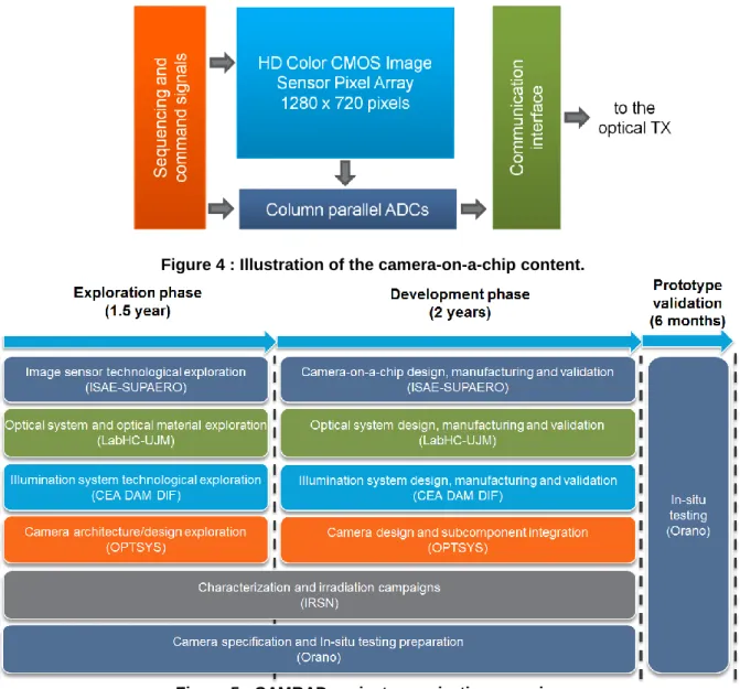
Hence, the main challenge of this project lays in the development of the Multi-MGy radiation hard camera head. The first originality of this project consists in integrating all the camera head electronics on a single chip and to harden by design the entire integrated circuit as proposed in [2], [3]. Indeed, typical radiation hardened cameras based on solid-state image sensors make use of several integrated circuits in the camera head and most of them are not hardened against MGy TID levels. The key elements integrated on the CAMRAD radiation hardened camera-on-a-chip are illustrated in Figure 4. It includes a CMOS Image Sensor and every electronic function required to operate the sensor, to digitize the pixel signal and to transmit the information to the external optical transceiver, i.e.:
a High Definition (HD) pixel array made of 1280×720 pixels with a Bayer Color Filter array (one RGB filter per pixel)
a 10-bit column parallel Analog-to-Digital Converters (ADC) an on-chip sequencer
an on-chip digital communication interface
radiation-hardening-by-design (RHBD) techniques [4], [5], especially at the device layout level. The pixel radiation-hardening-by-design itself has been treat-ed with particular attention as discusstreat-ed in [6] to meet the CAMRAD project requirements.
Figure 4 : Illustration of the camera-on-a-chip content.
Figure 5 : CAMRAD project organization overview.
The other innovation of the presented project is the development of Multi-MGy optical and illumination sys-tems as well as the parallel optimization of these three key functions in order to reach the project ambition by compensating each subsystem potential weakness by designing accordingly the other two. Such strategy explains that the Light Emitting Diode (LED) technology as well as the optical system materials have been carefully chosen to ensure the best optical budget for this image sensor technology. The nominal CMOS image sensor integration time, the LED optical power and the optical system aperture have been optimized to account for the expected radiation induced degradations or modifications of these subsystems. The exploration phase discussed hereafter is used to extrapolate the behavior of the full-size system after irradiation and to anticipate its limited radiation induced changes.
Finally, the ambition of the developed approach is also original: CAMRAD is seeking to develop a camera with a much greater resistance to ionizing radiation than existing products (cumulative dose of 1-10 MGy) with performance levels and features not generally found on this market (color image, high resolution, compact de-sign, etc.).
Existing radiation tolerant cameras are based on COTS sub-components that intrinsically limit the radiation hardness and the performance of the whole imaging system. The multi-scale radiation hardening approach start-ing from the selection of the right materials and manufacturstart-ing processes, all the way up to component radiation-hardening-by-design and system level radiation-hardening is illustrated by the project flow chart of Figure 5. Beside the overall project architecture, this figure also depicts the role of each partner and highlights their com-plementarity.
Figure 6: IRMA irradiation room Figure 7: CAMRAD contrast target, the smallest line is 1mm
To reach the goal of CAMRAD, the project has been divided into two main phases: a technological explora-tion phase (May 2016 – February 2018) and a full-scale prototype development and validaexplora-tion phase (March 2018 - May 2020). During the exploration phase, several radiation hardening strategies have been explored for each subpart of the camera. The outcomes of this first phase are detailed in the following sections.
During the second main phase, each sub-system will be developed, validated and integrated inside the camera prototype. To conclude the project, this camera prototype will be itself validated by an in-situ test that is repre-sentative of a real application case. This in-situ test will take place at the IRSN IRMA facility. The camera will record images in front of Co60 sources. Because of the size of the irradiation room of IRMA (see Figure 6) the scene will be placed at a distance of 1.5 m from the camera. This test has two main goals:
to demonstrate that the assembled camera can operate and keep the image quality during the irradia-tion up to 1 MGy
to study online radiation effects on each subsystem
This in-situ test will enable the study of online radiation effects on a CIS to such a high TID (speckles, dark current…). As the CIS, the LEDs were also tested post-mortem during the exploration phase and this online analysis will probably give us more insights to understand the degradation mechanisms. Lastly, for the optical system we will not be able to discriminate the response of each lens individually, so the degradation of the whole optical system will be assessed. The custom contrast target presented in Figure 7 will be used to evaluate the defocus (induced blur) and objects will be placed on each side of the field of view (1 m away from the scene center) to highlight any image distortion.
Exploration Phase Overview
The aim of the exploration phase is to highlight the main radiation induced degradations and to select the best materials, the best technologies or the best designs for each sub-system to ensure at the same time a radiation hardness of several MGy and high imaging performances. An overview of the exploration phase outcomes is given in the following sections for each sub-system.
The common core of the exploration phase is its irradiation test campaigns. Two campaigns have been per-formed at IRMA facility of IRSN which uses four radioactive sources of 60Co (gamma ray: 1.17 and 1.33 MeV) and provides a wide range of dose rates. Various materials and components have been exposed to TID, from a few kGy to 1 MGy as summarized in Table 1. The position of each sample relative to the source support was defined considering the expected dose and the dose rate depending on the source-sample distance (value estimat-ed with simulation and confirmestimat-ed by dose rate measurements thanks to an ionization chamber).
Table 1 : CAMRAD exploration phase radiation test campaign summary.
First campaign Second campaign
Date 2017, October 13 to 27 (14 days) 2017, December 7 to 21 (14 days) Irradiated
samples
Glass samples, LEDs, optical fibers, optical transceivers and other components of interest for the camera.
Glass samples, lenses, LEDs, CMOS image sensors, a zoom, optical fibers and other com-ponents of interest for the cam-era.
Global
activity 1010 TBq (2017, October 13) 990 TBq (2017, December 07)
Doses From 15 kGy(SiO2) to 1 MGy(SiO2) 990 TBq (2017, December 07)
Dose rate From 45 Gy/h to 3 kGy/h From 3 Gy/h to 3 kGy/h
Exploration Phase Main Results
Camera-on-a-chip exploration phase outcomes
As mentioned previously, in order to control the radiation hardness of the whole camera electronics, all the re-quired electronic functions (ranging from the image sensor to the communication electronics and on-chip se-quencing) will be embedded on a single “camera-on-a-chip” integrated circuit. Previous work has demonstrated that developing a multi-MGy radiation-hard camera on a chip is feasible [3]. To reach the highest performance for the CAMRAD prototype, the radiation hardness of several CMOS manufacturing processes has been ex-plored. Despite some evidences in the literature that deep submicron standard CMOS processes can be used to develop MGy radiation hard pixel arrays [7], CMOS Image Sensor manufacturing processes (i.e. CMOS pro-cesses optimized for imaging applications) have been targeted for this project for the following reasons:
some imaging features required for the project are only available on CIS processes (e.g. color filter arrays);
and doping profiles, oxide interfaces and dielectric stacks are optimized in CIS technologies to max-imize the imaging performances (e.g. low dark current, high sensitivity).
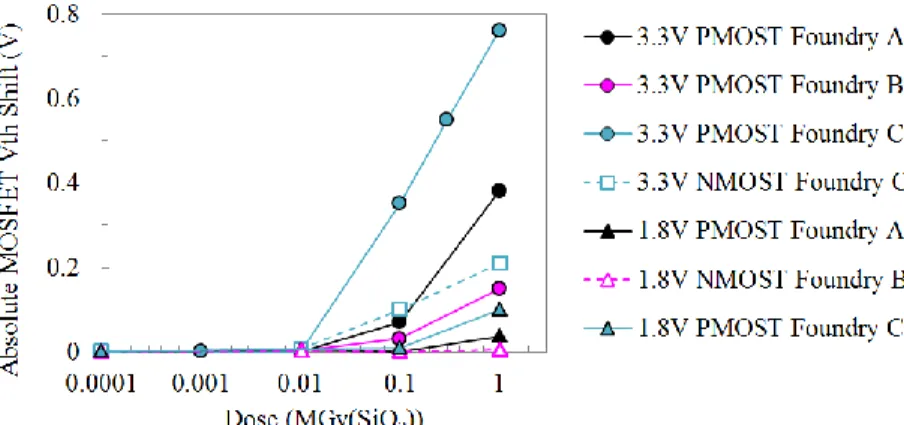
After reviewing all the possibilities, two 180 nm CIS processes (from two different foundries) have been se-lected. Indeed, this CIS technology node represents today a good tradeoff between cost, performance and availa-bility. A variety of test structures, including Metal Oxide Semiconductor Field Effect Transistors (MOSFETs) and image sensor pixel arrays have been designed and manufactured with the two selected manufacturing pro-cesses. These test structures enabled the evaluation of these manufacturing processes intrinsic radiation hardness but also of the efficiency of several radiation hardening by design techniques [4], [5]. Figure 8 presents the evo-lution of some of the studied RHBD MOSFET threshold voltages with absorbed ionizing dose for the two se-lected CIS processes. These results are also compared to those obtained on a third CIS processes (from [8]). This graph agrees with the fact that, at this TID level, P channel transistors are always much more degraded than their N-channel counterparts, as reported in [9]–[11] and that low voltage transistors (i.e. 1.8 V MOSFETs) are also much more resistant to TID than high voltage (i.e. 3.3V) ones. More importantly, this figure demonstrates the large influence of the manufacturing process on the radiation hardness with discrepancies that can reach a factor of three between foundries B and C.
Figure 8 : Evolution of the absolute threshold voltage with TID of the studied radiation-hardened-by-design MOSFETs on the two selected technologies (A and B). These results are also compared to a third technology (CIS process C) from [8]. Nominal biases were applied to
these transistors during irradiation. NMOST = N-channel MOSFET. PMOST = P-channel MOSFET.
Pixel array test structures from the two selected manufacturing processes have also been characterized before and after irradiation. Figure 9 shows an image captured before and after irradiation with the pixel array manufac-tured with the CIS process selected for the next phase of the project. The image is divided into 16 pixel sub-arrays, each with a different pixel design (most of them are radiation hardened designs). It can be seen that after irradiation some pixel designs are not functioning properly anymore (bottom left and top right regions). This image demonstrates that the imaging capability is maintained after the deposition of 1 MGy of TID on most of the explored RHBD pixels. Furthermore, the image quality and the color rendering capability are not significant-ly degraded in these rad-hard pixel regions highlighting that several solutions exist to reach the goal of CAMRAD. Thanks to the full set of results (detailed in [6]) acquired during the exploration phase, it is possible to select the most suitable technology for the development phase. The performance parameters extracted from the characterization of the studied pixel arrays are also used in the development phase to design the other subsys-tems of the camera head.
a)
b)
Figure 9 : Raw color image captured by a 128×256 pixel array test structure a) before and b) after 1 MGy(SiO2) irradiation. The tested pixel array is divided into 16 smaller arrays with differ-ent pixel layouts. Radiation hard pixel designs are the ones exhibit no significant image
degra-dations after exposure to ionizing radiation.
Optical system exploration phase outcomes
The main concern about the optical system is the darkening (or RIA for radiation induced attenuation) of its optical lenses [12]. During irradiation electrons and holes are released by ionization [13] and can be trapped by point defects causing the appearance of new absorption bands [1]. This darkening can lead to an absorption of several dB/mm in the visible spectrum [14] [15] and its amplitude and kinetics depend on a number of parame-ters such as the glass composition. Designed with COTS glasses, optical systems made with mm-thick lenses present after some kGy a darkening level that can prevent the camera to acquire exploitable images.
To prevent the darkening, the optical system will be designed with Radiation Hardened (RH) silica-based glasses that are usually doped with cerium oxide. The two oxidation states of cerium, Ce3+ and Ce4+, can trap electrons or holes helping to prevent the creation of some of the absorption bands causing the darkening [16] [17] [18]. This technique was developed in the 60s and these glasses have permanent RIA lower than 0.5 dB/mm in the visible spectrum after 1 MGy [19] [20]. Hence, by minimizing the number of lenses and choosing a suita-ble illumination system, we can maintain a sufficient light level on the CMOS image sensor.
To consider the contribution of both transient and metastable defects, online measurements under X-rays have been used to estimate the RIA levels associated to our optical system architecture [21]. By considering dose rates exceeding those expected for applications, a worst case scenario can be established as the lower the dose rate is, the lower the RIA is [22] [18]. Figure 10 presents the transmission of our optical system before and after irradia-tion. The initial transmission is close to 60% between 500 nm and 800 nm, losses being mainly due to the Fres-nel reflections on the lenses surfaces and to the transmission drop below 500 nm caused by the cerium doping. Figure 11 presents the RIA of the selected optical system architecture. The RIA above 450 nm remains below 0.2 dB, the most impacted domain concerns the blue tail of the LED spectrum associated with the illumination system.
Figure 10 : Transmission of the optical system at 0 and 1 MGy. Data are based on online measurements
at room temperature and 45 Gy(SiO2/s) under X-rays.
Figure 11 : RIA of the optical system at 1MGy. Da-ta are based on online measurements at room
Figure 12 : Effect of a 4 layers AR coating on the optical system transmission.
Figure 13 : AR coating measured in reflection at 6° at different irradiation steps.
One solution to increase the system transmission is to use Anti-Reflection (AR) coating. These coatings are based on multi-layer material designed to decrease reflections at the lens interfaces. Figure 12 illustrates the positive effect of applying an AR coating on our optical system transmission. We tested different coating tech-nologies under radiations and a typical result is presented in Figure 13. The radiation effects seem negligible or even positive: the reflection decreases with the dose.
The second worst effect of radiations on glass is the refractive index (RI) change caused by the absorption change or the density change, respectively described by the Kramers-Kronig [23] and the Lorenz-Lorentz rela-tions [24] [25]. This effect has been less studied than the darkening but literature data [19] [26] [27] provide evidence for RI changes up to 10-3.
Our optical system architecture consists in an F/6, 17°-hfov system with a focal length of 20.4 mm. The work-ing distance is 1500 mm and the observed scene is 800×450 mm. It is close to the diffraction limit (Figure 14) in terms of modulation transfer function (MTF) over the whole field. This means that its impulse response – the Point Spread Function (PSF) – is slightly bigger than the diffraction pattern of a circular aperture, known as Airy disk. The MTF is the modulus of the Fourier transform of the PSF, meaning that the smaller the PSF is, the wid-er the MTF is. The lattwid-er can be seen also as the contrast of a sinusoidal signal for a given spatial frequency (in cycles/mm). Since the pixel pitch is 𝑝 = 8.5 𝜇𝑚, the Shannon-Nyquist sampling theorem indicates that the high-est recordable spatial frequency is 𝜈𝑁𝑦=2𝑝1 which is close to 60 𝑐𝑦𝑐𝑙𝑒𝑠/𝑚𝑚 here. Higher frequencies will un-dergo aliasing.
Figure 14 : MTF of the optical system on the optical axis and for different positions in the field: half height (225 mm), half width (400 mm) and half diagonal (460 mm).
In the optical system, the RI change can induce defocusing of the image: the observed scene is blurred. This effect corresponds to an increase of the Point Spread Function diameter and thus to a MTF decrease. Figure 15 shows the MTF at 30 cycles/mm and 60 cycles/mm for a change of refractive indexes up to 10−3 for the two different radiation hardened (RH) glasses used to design it. Its performances are maintained for RI changes (Δ𝑛) lower than a few 10−4 at 60 cycles/mm. The two glasses RI changes do not have the same impact on the perfor-mances, the more impacting being the one labeled (RH2). However, if both RI changes have the same sign, their effect can partially compensate which permits to reach higher RI changes with limited performance losses.
Figure 15 : MTF at 𝝂𝑵𝒚/𝟐 (left) and 𝝂𝑵𝒚 (right) as a function of the RI change (𝚫𝒏) of two radia-tion hardened glasses (RH1 and RH2).
Illumination system exploration phase outcomes:
The illumination system is based on LEDs that are known to combine several interesting advantages : a docu-mented radiation resistance to ionizing radiation [28], a small footprint and an efficient light power emission. Even though LEDs exhibit a high tolerance to TID, other radiations can create non-radiative centers and de-crease the output light power [29].
We tested 10 white, 1 Red Green Blue (RGB) and one 1 Red Green Blue White (RGBW) LED references. An integrating sphere and a photospectrometer were used to perform spectral measurements. In Figure 16 we pre-sent two typical results, one for a white LED and one for a RGBW LED.
a)
b)
Figure 16 : Emission spectra of a) White High Power, b) RGBW LEDs before and after -rays irradiation at a TID of 1MGy.
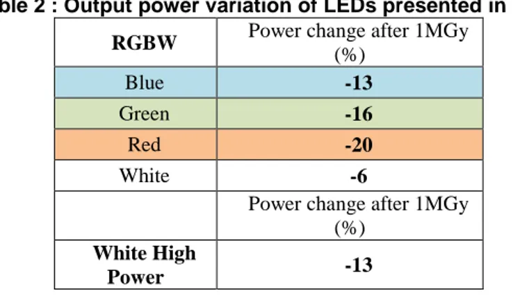
Both LEDs output powers decrease with irradiation dose; degradation levels are reported in Table 2. The final choice between the different technologies will depend on the results of the photometric calculation. A trade-off has to be made between the camera design, the image quality and the amount of light needed on the scene. The current trend leads toward a combination between High power white and RGBW LEDs. The ability of this op-tion to maintain sufficient power in every spectral channel will be assessed, as well as to adapt the amount of light power in each channel during irradiation. Temperature management also has to be taken into account, due to two opposite effects: higher temperature can act activate annealing of defects, but it is also well known that temperature decreases the output light power. For the CAMRAD project, TID-induced defects should be limited, therefore temperature management is needed to prevent the decrease of output light power.
𝚫𝒏𝟏 0 10−3 −10−3 0 10−3 −10−3 𝚫 𝒏𝟐 𝚫𝒏𝟏 0 10−3 −10−3 0 10−3 −10−3 𝚫 𝒏𝟐 0.868 0.794 0.720 0.646 0.572 0.424 0.350 0.276 0.202 0.128 0.736 0.663 0.589 0.515 0.442 0.368 0.295 0.221 0.074 0.000
Table 2 : Output power variation of LEDs presented in Figure 16
RGBW Power change after 1MGy
(%)
Blue -13
Green -16
Red -20
White -6
Power change after 1MGy (%)
White High
Power -13
Conclusion and On-Going Work
This paper presents the CAMRAD project and the key outcomes of its exploration phase. These results already demonstrate that solutions exist to build a multi MGy radiation hard color imaging system for dismantling opera-tions. This first comprehensive study of the TID effects on each camera sub-system enables the selection of the most efficient technologies to achieve the targeted imaging performances. This work also allows extrapolating some first specifications for the final imaging system prototype as illustrated in Table 3.
The next phase of the project will consist in exploiting the conclusions presented here to design each sub-system while assuring the targeted level of radiation hardness and performance. In 2019, these sub-sub-systems will be integrated into the camera prototype that shall be validated by the in-situ test. In the end, the developed radia-tion hard imaging system and its building blocks could benefit to a wide range of applicaradia-tions where it is neces-sary to observe in a harsh radiation environment, such as nuclear power plant inspection and monitoring or such as space exploration.
Table 3 : CAMRAD camera prototype targeted/expected performance (valid after exposure to the highest TID level).
Parameter/Feature Targeted/expected value
Format 1280×720 pixels
Frame rate 25 fps
Dynamic range > 60 dB
Dark current (22°C) < 0.5 pA
ADC resolution 10 bit
Color RBG bayer pattern color filter array
Failure TID > several MGy(SiO2), to be determined during the
final validation phase
References
[1]
S. Girard et al., « Radiation Effects on Silica-Based Optical Fibers: Recent Advances and Future Challeng-es », IEEE Trans. Nucl. Sci., vol. 60, no 3, p. 2015‑2036, juin 2013.[2] S. Girard et al., « Multi-MGy Radiation Hardened Camera for Nuclear Facilities », Proc. ANIMMA 2015, Lisbon, Portugal, juin-2015.
[3] V. Goiffon et al., « Radiation Hardening of Digital Color CMOS Camera-on-a-Chip Building Blocks for Multi-MGy Total Ionizing Dose Environments », janv-2017.
[4] F. Faccio, « Design Hardening Methodologies for ASICs », in Radiation Effects on Embedded Systems, Springer Netherlands, 2007, p. 143‑160.
[5] H. L. Hughes et J. M. Benedetto, « Radiation effects and hardening of MOS technology: devices and cir-cuits », IEEE Trans Nucl Sci, vol. 50, p. 500‑501, juin 2003.
[6] S. Rizzolo et al., « Radiation Hardness Comparison of CMOS Image Sensor Technologies at High Total Ionizing Dose Levels », IEEE Trans Nucl Sci, Submitted for publication.
[7] D. Contarato, P. Denes, D. Doering, J. Joseph, et B. Krieger, « High Speed, Radiation Hard CMOS Pixel Sensors for Transmission Electron Microscopy », Phys. Procedia, vol. 37, p. 1504‑1510, 2012.
[8] V. Goiffon et al., « Total Ionizing Dose Effects on a Radiation-Hardened CMOS Image Sensor Demonstra-tor for ITER Remote Handling », IEEE Trans. Nucl. Sci., vol. 65, no 1, p. 101‑110, janv. 2018.
[9] F. Faccio et G. Cervelli, « Radiation-induced edge effects in deep submicron CMOS transistors », IEEE Trans Nucl Sci, vol. 52, no 6, p. 2413–2420, déc. 2005.
[10] V. Goiffon et al., « Multi-MGy Radiation Hard CMOS Image Sensor: Design, Characterization and
X/Gamma Rays Total Ionizing Dose Tests », IEEE Trans. Nucl. Sci., vol. 62, no 6, p. 2956‑2964, déc. 2015. [11] F. Faccio, S. Michelis, D. Cornale, A. Paccagnella, et S. Gerardin, « Radiation-Induced Short Channel
(RISCE) and Narrow Channel (RINCE) Effects in 65 and 130 nm MOSFETs », IEEE Trans. Nucl. Sci., vol. 62, no 6, p. 2933‑2940, déc. 2015.
[12] M. Fruit, A. I. Gusarov, D. B. Doyle, et G. J. Ulbrich, « Radiation impact on spaceborne optics: the dose coefficients approach », 1999, p. 60.
[13] P. W. Levy, « Overview Of Nuclear Radiation Damage Processes: Phenomenological Features Of Radiation Damage In Crystals And Glasses », 1985, p. 2.
[14] I. Manolis et al., « The ESA RADGLASS activity: a radiation study of non rad-hard glasses », présenté à Sensors, Systems, and Next-Generation Satellites XIX, Toulouse, 2015, vol. 9639, p. 1 96391N-15.
[15] D. Doyle, « Radiation-induced transmission degradation of borosilicate crown optical glass from four dif-ferent manufacturers », Opt. Eng., vol. 46, no 4, p. 043004, avr. 2007.
[16] A. M. Bishay, « Role of Cerium in Suppression of Gamma-Ray Induced Coloring of Borate Glasses », J. Am. Ceram. Soc., vol. 45, no 8, p. 389‑393, août 1962.
[17] X. Fu, L. Song, et J. Li, « Radiation induced color centers in cerium-doped and cerium-free multicomponent silicate glasses », J. Rare Earths, vol. 32, no 11, p. 1037‑1042, nov. 2014.
[18] S. Baccaro, A. Cemmi, I. Di Sarcina, et F. Menchini, « Gamma Rays Effects on the Optical Properties of Cerium-Doped Glasses », Int. J. Appl. Glass Sci., vol. 6, no 3, p. 295‑301, sept. 2015.
[19] T. Allanche et al., « Vulnerability and Hardening Studies of Optical and Illumination Systems at MGy Dose Levels », IEEE Trans. Nucl. Sci., vol. 65, no 1, p. 132‑140, janv. 2018.
[20] SCHOTT, « Radiation Resistant Optical Glasses », TIE-42, août 2007.
[21] S. Girard et al., « Growth and Decay Kinetics of Radiation-Induced Attenuation in Bulk Optical Materi-als », IEEE Trans. Nucl. Sci., p. 1‑1, 2017.
[22] M. Van Uffelen, « Modélisation de systèmes d’acquisition et de transmission à fibres optiques destinés à fonctionner en environnement nucléaire », PhD thesis, Université de Paris XI, France, 2001.
[23] A. I. Gusarov et al., « Refractive-index changes caused by proton radiation in silicate optical glasses », Appl. Opt., vol. 41, no 4, p. 678–684, 2002.
[24] A. Morana, « Gamma-rays and neutrons effects on optical fibers and Bragg gratings for temperature sen-sors », Saint Etienne, 2013.
[25] C. Muller et al., « Potential performance loss and compensation techniques of a lens under ionizing radia-tions », p. 11.
[26] A. I. Gusarov et D. B. Doyle, « Radiation-induced wave-front aberrations: a new approach », Appl. Opt., vol. 37, no 4, p. 643–648, 1998.
[27] D. Doyle, « Radiation Hardeness of Optical Materiel », 3rd Europa Jupiter System Mission Instrument Workshop, ESA ESTEC, Noordwijk, janv-2010.
[28] A. H. Johnston, « Radiation damage of electronic and optoelectronic devices in space », Proceedings of the 4th International Workshop on Radiation Effects on Semiconductor Devices for Space Application, 2000. [29] G. A. Umana-Membreno et al., « 60Co gamma-irradiation-induced defects in n-GaN », Appl. Phys. Lett.,