Science Arts & Métiers (SAM)
is an open access repository that collects the work of Arts et Métiers Institute of Technology researchers and makes it freely available over the web where possible.
This is an author-deposited version published in: https://sam.ensam.eu Handle ID: .http://hdl.handle.net/10985/10360
To cite this version :
M NISTOR, E MILLON, C CACHONCINLLE, Wilfrid SEILER, N. JEDRECY, C HEBERT, J. PERRIERE - Transparent conductive Nd-doped ZnO thin films - Journal of Physics D: Applied Physics - Vol. 48, p.195103 (9pp) - 2015
Any correspondence concerning this service should be sent to the repository Administrator : [email protected]
1. Introduction
Due to its specific electrical and optical properties (high elec-trical conductivity and high optical transparency in the visible domain), zinc oxide (ZnO) is a suitable material with appli-cations in a large number of devices and components such as optical waveguides, piezoelectric transducers, transparent conductive electrodes, gas sensors, light emitting diodes, and others [1–6]. Moreover, because it is abundant and environ-mentally friendly, ZnO is an ideal wide bandgap material for applications in photovoltaics (PV). The ability to easily tune the conductivity, charge carrier concentration, and optical properties of ZnO films is highly desirable for these applica-tions. Doping by well-suited elements is a way to modify or
enhance physical properties or to induce new ones in oxide films [5–9]. In this frame, the best doping of ZnO thin films for both electrical conductivity and optical transparency com-parable with those of the indium-tin oxide (ITO) films was achieved by group III [7], group IV [8], or other elements (Sc, Y) [9]. Such properties have been attributed to the ionic radius of Al3+, Sc3+, and Y3+ elements close to that of Zn2+ or even
smaller (Ga3+) [9].
In view of specific PV applications, such as solar energy converters for Si solar cells, rare Earth (RE) elements such as Nd, Yb, or Eu doping in ZnO or in other oxide materials were used to obtain down-shifting effects [10–14]. More specifi-cally, the effects of incorporation of Nd3+ ions on the
struc-ture, microstrucstruc-ture, and chemical nature of Nd-doped ZnO
Transparent conductive Nd-doped
ZnO thin films
M Nistor1, E Millon2, C Cachoncinlle2, W Seiler3, N Jedrecy4,5, C Hebert4,5 and J Perrière4,5
1 National Institute for Lasers, Plasma and Radiation Physics (NILPRP), L22 PO Box. MG-36, 77125 Bucharest-Magurele, Romania
2 GREMI, UMR 7344 CNRS-Université d’Orléans, 45067 Orléans Cedex 2, France
3 PIMM, UMR CNRS 8006 Arts et Métiers ParisTech, 151 Boulevard de l’Hopital, 75013 Paris, France 4 Sorbonne Universités, UPMC Univ Paris 06, UMR 7588, INSP, F-75005, Paris, France
5 CNRS, UMR 7588, INSP, F-75005, Paris, France
E-mail: [email protected] and [email protected]
Abstract
Transparent Nd-doped ZnO films with thickness in the range of 70 to 250 nm were grown by pulsed-laser deposition (PLD) on c-cut sapphire substrates at various oxygen pressures and substrate temperatures. A wide range of optical and electrical properties of the films were obtained and correlated to the composition and crystalline structure. The Nd-doped ZnO films are smooth, dense, and display the wurtzite phase. Different epitaxial relationships between films and substrate as a function of growth pressure and substrate temperature were evidenced by asymmetric x-ray diffraction measurements. By varying PLD growth conditions, the films can be tuned to have either metallic or semiconductor characteristics, with good optical transmittance in the visible range. Moreover, a low-temperature metal-insulator transition may be observed in Nd-doped ZnO films grown under low oxygen pressure. Resistivities as low as 6 × 10⁻⁴ Ω cm and 90% optical transmittance in the visible range and different
near-infrared transmittance are obtained with approximately 1.0–1.5 at.% Nd doping and growth temperature of approximately 500 °C.
Keywords: zinc oxide, pulsed laser deposition, thin films, optical properties, electrical properties, metal-insulator transition
(Some figures may appear in colour only in the online journal) M Nistor et al Printed in the UK 195103 JPD © 2015 IOP Publishing Ltd 2015 48
J. Phys. D: Appl. Phys.
JPD
0022-3727
10.1088/0022-3727/48/19/195103
Papers
19
Journal of Physics D: Applied Physics HT
thin films were investigated [15–17]. For limited Nd-doping concentration (a few %), the hexagonal ZnO wurtzite struc-ture with a preferential orientation (c-axis texstruc-ture) is preserved with a variation of the c-axis parameter because of the differ-ence in ionic radii of Nd3+ and Zn2+. In addition, x-ray
photo-electron spectroscopy (XPS) and near-edge x-ray absorption fine structure (NEXAFS) measurements reveal that Nd spe-cies are in the trivalent state and occupy Zn site in the network [15, 16]. Such Nd-doped ZnO films were highly transparent in the visible wavelength domain, and the energy bandgap was found to depend not only on the Nd doping level but also on the deposition process and conditions [10, 18]. The lumi-nescence properties of Nd3+ ions in ZnO were studied [15,
19], and intense luminescence indicating infrared emission of Nd3+ in ZnO was observed. The direct excitation of Nd3+ ions
in the ZnO matrix was possible, and an intense signal was also observed when the ZnO host was excited by UV light. This demonstrates the existence of a transfer mechanism between the ZnO host and Nd3+ ions [15, 19], i.e. Nd-doped ZnO films
could act as an efficient downshifter in PV devices [19]. The electronic structure of RE-doped ZnO was investigated by first principles calculations [20, 21]. It was concluded from these theoretical simulations that n-type doping is present in Nd-doped ZnO because the donor states are located near the conduction band [20, 21]. However, despite these theoretical simulations indicating that Nd3+ ions could be carrier donors,
the electrical properties of Nd-doped ZnO films have not been systematically studied. Thus, the possibility of obtaining mul-tifunctional ZnO films by Nd doping, i.e. both transparent conducting electrodes and solar energy converter, has not yet been precisely explored. With this aim, the first step was to investigate in detail the effects of Nd doping on the transport and optical properties of zinc oxide films.
In this work, pulsed-laser deposition (PLD) was used to obtain transparent and conductive Nd:ZnO films. PLD is well-adapted for the growth of dense, uniform, and epitaxial oxide films with complex compositions. The Nd:ZnO films were grown on c-cut sapphire substrates at various oxygen pres-sures and substrate temperatures. By the complementary use of Rutherford backscattering spectrometry and x-ray diffrac-tion analyses, the composidiffrac-tion and structure of the films were determined. The effects of the composition on the structural characteristics of the films were correlated to their optical and electrical properties.
2. Experimental
The films were grown onto c-cut sapphire substrates by PLD using a frequency quadrupled Nd:YAG laser delivering pulses (10 ns, 100 mJ cm−2) irradiating an Nd-doped ZnO ceramic target (1% at. Nd). The experimental setup was previously described [22, 23]. Film growth was performed under con-trolled pressure between residual vacuum (10−6 mbar) up to 10−1 mbar oxygen pressure. The substrate temperature was varied in the range of 300–700 °C. After the growth, the films were cooled to room temperature (RT) at the oxygen pressure used during film deposition.
The thickness and composition of films were determined by Rutherford backscattering spectrometry (RBS) using 2 MeV 4He+ ion beam. These RBS measurements were
per-formed under the Convention for SAFIR@ALTAÏS between the Université Pierre et Marie Curie and the University of Namur”. The RBS spectra were interpreted using the RUMP simulation program to determine the precise oxygen and cati-onic composition and their in-depth variations. The accuracy of the oxygen composition deduced from the RBS analysis is estimated to be 4%. X-ray diffraction (XRD) analysis with a four-circle diffractometer with the Cu Kα radiation
(λ = 0.154 nm) from PIMM-Arts et Metiers ParisTech in Paris
was used to determine the nature of the crystalline phase and lattice parameters. Rocking curve measurements and asym-metric diffraction (pole figure measurements) were performed to determine the film texture and epitaxial relationships with the substrate.
The electrical properties (resistivity as a function of tem-perature from liquid helium up to 300 K) were obtained by the classical four probe method. The nature, concentration, and mobility of charges were determined with a MMR Hall measurement system (in the van der Pauw geometry) at room temperature (RT) and under a magnetic field of 0.3 T. The transmittance of the films was measured with a spectropho-tometer Cary 5000 in the wavelength range of 190–3200 nm.
3. Results and discussion
The compositions of the Nd-doped ZnO films are summarized in the table 1. Values of Nd concentrations are in the range of 1 to 1.5% at., i.e. a priori small values sufficient to avoid the formation of large Nd or Nd2O3 clusters in a ZnO matrix. PLD
under low oxygen pressure allows the formation of oxygen-deficient oxide films [24, 25], but Nd-doping does not seem to play a specific role in oxygen composition because undoped ZnO films grown in the same conditions show a similar behavior as indicated in table 1.
The θ–2θ XRD patterns from all films (not presented here)
only show the (0 0 2) peak of the wurtzite structure, whatever the oxygen and Nd concentrations, meaning that the films are highly c-axis–textured. The corresponding c-axis parameters are given in table 1 and show rather large variations by com-parison with the values observed on undoped zinc oxide films. In the same way the full width at half maximum (FWHM) of (0 0 2) rocking curves are significantly larger than the ones measured on undoped films, Nd can be incorporated by sub-stitution of Zn or in an interstitial position in the wurtzite ZnO lattice. Results from the NEXAFS study show strong evidence for hybridization of Nd ions with O in the ZnO lattice [15]. This study also indicates that trivalent Nd ions occupy diva-lent Zn sites. Because of the difference in ionic radii (0.098 and 0.074 nm), this doping induces structural disorder, whose importance will also be related to the growth conditions, as shown by the values of the FWHMs. As expected, the increase in growth temperature leads to a decrease of the FWHM, i.e. a better crystalline state in the films. In the doped films, the decrease of the structural disorder when raising the growth
temperature is enhanced by the fact that RE3+ are no longer
incorporated in the ZnO lattice but are segregated at grain boundaries [26].
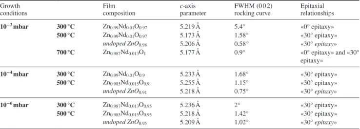
Despite the high values of the film mosaicity (see table 1, FWHM of (0 0 2) rocking curve), the epitaxy of the films was checked. The (103) pole figures of ZnO (2θ = 62.8°) were
recorded and typical results are presented in figures 1(a)–(c) (corresponding to growths under 10−2 mbar at 300, 500 and 700 °C). Such measurements evidence the epitaxial Nd:ZnO film growth on sapphire substrates via the presence of well-defined poles at declination angle Ψ = 31.8°, corresponding to the (103) ZnO reflexions. In addition, three other poles are observed at Ψ value 18.8°, corresponding to the (018) reflex-ions of the sapphire substrate (2θ = 61.3°). Such poles allow
us to determine the epitaxial relationships between the film and substrate as a function of the growth conditions.
At 300 °C and 10−2 mbar (figure 1(a)), the following
in-plane epitaxial relationship is deduced:
ZnO [100] // Al O [100]2 3
This in-plane orientation corresponds to the direct superposi-tion of the hexagons of the (0 0 1) basal planes of ZnO and c-cut sapphire substrate, i.e. a hexagon on hexagon epitaxy (labeled ‘0° epitaxy’), although the respective in-plane axis parameters of the film and substrate are largely different (more than 30%). This can be interpreted in the frame of domain matching [27], where 3 ZnO lattice units match with 2 sapphire lattice units, leading to a lattice mismatch equal to 5.8%. This ‘0° epitaxy’ has been observed on undoped ZnO films grown on sapphire at a low substrate temperature and a high deposition rate [28].
At higher temperatures (figure 1(b) for a film grown at 500 °C), the in-plane epitaxial relationships is:
ZnO [100] // Al O [210]2 3
This orientation corresponds to the usual epitaxy reported for the growth of undoped ZnO films on c-cut sapphire sub-strate [28, 29] at substrate temperatures higher than 500 °C. It corresponds to a 30° rotation of the ZnO hexagons of the (0 0 1) basal plane with respect to those of sapphire, i.e. a ‘30°
epitaxy’. In the frame of the domain matching epitaxy, two distinct possibilities may be considered: either the coinci-dence of 7 Al2O3 lattice units with 6 ZnO lattice units or the
coincidence of 6 and 5 lattice units, leading to a lattice mis-match of 1.38 and 1.43%, respectively. It has been found that these two epitaxial domains (7–6 and 6–5) are both present in undoped ZnO films to accommodate the lattice mismatch [27]. By comparison with the lattice mismatch of the ‘0° epitaxy’, this ‘30° epitaxy’ looks much more favorable. Moreover, the hexagonal close-packed oxygen sub-lattices in both sapphire substrate and zinc oxide film have an identical in-plane orien-tation [27, 29], ensuring a continuity of the oxygen network through the film-substrate interface.
For the film grown at 700 °C and 10−2 mbar (figure 1(c)),
12 (103) poles are observed; six of them correspond to the 0° epitaxy and the other six poles are characteristics of the 30° epitaxy. The presence of these two distinct epitaxial relation-ships has not been reported in the case of undoped ZnO films grown with similar substrate temperatures. The presence of Nd in the film is therefore at the origin of the existence of the two epitaxial relationships.
In the ‘0° epitaxy’, the minimum size of the epitaxial domain deduced from the lattice matching is rather limited, i.e. 3 ZnO lattice units approximately 1 nm. On the contrary, for the ‘30° epitaxy’, the corresponding minimum size of the domain is much higher, i.e. 5 or 6 ZnO lattice units approxi-mately 3 nm. For T < 300 °C, the surface diffusion of the incident species is low, and the small-size epitaxial domain will be favored in these conditions, i.e. the ‘0° epitaxy’ will be observed despite the unfavorable lattice mismatch. For increasing temperatures, the incident species will diffuse on longer distances, allowing the formation of larger epitaxial domains, i.e. the ‘30° epitaxy’ will be observed for T = 500 °C.
At 700 °C, a new parameter associated with the presence of Nd in the film has to be considered. At such high T, Nd3+ ions
are no longer incorporated in the ZnO lattice. The large Nd3+
ions act as grain growth inhibitors and aggregate at the grain boundaries [26]. In this case, the Nd ions will partly limit the size of the epitaxial domain because they will not take part in
Table 1. Film composition (deduced from RBS), values of the c-axis parameter, and FWHM of the (0 0 2) rocking curve for the Nd-doped ZnO films grown under various conditions. The epitaxial relationships with the sapphire substrate are summarized (for comparison purposes, some corresponding values for undoped ZnO films are also presented).
Growth
conditions Film composition cparameter-axis FWHM (0 0 2) rocking curve Epitaxial relationships
10−2 mbar 300 °C Zn0.99Nd0.01O0.97 5.219 Å 5.4° «0° epitaxy»
500 °C Zn0.99Nd0.01O0.97 5.173 Å 1.58° «30° epitaxy» undoped ZnO0.98 5.206 Å 0.58° «30° epitaxy»
700 °C Zn0.987Nd0.013O1 5.177 Å 0.9° «0° epitaxy» and «30° epitaxy»
10−4 mbar 300 °C Zn0.99Nd0.01O0.9 5.233 Å 1.68° «30° epitaxy»
500 °C Zn0.985Nd0.015O0.9 5.255 Å 1.15° «30° epitaxy» undoped ZnO0.91 5.218 Å 0.75° «30° epitaxy»
10−6 mbar 300 °C Zn0.987Nd0.013O0.95 5.236 Å 2° «30° epitaxy»
500 °C Zn0.985Nd0.015O0.95 5.218 Å 1.42° «30° epitaxy» undoped ZnO0.95 5.209 Å 1.02° «30° epitaxy»
the ZnO lattice formation. For 1% Nd doping, the distance between Nd3+ ions assuming a random distribution is
approxi-mately 1.3 nm. This average distance is thus located between the small ‘0° epitaxy’ domain size and the large ‘30° epitaxy’ domain size. It follows that the formation of large-size ‘30° epitaxy’ domains will be limited by some Nd3+ ions, whereas
the small-size ‘0° epitaxy’ domain will not be limited by the Nd3+ ions. Therefore, both epitaxial relationships are present
at 700 °C despite the unfavorable lattice mismatch of the ‘0° epitaxy’.
The different epitaxial relationships are summarized in table 1, together with those obtained for Nd-doped ZnO films grown at 300 and 500 °C under 10−4 and 10−6 mbar oxygen
pressures, which only present the 30° rotation in-plane epi-taxial relationships, in agreement with the results obtained on undoped zinc oxide films.
Optical transmittance measurements were performed in the range of 190–3200 nm for Nd-doped ZnO films grown under 10−2 mbar at 300, 500 and 700 °C (figure 2) and under 10−4 and 10−6 mbar at 300 and 500 °C (figure 3), respectively. These films are optically transparent in the visible range, although the polished c-cut sapphire substrate contributes to these measurements. The film grown at 10−2 mbar and 300 °C strongly absorbs in the near-infrared region (NIR), whereas the films at 500 and 700 °C have high transmittance in this region (figure 2). It is interesting to note that Nd:ZnO films grown at low oxygen partial pressures (10−4 and 10−6 mbar)
Figure 1. Pole figure for the (103) ZnO recorded on films grown under 10−2 mbar on sapphire substrates held at (a) 300 °C, (b) 500 °C, and (c) 700 °C.
Figure 2. UV-vis-near IR transmittance for Nd-doped ZnO films grown under 10−2 mbar at 300, 500 and 700 °C. The inset shows the corresponding Tauc plots.
Figure 3. UV-vis-near IR transmittance for Nd-doped ZnO films grown under 10−4 and 10−6 mbar at 300 and 500 °C. The inset shows the corresponding Tauc plots.
are oxygen-deficient (table 1) but maintain high optical trans-mittance in visible and NIR (figure 3). This high optical trans-mittance up to NIR is required for transparent conductive oxide (TCO) on Si or multijunction solar cells [5] despite that most of the TCO thin films present an absorption in NIR due to the doping level and free carrier absorption.
The absorption coefficient (α) was calculated using the
relation α = (1/d)ln[(1 − R)/T], where T is the transmittance, R is the reflectance (neglected here), and d is the film thick-ness. The insets in figures 2 and 3 show the Tauc’s plots, i.e. (αE)2 versus E, where E is the photon energy and α is the
optical absorption coefficient. Nd-doped ZnO films have a direct bandgap (Eg), which was obtained by extrapolating
the linear part of the absorption edge to the intersection with the energy axis. As shown in table 2, for the films grown at 10−2 mbar, the bandgap value decreases with improving crystallinity of films, from 3.35 eV at 300 °C to 3.26 eV at 700 °C. The same tendency is observed for oxygen-defi-cient films grown at 10−4 and 10−6 mbar (table 2) but with bandgap values slightly higher than those corresponding to near-stoichiometric films grown at 10−2 mbar. Recently, a decrease in the bandgap from 3.22 to 3.14 eV was observed for Nd-doped ZnO thin films grown on glass substrates by spray pyrolysis method, when the Nd concentration increased up to 5% [10].
From the transmittance spectra (figures 2 and 3) it is pos-sible to extract values of the optical resistivity, concentration, and mobility of the carriers, and then correlate them with measured electrical properties by the Hall effect [9, 30–34]. The measured transmittance spectra of films were fitted by the calculated transmittance from a dielectric model using Scout commercial software, which includes several built-in optical models [33–35]. An interband transition model of the absorption edge and the extended Drude free electron model for the free carriers were used, as applied previously for dif-ferent doped ZnO thin films [30–33]. The simulated optical
resistivity ρopt, mobility μopt, and electron concentration nopt
are presented in table 2.
The resistivity of the films, the carrier concentration, and mobility were also determined by Hall measurements. Table 3 summarizes these results, together with the thickness of the films. Comparable variations for the resistivity are obtained with the two measurements. It can be concluded from tables 2 and 3 that a wide range of resistivity (between 10−4 Ω cm and 4 × 10⁻² Ω cm) of the Nd-doped ZnO thin films are obtained as
a function of growth pressure and substrate temperature during PLD. In comparison, for the Nd-doped ZnO films grown by spray pyrolysis the lowest resistivity value was approximately 4.0 10−2 Ω cm for 1% Nd effective doping [10]. Some differ-ences appear between the optical and Hall measurements, as already observed for doped ZnO films [30]. The optical trans-mittance is a measurement of the overall material, whereas Hall measurements can only check conductive paths in the film and are more affected by scattering mechanisms [4, 31, 32]. In table 3, some values of resistivity, mobility, and car-rier concentration (indicated by *) present a noticeable inac-curacy (30%). Such difficulty deducing precise values from Hall measurements already has been reported in the case of non-homogeneous oxide films [36]. In the present case, this should be related to the possible Nd (or Nd2O3) segregation in
ZnO at high temperatures.
The Haacke figure of merit was used to compare the prop-erties of Nd-doped ZnO films with other TCO films, as exem-plified elsewhere [4]: ΦH= TR =T σd s 10 10 (1) where T is the transmittance for the wavelength of 550 nm in the visible range and without contribution of the sub-strate, Rs is the sheet resistance, σ is the electrical
conduc-tivity (σ = 1/ρ, where ρ is the resistivity determined from Hall
Table 2. Values of the optical band gap, resistivity, density, and mobility of carriers deduced from the optical measurements on Nd-doped ZnO films grown on sapphire substrates under various conditions.
Pressure 10−2 mbar 10−4 mbar 10−6 mbar
Tsubstrate 300 °C 500 °C 700 °C 300 °C 500 °C 300 °C 500 °C
Eg (eV) 3.35 eV 3.31 eV 3.26 eV 3.43 eV 3.33 eV 3.47 eV 3.39 eV
ρopt (Ωcm) 1.25 10−3 9.30 10−3 4.85 10−2 2.39 10−3 5.16 10−3 2.09 10−3 3.06 10−3
µopt (cm2 Vs−1) 19.57 7.73 0.2 8.65 8.56 7.03 7.63
nopt (cm−3) 2.55 1020 8.69 1019 6.53 1020 3.02 1020 1.41 1020 4.25 1020 2.68 1020
Table 3. Values of the resistivity, density, and mobility of carriers deduced from Hall measurements on Nd-doped ZnO films grown on sapphire substrates under various conditions (the figures of merit are also presented).
Pressure 10−2 mbar 10−4 mbar 10−6 mbar
Tsubstrate 300 °C 500 °C 700 °C 300 °C 500 °C 300 °C 500 °C Thickness(nm) 240 nm 144 nm 76 nm 92 nm 64 nm 95 nm 72 nm ρ (Ωcm) 1.35 10−3 4.34 10−2 6.96 10−2 7.57 10−4 1.38 10−3 6.03 10−4 7.30 10−4 µ (cm2 Vs−1) 25.29 3.77 29.24* 35.62 1.93* 36.45 13.02* n (cm−3) 1.83 1020 3.82 1019 3.07 1018* 2.32 1020 2.34 1021* 2.8 1020 6.54 1020* ΦH (Ω−1) 1.05 10−2 2.68 10−4 7.34 10−5 5.84 10−3 3.22 10−3 7.88 10−3 6.71 10−3
measurements), and d is the film thickness. The exponent 10 of the transmittance corresponds to a transmittance (90%) that is sufficient for most applications. The results are shown in table 3, evidencing that Nd-doped ZnO thin films show a wide range of figures of merit, varying from comparable with those of thin metal films (~10−4–10−5 Ω−1) to comparable with
those of ITO films (~10−2–10−1 Ω−1) or ZnO/metal/ZnO films
(~10−2 Ω−1) [4].
As previously noted, the NEXAFS study indicates that trivalent Nd ions occupy divalent Zn sites, resulting in addi-tional charge carriers [15]. It is thus interesting to compare the carrier concentrations with the theoretical values calcu-lated by assuming that each Nd which is substituted to Zn gives one electron in agreement with its 3+ oxidation state (with respect to the Zn2+). For example, at 10−2 mbar and
300 °C, films close to the ZnO stoichiometry are formed (see table 1); therefore, the presence of extra electrons given by oxygen vacancies can a priori be excluded. It follows that the theoretical carrier concentration given by Nd ions would be 4.15 × 1020 cm−3 to compare with the experimental value
of 1.83 × 1020 cm−3. This means that at 300°C, 44% of the
Nd dopant seem to be active, but this concentration decreases with increasing temperature, reaching nearly zero at 700 °C in conditions where Nd doping is no longer in substitution of Zn in the zinc oxide network. At 10−4 and 10−6 mbar, the films are largely oxygen-deficient (table 1), meaning that oxygen vacancies furnish electrons for the film conductivity. The effects of such vacancies are very important at 500 °C, as shown in tables 2 and 3.
In undoped ZnO, for carrier concentrations higher than 3 to 5 × 1019 cm−3, the merging of the impurity band (originally
giving rise to the Burstein Moss behavior) with the conduction band occurs, causing a change in the electrical transport prop-erties of ZnO from semiconductor to metal behavior at RT [37]. Tables 2 and 3 show that the electron density measured in the Nd-doped films are often higher than this critical den-sity, and thus a metallic behavior is expected for these films. To check this point, resistivity measurements as a function of temperature (ρ(T) curves) were performed; these results are
reported in figures 4 and 5.
Figure 4 shows the ρ(T) curves for the films grown at 10−4
and 10−6 mbar oxygen pressure. Starting from 300 K and low-ering the temperature, these curves present a positive tempera-ture coefficient of resistivity (TCR) that is characteristic of a metallic behavior up to a critical temperature below which the TCR becomes negative. Except for the film grown at 300 °C and 10−6 mbar, which remains metallic down to liquid helium, the temperature of the metal-insulator transition (MIT) is in the range of 98–140 K.
This crossover from metal to insulator at a specific tem-perature has been observed in various oxide films [7, 29, 38–40], presenting both a high carrier concentration leading to a degenerate semiconductor (metallic behavior) and a suf-ficient structural disorder leading to multiple scattering of the carriers [41]. The increase of the resistivity below the MIT critical temperature can be interpreted in the frame of the quantum corrections to the conductivity (QCC) to the semi-classical Boltzmann approach [41, 42]. In this approach, the
Figure 4. Temperature -dependent resistivity of Nd-doped ZnO films grown under (a) 10−4 at 300 °C, (b) 10−4 mbar at 500 °C, (c) 10−6 mbar at 300 °C, and (d) 10−6 mbar at 500 °C.
resistivity ρ(T) as a function of T can be simulated using the
following function that takes into account the QCC and the Boltzmann transport equation:
ρ σ = + + + T a T a T bT ( ) p1 0 1 /2 2 1/2 2 (2)
where σ0 is the residual resistivity (σ0=1/ );ρ0 a T1 p/2anda T2 1/2
are the QCC terms corresponding, respectively, to the weak localization (WL) effect (a Tp )
1 /2 and Coulomb interaction
effect (a T2 1/2) in the case of a 3D dimension film [41]; and bT2
is the usual semiclassical transport Boltzmann term. The value of p depends on the type of interactions, with b being equal to 2 for electron–electron or 3 for electron–phonon interactions, respectively [41].
Equation (2) was used to fit the various ρ(T) curves
pre-senting a MIT, and the simulated curves (continuous line) are presented in figure 4, superimposed to the experimental curves. The values of the fit parameters are given in table 4. In the fitting procedure, p was considered as a free parameter, and the best adjustment (p ~ 3) corresponds to the electron– phonon interaction because it has been obtained previously in the case of undoped ZnO disordered thin films [29, 43] grown by pulsed electron beam deposition [44]. For the Nd-doped
ZnO film grown at 10−6 mbar and 500 °C, the values of a1 and a2 lead to the conclusion that the main contribution to the QCC comes from the Coulomb interaction, whereas the effect of the WL is less pronounced [41, 42]. For the Nd-doped ZnO films grown at 10−4 mbar, a1 >> a2, which means that the main
con-tribution to the QCC comes from the WL term, whatever the substrate temperature.
This interpretation of the ρ(T) curves, based on the QCC, is
applicable under the condition that the correction term based on the WL and Coulomb interaction only represents a small fraction of the residual resistivity. To check this point, the max-imum value of the ratio of δσ/σ0 (where δσ =a T1 p/2+ a T2 1/2)
was calculated; for the three curves showing MIT, this ratio is much smaller than 0.03 at 50 K, justifying the treatment.
The presence of MIT in the films is due to the high density of carriers (metallic behavior) and to the structural disorder present in the films (scattering of the carriers). Such an MIT is not observed in the undoped zinc oxide films grown by PLD in the same conditions; therefore, Nd doping plays a major role in both the carrier concentration and the structural disorder. For this last point, although epitaxial relationships have been evidenced between film and substrate, the presence of defects (atomic defects, cell distortion ...) is deduced from the c-axis parameter variations and the large values of the FWHMs. The origin of these structural defects is, first, the Nd doping of the films (as seen before) and, second, the presence of a high con-centration of oxygen vacancies in the films grown at 10−4 and 10−6 mbar. Both contribute to the formation of a disordered medium that leads to an efficient scattering of the carriers and to localization effects.
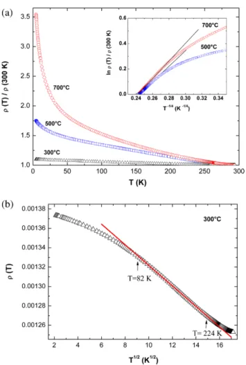
Figure 5(a) shows temperature-dependent resistivity normalized at 300 K of Nd-doped ZnO films grown under 10−2 mbar oxygen pressure and various substrate tempera-tures. The three curves present a negative TCR in the whole temperature range, which is typical behavior for a semicon-ductor. However, the ratio of resistivity at helium liquid to that measured at 300 K is less than 4. Such curves cannot be fitted by an Arrhenius plot, i.e. this small increase in resis-tivity cannot be explained by a classic activated transport mechanism for semiconductors. Because of the high values of carrier concentration in these films, this could mean that such films are in the insulating side of the MIT, i.e. the tran-sition temperature of the MIT would be higher than 300 K. This point has been checked for the film grown at 300 °C. The resistivity as a function of T0.5 presented in figure 5(b)
shows a linear variation in a wide temperature range. Such
Figure 5. (a) Normalized ρ(T)/ρ(300 K) curves for films grown under 10−2 mbar at 300, 500, and 700 °C. The inset shows ln(ρ(T)/ρ(300 K)) as a function of (1/T)1/4 for the 500 and 700 °C curves (b) normalized ρ(T)/ρ(300 K) as a function of T1/2 for the 300 °C curve.
Table 4. Values of the fit parameters giving the best adjustment for the simulation of the ρ(T) curves using equation (1).
Pressure 10−4 mbar 10−6 mbar Tsubstrate 300 °C 500 °C 500 °C σ0 (Ω-1 cm-1) 1139.27 639.43 410.65 a1 (Ω−1 cm−1 K−p/2) 0.03 0.023 0.014 a2 (Ω−1 cm−1 K−1/2) 3.38 10−17 4.49 10−15 0.77 b (Ω−1 cm−1 K−2) 1.70 10−9 4.10 10−9 3.49 10−9 p 2.96283 2.99335 2.81
a behavior is characteristic of a WL effect associated with carrier scattering.
On the contrary, no linear variation was observed for the films grown at 500 and 700 °C, and the variations of resistivity are too high to be interpreted in the frame of the QCC model. In that case, the variations could be interpreted as Mott’s vari-able-range hopping (VRH) model in which the conductivity is developed through localized electronic states [45] on the basis of the following relationship:
ρ(T) =ρ0exp(T /T)0 1/4
(3) The charge transport occurs by hopping from a localized site to another site in the vicinity of the Fermi level [45]. This specific behavior, i.e. a VRH model describing the insulating side has been recently reported in the case of various oxide films and nanostructures [46, 47]. This VRH mechanism was checked for the resistivity curves via the variations of ln (ρ(T)) as a
func-tion of (1/T)1/4, which are presented in the inset in figure 5(c).
A linear fitting was obtained between 160 and 300 K for the film grown at 700 °C. This result indicates that the transport is dominated by the VRH mechanism at 700 °C, i.e. conditions in which the Nd3+ ions are no longer present in the ZnO matrix
and that seem to lead to the existence of Anderson localized insulating states in the films. For the film grown at 500 °C, the linear fitting is limited to a reduced temperature domain, indi-cating that such growth temperature corresponds to an interme-diate regime between the WL and the Anderson localization.
4. Conclusions
In this work, the effects of Nd doping in ZnO films on the structural characteristics and opto-electrical properties have been studied. A wide range of optical and electrical properties of the films were obtained by PLD, leading to a figure of merit varying from values comparable with those of thin metal films (~10−4–10−5 Ω−1) to those of ITO films (~10−2–10−1 Ω−1) or
ZnO/metal/ZnO films (~10−2 Ω−1). High optical transparency in the UV-visible NIR domain has been evidenced, even in the case of slightly oxygen-deficient films. Moreover, without any detailed optimization of the Nd concentration and growth conditions (substrate temperature and oxygen pressure), resis-tivities as low as 6 × 10⁻⁴ Ω cm and optical transmittance of
approximately 90% in the visible range have been obtained, and a wide domain of conditions leads to the formation of films presenting a metallic behavior at room temperature. Such films appear as an alternative candidate to replace ITO in photovol-taic applications, particularly for relatively high-temperature growth of multijunction solar cells. Further investigations of the use of Nd3+ ions as dopants to induce down-shifting in
ZnO films are also underway in view of the formation of mul-tifunctional oxide films on solar cells, i.e. both transparent con-ducting electrodes and solar energy converter.
Acknowledgments
This work was supported by a grant of the Romanian National Authority for Scientific Research, CNCS–UEFISCDI, project
number PN-II-ID-PCE-2011-3-0566 (M Nistor). N Preda is acknowledged for transmittance measurements.
References
[1] Morkoç H and Özgür Ü 2009 Zinc Oxide: Fundamentals, Materials and Device Technology (Weinheim: Wiley) [2] Zunger A 2003 Appl. Phys. Lett. 8357–9
[3] Ginley D S, Hosono H and Paine D C 2010 (ed) Handbook of Transparent Conductors (New York: Springer)
[4] Ellmer K 2012 Nat. Photon. 6809–17
[5] De Angelis A D, Rougier A, Manaud J-P, Labrugère C, Miller E L and Gaillard N 2014 Sol. Energy Mater. Sol. Cells127174–8
[6] Florica C, Preda N, Enculescu M and Enculescu I 2014 Phys. Status Solidi RRL8648–52
[7] Bamiduro O, Mustafa H, Mundle R, Konda R B and Pradhan A K 2007 Appl. Phys. Lett. 90252108 [8] Faure C, Clatot J, Teule-Gay L, Campet G, Labrugere C,
Nistor M and Rougier A 2012 Thin Solid Films 524151–6
[9] Minami T, Yamamoto T and Miyata T 2000 Thin Solid Films 36663–8
[10] Douayar A et al 2013 Eur. Phys. J. Appl. Phys. 6110304 [11] Soumahoro I et al 2011 J. Appl. Phys. 109033708 [12] Balestrieri M, Ferblantier G, Colis S, Schmerber G,
Ulhaq-Bouillet C, Slaoui A and Dinia A 2013 Sol. Energy Mater. Sol. Cells117363–71
[13] Petersen J et al 2010 J. Appl. Phys. 107123522
[14] Le Boulbar E, Millon E, Ntsoenzok E, Hakim B, Seiler W, Boulmer-Leborgne C and Perrière J 2012 Opt. Mater. 341419–25
[15] Subramanian M 2009 et al J. Phys. D: Appl. Phys. 42105410
[16] Jayanathi K, Manaroma S V and Chawla S 2013 J. Phys. D: Appl. Phys. 46325101
[17] Gottardi G, Pandiyan R, Micheli V, Pepponi G, Gennaro S, Bartali R and Laidani N 2013 Mater. Sci. Eng. B 178609–16
[18] Xian F and Li X 2013 Opt. Laser Technol. 45508–12 [19] Baliestrieri M, Colis S, Gallart M, Ferblantier G, Muller D,
Gilliot P, Bazylewski P, Chang G S, Slaoui A and Dinia A 2014 J. Mater. Chem. C 29182–8
[20] Zhang X J, Mi W B, Wang X C and Bai H L 2014 J. Alloys Compd.617828–33
[21] El Hachimi A G, Zaari H, Benyoussef A, El Yadari M and El Kenz A 2014 J. Rare Earth 32715–21
[22] Morcrette M, Gutierrez-Llorente A, Seiler W, Perrière J, Laurent A and Barboux P 2000 J. Appl. Phys. 885100–6 [23] Perrière J, Hebert C, Jedrecy N, Seiler W, Zanellato O,
Portier X, Perez-Casero R, Millon E and Nistor M 2014 J. Appl. Phys. 116123502
[24] LeBoulbar E, Millon E, Mathias J, Boulmer-Leborgne C, Nistor M, Gherendi F, Sbaï N and Quoirin J B 2011 Appl. Surf. Sci. 2575380–3
[25] Chaoui N, Millon E, Muller J F, Ecker P, Bieck W and Migeon H N 1999 Mater. Chem. Phys. 59114–9 [26] Ronfart-Haret J C and Kossanyi J 1999 Chem. Phys.
241339–49
[27] Narayan J and Larson B C 2003 J. Appl. Phys. 93278–85 [28] Ohkubo I, Matsumoto Y, Ohtomo A, Ohnishi T, Tsukazaki A,
Lippmaa M, Koinuma H and Kawasaki M 2000 Appl. Surf. Sci. 159 514–9
[29] Nistor M, Gherendi F, Mandache N B, Hebert C, Perrière J and Seiler W 2009 J. Appl. Phys. 106103710
[30] Clatot J, Nistor M and Rougier A 2013 Thin Solid Films 531197–202
[31] Jin Z-C, Hamberg I and Granqvist C G 1998 J. Appl. Phys. 64 5117–31
[32] Qiao Z, Agashe C and Mergel D 2006 Thin Solid Films 496520–5
[33] Theiss W (www.theiss.com)
[34] Zhu Y, Mendelsberg R J, Zhu J, Han J and Anders A 2013 J. Phys. D: Appl. Phys. 46195102
[35] Mendelsberg R J, Zhu Y and Anders A 2012 J. Phys. D: Appl. Phys. 45425302
[36] Hwang S, Kim Y Y, Lee J H, Seo D K, Lee J Y and Cho H K 2012 J. Am. Ceram. Soc. 95324–7
[37] Roth A P, Webb J B and Williams D F 1981 Solid State Commun. 391269–71
[38] Bhosle V, Tiwari A and Narayan J 2006 Appl. Phys. Lett. 88032106
[39] Panguluri R P, Kharel P K, Sudakar C, Naik R,
Sryanarayanan R, Naik V M, Pethukov A G, Nadgorny B and Lawes G 2009 Phys. Rev. B 79165208
[40] Furubayashi Y, Hitosugi T, Yamamoto Y, Inaba K, Kinoda G, Hirose Y, Shimada T and Hasegawa T 2005 Appl. Phys. Lett. 86252101
[41] Lee P A and Ramakrishnan T V 1985 Rev. Mod. Phys. 57287–37
[42] Herranz G, Sanchez F, Martinez B, Fontcuberta J, Garcia-Cuenca M V, Ferrater C, Varela M and Levy P 2004 Eur. Phys. J. B 40439–44
[43] Nistor M, Mandache N, Perrière J, Hebert C, Gherendi F and Seiler W 2011 Thin Solid Films 5193959–64
[44] Nistor M, Mandache N and Perrière J 2008 J. Phys. D: Appl. Phys. 41165205
[45] Mott N F 1993 Conduction in Non-Crystalline Materials (Oxford: Clarendon)
[46] Berengue O M, Amorim C A, Kamurama H, Chiquito A J and Leite E R 2012 J. Appl. Phys. 111013713
[47] Seiler W, Nistor M, Hebert C and Perriere J 2013 Sol. Energy Mater. Sol. Cells11634–42