HAL Id: hal-00935113
https://hal.archives-ouvertes.fr/hal-00935113
Submitted on 7 Feb 2014HAL is a multi-disciplinary open access archive for the deposit and dissemination of sci-entific research documents, whether they are pub-lished or not. The documents may come from teaching and research institutions in France or abroad, or from public or private research centers.
L’archive ouverte pluridisciplinaire HAL, est destinée au dépôt et à la diffusion de documents scientifiques de niveau recherche, publiés ou non, émanant des établissements d’enseignement et de recherche français ou étrangers, des laboratoires publics ou privés.
Graded and step index buried optical waveguides
fabricated from p-type porous silicon : Processing and
measurements
Joël Charrier, Cyril Lupi, Lazhar Haji, Eric Tanguy, Christian Boisrobert
To cite this version:
Joël Charrier, Cyril Lupi, Lazhar Haji, Eric Tanguy, Christian Boisrobert. Graded and step index buried optical waveguides fabricated from p-type porous silicon : Processing and measurements. 5th Optical Fibre Measurement Conference, Sep 1999, Nantes, France. pp.96. �hal-00935113�
1
GRADED AND STPE INDEX BURIED OPTICAL
WAVEGUIDES FABRICATED FROM P-TYPE
POROUS SILICON:
PROCESSING AND
MEASUREMENTS,
J. Charrier", C. Lupi2, L. Hajf1, E. Tanguy2, C. Boisrobere
IGroupe de Microélectronique et Visualisation, Université de Rennes l, I.U.T.de Lannion, Boîte Postale 150,22302 Lannion Cedex,France
2Laboratoire de Physique des Isolants et d'Optronique, Faculté des Sciences,2 Rue de la
Houssinière, Boîte Postale 92208,44322 Nantes Cedex 03,France
Abstract
The realisation of optical buried waveguides fabricated from porous silicon layers is
presented. The refractive index of porous silicon layer varies according to its porosity and its oxidisation process conditions. So either step or graded index waveguides are achieved.These waveguides are formed by a localised anodisation of heavily doped P-type silicon wafers. Measurements at a wavelength of l.ôum yield waveguide losses below 4 dB/cm.
Introduction
Photonic integrated circuits on silicon require waveguiding through a material compatible with silicon integrated circuit technology. Porous silicon (PS), whose refractive index varies according to its porosity [1], is a good candidate for use in optical interconnect technology. Many results on the optical properties of oxidised or unoxidised porous silicon have been reported and optical waveguides have been fabricated and characterised [2-3-4].
In this paper, the fabrication of different optical waveguides from PS layers is reported. Buried waveguides are realised using a simple photolithographic process. The lowest porosity layer, the waveguiding medium, is formed on top of a cladding porous layer. To consider the propagation of light within an optical waveguide it is necessary to take the refractive index of the medium into account. So this refractive index i.e. the porosity of the waveguiding layer has to be perfectly controlled. The refractive index of waveguiding layer is modulated ill order to modify the propagation zone. The shape of the propagation zone and the optical loss measurements for these different waveguides are described below.
Sample processing and experimental arrangement
Buried waveguides were fabricated by the localised anodisation of heavily doped (0.007 n.cm) p-type (lOO)-oriented silicon wafers to form PS using an electrolyte composition of
HF:H20:ethanol (2:5:1). The mask consisted in two-layers of Si02 and amorphous silicon
(100 of and 400 nm thickness respectively). Windows apertures were opened by
photolitographic patterning and reactive ion etching. The layers of different porosities (i.e.
different refractive indexes) were formed by abruptly changing the anodisation current to provide the waveguide structure. Refractive indexes of PS layers were modulated by varying the current intensity step by step. The time of each step lasted 70 s. The thickness of the waveguiding and cladding layers was controlled by the anodisation time and was equal to 10
urn. Some of the prepared structures were oxidised at 800DC during 30 minutes in dry O2 following a preoxidisation step at 300DC for one hour. The characteristics of different waveguides are summarised in table 1.
Optical waveguide properties were determined by loss measurements and by the near field guided mode profiles at À=1.3~m. Transmission loss in the waveguide is isolated from the coupling loss by the cut-back technique. In our experiments we used a waveguide test bench. The cleaved waveguide under observation is illuminated by light from a semiconductor laser (À=1.3~m) with the use of a microlensed fiber. Injection is optimised by monitoring the output signal of the guide with an IR camera. Then the light is collected at the output of the cleaved waveguide with x40-microscope objective and measured using a photodiode.
Table 1
Experimental characteristics of samples.
Iw and Ie are the applied current intensities used respectively to form the waveguiding layer and the cladding layer.
sample
I
IwI
leI
oxidationI
refractive index of
I
optical losses waveguiding layer (dB/cm)A Constant constant no Increasing index 22
B Constant constant yes Increasing index 3.75
C Increasing increasing yes Constant index 9
D Increasing constant yes Decreasing index 7
Results and discussion
Buried waveguide structures are fabricated utilising porous silicon multilayers. Indeed, the refractive index of PS decreases with increasing porosity. Moreover, the porosity increases with increasing current density for a given HF concentration [5]. So, by switching between high and low current densities during the anodisation process, layers of high and low porosities (low and high refractive indexes respectively) can be obtained.
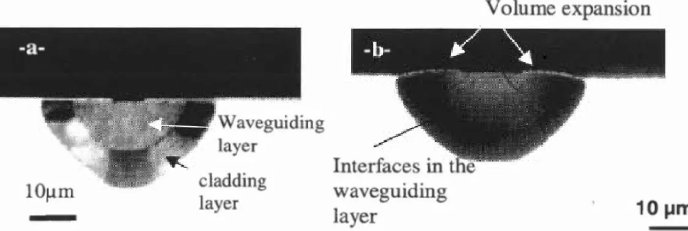
The geometry of the waveguides resembles that of a half cylinder (figure 1). A flat bottom is also observed and its size is dependent on the aperture mask. The thickness of each of the two layers constituting the waveguides is fixed by the anodisation time.
Two types of buried waveguides were fabricated in order to modify the propagation zone of light. The first type (samples A as-anodised and B oxidised) was realised with two-PS-Iayers by applying two constant current intensities. Nevertheless, the surface in contact with the electrolyte was not constant during the anodisation process and increased so that the density of current decreased as the porosity decreased. This resulted in an increase in the refractive index as illustrated in figure 2. In this case, the induced radial porosity gradient involves an opposite radial variation of waveguiding layer refractive index. Thus, its highest value is near the waveguiding layer/cladding layer interface.
Volume expansion
l Oum cladding
layer waveguiding 10
urn
layer
I -a-I J, I
,;:
I I I I ______________ ...1 _Intensity(u. a.)
-b-_,
~--I : n? I I Yo :..
11-:..
IlI-Waveguiding layér Cladding
I
! laver
Y
X (urn)
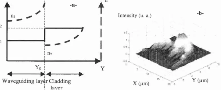
Figure 2 : a) Schematic representation of applied current intensity and refractive Index (samples Aand B);b) Near field profile for sample B.
Since the light will only propagate in the medium that has the highest refractive index, the propagation region will be near that of the interface. These waveguides have a non controled graded refractive index. Figure 2b illustrates the near field mode profiles of sample B. These experiments confirm the suspected variations in the refractive indexes with anodisation current and the localisation of the propagation region of light within the waveguide. A "flattened U" shape is obtained. The propagation zone is near the wageguiding/cladding interface.
The second type of sample, a step index buried waveguide (sample C), was realised by increasing the applied current intensity during the anodisation. Thus the current density is kept constant for each of the two layers of the waveguide as shown in figure 3a. A homogeneous near field profile is obtained inside the waveguiding layer (figure 3b).
-a- -b-Intensity (u.a.) Yo: Y I II1II
11-:..
II-Waveguiding] Cladding layer : layer I . I X (urn) Y(urn)Figure 3 : a) Schematic representation of applied current intensity and refractive Index (sample C);b) Near field profile for sample C.
The last type (sample D) is an intentionally graded index waveguide. The current density was kept relatively low at the initial time of PS formation and then increased as the PS grew. The increasing current density meant an increase in the porosity and so a decrease in the refractive index. The waveguiding layer index nïr) decreases with the radial distance from a maximum
value of n, at the air/waveguiding layer interface to reach a constant value n2 at the
waveguiding layer/cladding layer interface. The propagation region is suspected to be near the
air/waveguiding interface.
The measured optical losses (table 1) for the oxidised PS waveguides range from 3.75 dB/cm
to 9dB/cm which are much lower than that measured for unoxidised ones (22 dB/cm). In fact,
the PS absorption coefficient is more important than that of the oxidised PS. Nevertheless, this does not account for this important loss difference between oxidised and unoxidised PS waveguides.
For the sample A, the propagation region is near the waveguiding/cladding interface and the
optical losses are principally due to the roughness of this interface. The most important losses
of Band C samples would be due to the appearance of interfaces (figure 1-b) during the
formation of graded or step indexes by varying the current intensity. To reduce these losses a
ramp of current intensity should be applied with a shorter time in order to reduce the effects of
these interfaces with regard to the light wavelength.
Conclusion
The refractive index modulation is demonstrated. Step and graded index waveguides are
achieved. The propagation zone varies from air/waveguiding layer interface up to
waveguiding layer/cladding layer interface. Optical losses remain important but the major loss
mechanism is scattering due to the macro-roughness at different interfaces. It may possible to
minimise these losses by better controlling the applied intensity current with a shorter time. Lastly, a better understanding of the PS oxidation process also leads to a reduction in optical losses.
Acknowledgements
The authors are grateful to K. Mehadji and M. Thual from FranceTelecom for the near field
pattern measurements and the supplied micro lensed fibers.
References
[1] M. G. Berger, C. Dieker, M. Thônissen, L. Vescan, H. Lüth, H. Münder, W. Theiss, M.
Wernke, P. Grosse, J. Phys. D :Appl. Phys., 27, (1994) 1333.
[2] A Loni, L.T. Canham, M.G. Berger, R. Arens-Fischer, H. Munder, H. Luth, H.F. Arrand,
and T.M. Benson, Thin Solid Films, 276, (1996) 143.
[3] G. Maiello, S. LaMonica, A Ferrari, G. Masini, V.P. Bondarenko, AM. Dorofeev, and
N.M. Kazuchits, Thin Solid Films 297, (1997) 311.
[4] M. Araki, M. Takahashi, H. Koyama and N. Koshida, Mat. Res. Soc. Symp. Proc. Vol.
486, (1998) 107.
[5] A Halimaoui, «Porous silicon science and technology», ed J. C. Vial and J. Derrien