ÉCOLE DE TECHNOLOGIE SUPÉRIEURE UNIVERSITÉ DU QUÉBEC
THESIS PRESENTED TO
ÉCOLE DE TECHNOLOGIE SUPÉRIEURE
IN PARTIAL FULFILLMENT OF THE REQUIREMENTS FOR A MASTER'S DEGREE WITH THESIS IN ELECTRICAL ENGINEERING
M. A. Sc.
BY
Charles TRUDEAU
ELECTROSTATIC DEPOSITION OF GRAPHENE FOR USE IN PHOTO-CONDUCTIVE SWITCH
MONTREAL, OCTOBER 16, 2015
This Creative Commons licence allows readers to download this work and share it with others as long as the author is credited. The content of this work may not be modified in anyway or used commercially.
BOARD OF EXAMINERS (THESIS M.A.Sc.) THIS THESIS HAS BEEN EVALUATED BY THE FOLLOWING BOARD OF EXAMINERS
Prof. Sylvain G. Cloutier, Thesis Supervisor
Department of Electrical Engineering, École de technologie supérieure
Prof. Ricardo Zednik, Chair, Board of Examiners
Department of Mechanical Engineering, École de technologie supérieure
Mr. Martin Bolduc, External Evaluator INO (Institut National d'Optique)
THIS THESIS WAS PRENSENTED AND DEFENDED
IN THE PRESENCE OF A BOARD OF EXAMINERS AND THE PUBLIC OCTOBER 7, 2015
ACKNOWLEDGMENTS
This project would not have been possible if not for the help and guidance of many individuals. I will take the time to thank each of them personally. First of all I would like to thank my parents Alain Trudeau and Renee Gaulin for their continuous support and love in all matters of life but specifically for their support in my studies since I was a child, without them none of this would be possible. I would also like to thank my Thesis supervisor Sylvain G. Cloutier for his guidance in this project and his support when things did not go according to plan, I would also like to thank him for taking me in his research group, believing in me and my competence and providing an incredible work environment, it has been a pleasure to be under his supervision during my time at l'Ecole de Technologie Superieur. I would like to thank my good friend Cedric Sommers for his lifelong friendship and for introducing me to Sylvain Cloutier and his research. I will also take the time to thank each and every student in my research group since they all played a part even if not directly in this project. To Francois Xavier Fortier, I thank you for your technical advice, for your help with interfacing instruments and for our morning conversations over coffee. I would like to thank Xiaohang Guo for his light hearted attitude and our discussions on all matters. Debika Banerjee also played a part in the incredible working environment which I call our research group, I thank her for her sometimes jokester attitude which always lightens the mood in the office and also for her intelligent input in our technical discussions. I would like to thank Jaime Benavides for being a role model in terms of his hard working aptitude, for his expertise in chemical engineering and for our discussions on all matters of life. Felipe Gerlein became another role model of mine for his intelligence and relaxed attitude which is extremely welcome in times of stress, I thank him for this and for his help on anything relating to lasers and optics. Although Haythem Rehouma has not been with us for very long, I would like to thank him nonetheless for our morning conversations and for his input in technical discussions. Finally I would like to thank Nelson Landry, a research assistant to our research group, for all his help in any matter of instrumental set-up, design and fabrication. His help in matters of ordering parts and his connections to other laboratories and research personnel was also greatly appreciated, not to mention all his technical help on all matters.
ELECTROSTATIC DEPOSITION OF GRAPHENE FOR USE IN PHOTOCONDUCTIVE SWITCH
Charles TRUDEAU
ABSTRACT
Graphene, a material made up from a single atomic layer of honeycomb structured sp2 bonded carbon atoms, has been gaining interest in the last decade for its integration in optoelectronic devices in a wide range of fields. Many methods of graphene growth and deposition have been developed over the years. These methods range from high cost and high quality of deposited graphene to low cost and low quality of deposited graphene, depending on the applications wanted. An overview and comparison of these methods is presented in this work. More focus is placed on one such deposition method; the electrostatic deposition of graphene. This work aims to show the possibility to deposit micro graphene sheet arrays directly for the use in optoelectronic device active layers, such as bolometers and photoconductive switches. Improvements to the current technologies involving deposition of graphene using electrostatic forces have been investigated, more precisely, improvements to the control of the shape, size and position of the deposited graphene. These improvements are realised primarily via surface etching of the graphitic material used for deposition by pulsed UV Laser radiation. Etching of the graphitic material is performed to limit and therefore control the size of the deposited graphene. Patterning of the deposition substrate is also explored as a method of modifying local electric field strengths, moreover the possibility of direct deposition of graphene onto pattern SiO2 substrate to create suspended membranes is explored. However, deposition of graphene onto un-patterned SiO2 substrate are the main deposition results presented in this work. The optoelectronic properties of the deposited graphene were studied. More precisely, the deposited graphene is shown to have a direct electrical response to incident light of multiple wavelengths, thus making it suitable for photoconductive switch devices. The calorimetric properties of the deposited graphene were also studied, these results, however, were less conclusive, casting doubt on the effectiveness of graphene as a bolometer active layer. Improvements to the homogeneity of the cleaving process used in the electrostatic deposition of graphene were performed and are shown to lead to large scale graphene depositions, previously only thought to be achievable with more costly methods of graphene growth. A simple and accurate method of characterising the number of graphene layers present in the deposition is developed using the center of a single fitted gaussian curve on the 2D graphene Raman peak.
Keywords: Bolometer, Electrostatic Deposition, Graphene, Optoelectronics, Photoconductive switch, Raman Spectroscopy
DÉPÔT ÉLECTROSTATIQUE DE GRAPHÈNE POUR L'INTÉGRATION DANS DES INTERRUPTEURS PHOTOCONDUCTEURS
Charles TRUDEAU
RÉSUMÉ
Le graphène, un matériau constitué d'une seule couche atomique de carbone sp2 structurée en nid d'abeilles, attire beaucoup d'intérêt dans la dernière décennie pour son intégration dans des dispositifs optoélectroniques dans un large éventail de domaines. De nombreuses méthodes de croissance et dépôt de graphène ont été développés au fil des ans. Ces méthodes vont de coût élevé et de haute qualité du graphène déposé à des méthodes à faible coût et faible qualité du graphène déposé, selon les applications voulues. Une vue d'ensemble et une comparaison de ces méthodes est présentée dans ce travail. Un accent est mis sur un tel procédé de dépôt: le dépôt électrostatique de graphène. Ce travail vise à montrer la possibilité de déposer des matrices de feuille de graphène directement pour l'utilisation comme couches actives pour des dispositifs optoélectroniques tels que les interrupteurs photoconducteurs et les bolomètres. Des améliorations aux technologies actuelles impliquant le dépôt de graphène par force électrostatique sont présentées, plus précisément, sur le contrôle de la forme, la taille et la position de la déposition. Ces améliorations sur le contrôle du graphène déposé sont réalisées principalement par une gravure de la surface du matériau graphitique utilisé pour le dépôt par laser pulsé de rayonnement UV. La gravure du matériau graphitique est effectuée pour limiter et donc contrôler la taille du graphène déposé. Une gravure du substrat de déposition est également explorée comme un procédé de modification des intensités du champ électrique locale, outre la possibilité de dépôt direct du graphène sur un substrat de SiO2 engravé pour créer des membranes en suspension est exploré. Cependant, le dépôt de graphène sur un substrat de SiO2 non-modifié sont les principaux résultats de dépôt présentées dans ce travaille. Les propriétés optoélectroniques du graphène déposé ont été étudiés. Plus précisément, le graphène déposé a une réponse électrique directe à la lumière incidente de plusieurs longueurs d'onde, ce qui le rend convenable a l'utilisation pour des couches actives d'interrupteur photoconducteur. Les propriétés colorimétriques du graphène déposé ont également été étudiés, ces résultats, cependant, étaient moins concluants, jetant un doute sur l'efficacité du graphène comme couche active de bolomètres. Les améliorations apportées à l'homogénéité du processus de clivage utilisé dans le dépôt électrostatique du graphène peuvent conduire à des dépôts à grande échelle. Auparavant, les dépôts a grande échelle étaient uniquement réalisables avec des méthodes plus coûteuses de croissance de graphène. Un procédé simple et précis de la caractérisation du nombre de couches de graphène présents dans les dépôts a été mis au point. Cette méthode est réalisée à partir du centre d'une régression gaussienne sur la pic Raman 2D du graphène.
Mots-Clés: Bolomètre, Dépôt Électrostatique, Graphène, Interrupteur Photoconducteur, Optoélectronique, Spectroscopie Raman
TABLE OF CONTENTS
Page
INTRODUCTION ...1
CHAPTER 1 GRAPHENE FOR OPTOELECTRONIC DEVICES ...3
1.1 Graphene, wonder material? ...3
1.1.1 Electrical Properties and energy dispersion relations ... 3
1.1.2 Optical Properties ... 8
1.2 Bolometers ...12
1.2.1 A Theoretical Review Of Bolometers... 12
1.2.2 Current Bolometer Technologies ... 14
1.3 Photoconductive Switches ...15
1.3.1 A Theoretical Review Of Photoconductive Switches ... 16
1.3.2 Current Photoconductive Switch Technologies ... 17
1.4 Graphene Opto-Electronic Device Design ...19
CHAPTER 2 LITERATURE REVIEW OF GRAPHENE DEPOSITION AND CHARACTERISATION METHODS ...21
2.1 Literature Review: Graphene Deposition ...21
2.1.1 Chemical Vapour Deposition ... 21
2.1.1.1 General Theory of CVD ... 22
2.1.1.2 Methodology ... 23
2.1.1.3 Set-up and Materials ... 25
2.1.1.4 Transfer Process ... 26
2.1.1.5 Typical Results from CVD ... 28
2.1.2 Micro-Mechanical Deposition ... 31
2.1.2.1 Micro-Mechanical Deposition Theory ... 32
2.1.2.2 Methodology ... 33
2.1.2.3 Typical Results of Mirco-Mechanical Deposition ... 34
2.1.3 Electrostatic Deposition ... 36
2.1.3.1 Electrostatic Deposition Theory ... 37
2.1.3.2 Methodology and materials... 40
2.1.3.3 Typical Results from Electrostatic Deposition ... 42
2.1.4 Comparison of the different methods of deposition ... 44
2.2 Literature Review: Graphene Characterisation ...45
2.2.1 Methods of Layer Characterisation ... 46
2.2.1.1 AFM Thickness Measurements ... 46
2.2.1.2 SEM and Optical Characterisation ... 48
2.2.1.3 Raman Spectroscopy ... 49
CHAPTER 3 GRAPHENE PHOTOCONDUCTIVE SWITCH FABRICATION
USING ELECTROSTATIC DEPOSITION ...55
3.1 Methodology ...55
3.1.1 Set-up and Materials ... 56
3.1.2 Electrostatic Deposition with HOPG ... 60
3.1.2.1 Etching HOPG ... 60
3.1.2.2 SiO2 Substrate with Heat Sink Features ... 62
3.1.2.3 Optimising Deposition Parameters ... 65
3.1.2.4 HOPG Cleaving between deposition ... 68
3.2 Results of Electrostatic Deposition of Graphene ...70
3.2.1 Preliminary deposition ... 71
3.2.2 Deposition on pre-patterned substrate ... 73
3.2.3 Micro Sheet Deposition ... 74
3.2.4 Large Area Deposition ... 78
CHAPTER 4 GRAPHENE CHARACTERISATION ...81
4.1 Methodology ...81
4.1.1 Characterisation of the Number of Graphene Layers Deposited ... 81
4.1.2 Optoelectronic Measurements of Graphene ... 86
CONCLUSION ...92
LIST OF TABLES
Page Table 2.1 Transfer process of deposited graphene from a copper foil substrate to
final desired final substrate ...27 Table 3.1. Deposition voltages with resulting number of deposited graphene
layers for 20μm x 20μm etched islands onto SiO2 substrate in nitrogen atmosphere ...68 Table 4.1. 2D Raman peak evolution for increasing number of graphene layers.
Showing 2D peak center position and full width at half maximum ...85 Table 4.2. Electrostatically deposited graphene sheets separated into quality
LIST OF FIGURES
Page Figure 1.1 Energy dispersion of a) typical two-dimensional semiconductor and b)
of zero-bandgap graphene semiconductor. ...4 Figure 1.2 Monolayer graphene double resonance phonon relations. ...6 Figure 1.3 Bi-layered graphene double resonance phonon relations. ...7 Figure 1.4 Main graphene Raman spectrum features and associated phonon
relation processes. ...8 Figure 1.5 Transmittance for different transparent conductors: GTCFs39,
single-walled carbon nanotubes (SWNTs), ITO, ZnO/Ag/ZnO and
TiO2/Ag/TiO2. ...9 Figure 1.6 Transmittance for an increasing number of graphene layers. ...10 Figure 1.7 Non-linear optical properties of graphene and other carbon based
materials. ...11 Figure 1.8 Conceptual schematic of a bolometer device. Active layer absorbs
incident power P and heats up, ΔTemp = P/G. The active layer is
connected to a thermal reservoir through a thermal conductance G. ...13 Figure 1.9 Microbolometer, suspended membrane made from two thin metal
layers (absorber and thermistor). ...15 Figure 1.10 Sketch of photoconductive switch circuit design. ...16 Figure 1.11 Sketch of typical photoconductive response to incident light cycling. ...17 Figure 1.12 Schematic diagram and operation concept of photoconductive
terahertz emitters. ...18 Figure 1.13 Graphene bolometer/photoconductive switch design, showing active
layer graphene sheet, thermal reservoir and contacts. ...20 Figure 1.14 Graphene microbolometer/micro-photoconductive switch array design. ..20 Figure 2.1 Diagram showing CVD growth of graphene on copper substrate. ...24 Figure 2.2 Diagram of furnace set-up for CVD. ...25
Figure 2.3 Schematic showing the steps in the transfer process of CVD graphene
from a copper substrate to the desired substrate. ...27
Figure 2.4 Suspended graphene resonators. ...28
Figure 2.5 Optical microscope image of graphene on copper foil. ...29
Figure 2.6 SEM image of graphene domains on copper. ...30
Figure 2.7 Microscope image of SiO2 wafer after graphene transfer. ...31
Figure 2.8 Graphene shaving from HOPG block. ...32
Figure 2.9 Depositing graphene using vibrations. ...33
Figure 2.10 SEM image of the etched array of HOPG island. ...34
Figure 2.11 SEM image of HOPG islands of b) 200nm & c) 9μm in height. ...35
Figure 2.12 SEM image of deposited graphene sheets. ...35
Figure 2.13 AFM tapping mode image of deposited graphene sheet. ...36
Figure 2.14 Sketch of the interactions between the loosened graphene sheets and the deposition substrate. ...38
Figure 2.15 Electrostatic deposition of graphene from a bulk graphitic material to an insulating deposition substrate. ...39
Figure 2.16 Optical (a), SEM (b) and AFM (c) images of a graphene sheet produced by electrostatic transfer. A SEM image of the region depicted by the dashed box in (a) is shown in (b). The dashed box in (b) corresponds to the AFM image and the line scan shown in (c). ...43
Figure 2.17 Scanning tunnelling microscope images of (a) single (i) and double (ii) folded graphene. ...43
Figure 2.18 Height differences of the graphene (a) 1 day after deposition and (b) 45 days later after leaving it in a laboratory environment. The AFM height profiles (1)–(4) correspond to dashed lines (1)–(4), respectively, in (a) and (b). In either (a) or (b) the nearly square sheet on the left is 5 monolayers thick, while the large sheet on the right is 7 layers thick. ...47
Figure 2.19 Comparison of optical and SEM methods for determining the number of graphene layers on various substrates, (a) SiO2/Si, (b) mica, and (c) sapphire. ...48
Figure 2.20 a)SFM micrograph, b)FWHM of the D’ line, c)Raman mapping of the integrated intensity of the D line, d)integrated intensity of the G peak (solid line) and integrated intensity of the D line (dashed line), e) D peak for the edges (dashed for 2 to 1 layer, and solid for 1 to 0 layers). ...50 Figure 2.21 2D graphene Raman peak evolution. ...51 Figure 2.22 I-V curves of Graphene sample recorded by the iterative laser
switching on and off...52 Figure 2.23 I–V curves of Graphene Sample with and without 532nm illuminations. .53 Figure 2.24 A scatter plot of the ratio of the low (T ~ 100 mK) to room temperature
2-point resistance versus the room temperature 2-point resistance for all the devices for which there is low temperature data. (inset) Schematic of the device layout. ...54 Figure 3.1 Image of the top electrode set-up for electrostatic deposition of
graphene. ...57 Figure 3.2 Image of bottom copper electrode set-up for electrostatic deposition of
graphene. ...58 Figure 3.3 Electrostatic deposition set-up. ...58 Figure 3.4 Face view of the Stanford Research System Model PS375 +20kV 10W
used as the high voltage power supply for the electrostatic deposition of graphene. ...59 Figure 3.5 Labconco® Precise® Controlled Atmosphere Glove Box. ...59 Figure 3.6 HOPG etching depth of Samurai DPSS UV Laser Marking System...61 Figure 3.7 SiO2 Etching depth of Samurai DPSS UV Marking System for 50μm
features. ...63 Figure 3.8 3D optical image of 200μm trenches in SiO2 substrate etched with a
Samurai DPSS UV Marking System. All axis values are in μm. ...63 Figure 3.9 Top view of 50μm holes (red arrow) and artefacts (dashed orange
arrow) etched in SiO2 substrate with Samurai DPSS UV Marking
System. ...64 Figure 3.10 Optical image of electrostatic deposition of 700μm x700μm graphene
Figure 3.11 Homogeneous periodic loosening of underlying graphene sheet via
anchoring effect of HOPG island cleaving. ...70 Figure 3.12 Optical and Raman image of typical electrostatic deposition at 3.0kV
with un-patterned HOPG onto un-patterned SiO2 substrate. ...72 Figure 3.13 Optical and Raman image of typical electrostatic deposition at 5.0kV
with un-patterned HOPG onto un-patterned SiO2 substrate. ...72 Figure 3.14 SEM image of electrostatic deposition at 5kV with un-patterned HOPG
onto pre-patterned SiO2 substrate. ...73 Figure 3.15 Optical and Raman image of typical electrostatic deposition at 1.0kV
with un-patterned HOPG onto patterned SiO2 substrate. ...74 Figure 3.16 Optical and Raman image of typical electrostatic deposition at 3.0kV
with un-patterned HOPG onto patterned SiO2 substrate. ...74 Figure 3.17 Optical and Raman image of typical electrostatic deposition at 1.8kV
with patterned HOPG. ...75 Figure 3.18 Optical and Raman image of typical electrostatic deposition at 2.5kV
with patterned HOPG. ...75 Figure 3.19 1): Optical image of deposited arrays of micro graphene sheets. 2A) &
3A): optical image of single micro graphene sheets. 2B) & 3B): Raman image mapping 2D peak center position. Electrostatic deposition at 3.0kV with patterned HOPG. ...77 Figure 3.20 Optical and Raman image of typical electrostatic deposition at 4.0kV
with patterned HOPG. ...78 Figure 3.21 Optical and Raman image of typical electrostatic deposition at 5.0kV
with patterned HOPG. ...78 Figure 3.22 A) & B) Optical images of large scale single layer graphene deposition.
C) Raman image of same deposition showing spatially resolved 2D peak center position. ...79 Figure 4.1 SEM image from deposited graphene onto patterned SiO2. ...82 Figure 4.2 300R Alpha Raman microscope system from Witec with 532nm
excitation laser source. ...82 Figure 4.3 Optical and Raman image showing spatially resolved 2D Raman peak
center position of deposited graphene from un-patterned HOPG onto patterned SiO2 substrate. ...83
Figure 4.4 Evolution of 2D Raman peak with increasing number of graphene layers. Intensities in arbitrary units and shifted for easy viewing. Dashed line at 2700cm-1...84 Figure 4.5 Liquid Nitrogen constant flow Cryostat set-up with contacts on
graphene sample. ...86 Figure 4.6 Room temperature resistance of electrostatically deposited graphene
sheets. ...87 Figure 4.7 2-point temperature-dependent resistances of electrostatically deposited
graphene sheets. ...88 Figure 4.8 A scatter plot of the ratio of the low (T ~ -200°C) to room temperature
2-point resistance versus the room temperature 2-point resistance for all the devices for which there is low temperature data. ...89 Figure 4.9 I-V curves of electrostatically deposited graphene sheets as
photo-conductive switch excited with a Melles Griot 594nm 10mW laser. 10 minutes between readings. ...90 Figure 4.10 I-V curves of electrostatically deposited graphene sheets as
photo-conductive switch excited with a Santec tunable semiconductor TSL-200 laser set at 1540nm 0.7mW. 10 minutes between readings. ...91
LIST OF ABREVIATIONS
AFM Atomic Force Microscopy CVD Chemical Vapour Deposition DI Deionised
EM Electromagnetic waves
FWHM Full Width at Half Maximum HOPG Highly Ordered Pyrolytic Graphite
IPA Isopropyl Alcohol
IR Infra Red
I-V Current - Voltage Mins Minutes
MWNT Multi-Walled Nano-Tube
PMMA Poly(methyl methacrylate)
PVC Poly(vinyl chloride)
R_room Resistance at room temperature R_low Resistance at low temperature SEM Scanning Electron Microscopy SMU Source Measure Unit
SWNT Single-Walled Nano-Tube
TSL Tunnable Semiconductor Laser
UV Ultra Violet
LIST OF SYMBOLS AND UNITS OF MEASUREMENTS Electrical Units V volt kV kilovolt mA miliamp A amp Ω ohm kΩ kilo-ohm mW miliwatt W watt Geometric Units nm nanometer μm micrometer mm millimeter cm centimeter m meter " inches cm-1 wavenumber Ratio Symbols wt/wt weight ratio D/G D over G ratio % percentage Thermal Units °C degree Celsius mK mili-Kelvin K Kelvin Temporal Units s seconds mins minutes h hours GHz gigahertz MHz megahertz kHz kilohertz Hz hertz Weight Units g grams
INTRODUCTION
Graphene, a material made up from a single atomic layer of honeycomb structured sp2 bonded carbon atoms, has been gaining interest in the last decade since it was first separated from bulk graphite in 2004 (Hancock, 2011). The main interest from this material comes from its peculiar electronic properties as a zero bandgap semiconductor with a linear energy dispersion at the touching point of the conduction and valence bands. No other known materials exhibit such behaviours. Due to this unique dispersion relation, charge carriers within the graphene structure can be modelled as massless Dirac fermions (Hancock, 2011) (Bunch, 2008) (Sidorov et. al., 2007) compared with massive carriers found in materials which follow parabolic energy dispersions. This massless carrier model gives rise to unique transport properties found in no other material. This is why Andre Geim and Konstantin Noveselov received the 2010 Nobel Prize in Physics for the discovery and the "groundbreaking experiments regarding the two-dimensional material graphene"(Novoselov, K.S. et. al.,2004).
Graphene has been used and studied extensively in the last decade since it was first separated from bulk graphite by repeated cleaving of a graphite surface with household scotch tape (Geim, A.K., 2012). Since then, many research and development groups have been exploring the physical, optical and electric properties of single and few-layered graphene (Gilgueng et. al. 2009) (Gunasekaran & Kim, 2009) ( Beidaghi et. al. 2012). Some important phenomena observed by these groups, to name a few: the anomalous quantum Hall and Berry's phase effect (Fal'Ko, Vladimir I., 2008) high field degeneracy splitting (Zhang, Y. et. al., 2006), quantum confinement (Allen, M.T. et. al., 2012) and massless carrier transport properties (Chernozatonskii et. al., 2014) (Kliros, 2010). Many groups have also specialised in the production of graphene-like materials such as single-layered graphene, few-layered graphene and single- and multi-walled carbon-nanotubes (Guldi et. al. 2005) (Palser, 1999) (Kykamis et. al., 2005). As a result, there is now a multitude of methods of creating these materials. Some of these methods include the direct construction of graphene from gases (Pollard,
2011) and some deal with separating graphene from bulk graphitic materials (Sidorov, 2009), however all these methods have as an end goal to "deposit" graphene onto a substrate, these methods are therefore described as "graphene deposition methods". Many groups have also started to integrate graphene materials into functional devices such as photovoltaic devices (Kykamis et. al. 2002) (Camacho et. al., 2007) (Sgobba & Guldi, 2007), opto-electronic devices (Jianjun et. al., 2006), high frequency resonators (Van der Zande et. al., 2010), field effect transistors (Dharmendar et. al., 2011), etc.
In this work , single and few-layered graphene is shown to be able to be separated from bulk graphitic material and deposited via electrostatic forces. The size and position of the deposited graphene sheets is shown to be controllable to a certain degree and that these deposited sheets can be introduced as the active layer in optoelectronic devices. These graphene-based devices are shown to be sensitive to light sources and induce a measurable change in resistance. In chapter 1, a review of graphene properties and the theory behind these properties is put forward and explained. Also, an introduction to current optoelectronic device technologies, a theoretical review of these technologies and how graphene properties relate to these devices is included in this chapter. Chapter 2 deals with the many existing graphene deposition and characterisation methods, the reasoning behind the deposition method choice of this work and how it relates to optoelectronic device fabrication. Chapter 3 includes a detailed look at the experimental methodology of the electrostatic deposition of graphene onto patterned and un-patterned SiO2 substrates that is used in this work. This chapter also includes the results of the deposition experiments. Chapter 4 takes the deposition results found in the previous chapter and gives analytic details on the characterisation process of the resulting deposited graphene. The characterisation of the number of gaphene layer deposited and of the optoelectronic properties of the deposited graphene is performed in this chapter.
CHAPTER 1
GRAPHENE FOR OPTOELECTRONIC DEVICES
1.1 Graphene, wonder material?
Recent advances in the field of graphene deposition have led way to more advances in our understanding of the properties of this novel material. This crystalline zero bandgap semiconductor with linear energy dispersion offers many peculiar electrical properties such as massless charge carriers that are unique to graphene. These unique properties have prompted researchers in fields such as material science to consider graphene as a wonder material with almost unlimited applications. In this work, one such application: the use of graphene as the active layer in photoconductive switches and bolometer devices will be explored. The optoelectronic properties of these devices will be put to the test to help answer if graphene is really a wonder material. A theoretical review of the phonon and energy dispersion properties, the electrical properties and the optical properties of graphene follows in this chapter.
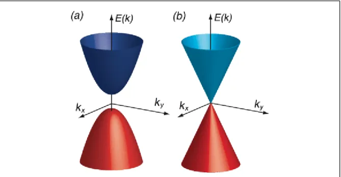
1.1.1 Electrical Properties and energy dispersion relations
The peculiar electronic properties of graphene originate from its unique energy dispersion. In this part of the chapter, the energy dispersion of monolayered graphene and that of bi-layered graphene is studied and its effect on the electrical properties and phonon relations are explained. Figure 1.1 shows the 2 dimensional energy dispersion relations of graphene, a zero-bandgap semiconductor compared to a typical semiconductor (Hatsugai, 2010). In this figure, the linear energy dispersion relation of graphene near the Dirac point is easily identifiable compared to the parabolic nature of the energy dispersion in typical semiconductors. The touching of the valance and conduction bands of graphene,which gives rise to the "zero-bandgap" designation, is also clearly visible.
Figure 1.1 Energy dispersion of a) typical two-dimensional semiconductor and b) of zero-bandgap graphene semiconductor
Taken from Hatasugai (2010)
The intrinsic properties of the energy dispersion relations of monolayered graphene have been shown to produce some unusual electrical properties. One such property, that has gained major interest in the recent years, is the linear energy dispersion relation of graphene. Such an energy dispersion relation gives rise to theoretically massless charged carriers and thus theoretically infinite carrier mobilities. From Newton's second law (assuming that acceleration is the rate of change in group velocity) and crystal momentum relations, the mass of charged carriers can be calculated, this is shown in equations 1.1 to 1.5. Equation 1.1 is Newton's second law, where F is the force vector, m∗ is the effective mass of the charged
carrier and a is the acceleration of said carriers. In equation 1.2, the acceleration is assumed to be equal to the rate of change in group velocity which is changed into reciprocal space, where ∇ is the del operator in reciprocal space and ( ) is the angular frequency. In equation 1.3, Newton's second law is applied to a crystal, where is the crystal momentum. Equation 1.4 combines equations 1.2 and 1.3 to give an expression of the acceleration in terms of E(k): the energy dispersion relation, ħ: the reduced Plank constant
and F: the force vector. Equation 1.5 combines equations 1.1 and 1.4 to give an expression for the effective mass in terms of ( ) ; the curvature of the energy dispersion relation.
=
∗ (1.1)=
=
(∇
( ))
= ∇
∇
( )
(1.2)=
= ħ
(1.3)= ∇
ħ
∇
( ) =
1
ħ
( )
=
1
ħ
( )
(1.4) ∗
= ħ
( )
(1.5)The curvature of a linear energy dispersion relation at the Dirac point is infinite and thus lead to an effective mass for the charged carriers of zero.
In practice, charge carrier mobilities in graphene have been measured to reach up to 15000cm2/Vs (Geim & Novoselov, 2007), this deviation from the theoretical value has been explained to be due to defects introduced in the non-perfect graphene formation process (Geim & Novoselov, 2007) and depends on the channel width and length of the device used for measurement.
Another interesting property of the energy dispersion relation in graphene is the double resonance process in monolayered and bilayered graphene. (Mallard et. al., 2009) This double resonance process helps to explain the 2D graphene Raman peak and the splitting of this peak with increased number of layers. The 2D Raman peak (~2700cm-1) found in graphene is due to two phonons with opposite momentum in the highest optical branch near the K point. The double resonance process links the phonon wave vectors to the electronic
band structure. This process for monolayered graphene is illustrated in figure 1.2. The Raman scattering process involving four virtual transitions: laser excitation of an electron-hole pair (vertical transition in figure 1.2), electron-phonon scattering with exchanged momentum q (horizontal transition in figure 1.2), electron-phonon scattering with negative exchanged momentum -q (horizontal transition in figure 1.2) and electron-hole recombination (vertical transition in figure 1.2). When the energy is conserved in these transitions, the double resonance conditions are met. The resulting 2D graphene Raman peak frequency is twice the frequency of the scattering phonon.
Figure 1.2 Monolayer graphene double resonance phonon relations
For bilayered graphene, the interactions of the graphene planes causes the π and π* bands to divide into four bands with a different splitting for electrons and holes (Zhenhua et. al., 2009) (Ferrari et. al., 2006), this is illustrated in figure 1.3. The 4 main resulting processes involve phonons with momenta q1B, q1A, q2A, and q2B, as shown in figure 1.3. There exists some other processes such as the four corresponding processes for the holes, and those associated to the 2 less intense optical transitions (not shown), these are associated to momenta almost identical to q1B, q1A, q2A, q2B and almost identical Raman shifts (Ferrari et. al., 2006). The main processes produce four different 2D sub-peaks in the Raman spectrum of bilayer
graphene. Similarly, further splitting of the 2D Raman peak occur with increased number of graphene layers (Ferrari et. al., 2006) (Mallard et. al., 2009). The Raman spectrum fingerprints for single-layer, bilayer, and few-layer graphene reveal changes in the electronic structure and electron-phonon interactions. This splitting in the 2D Raman peak of graphene allows for fast, unambiguous and nondestructive identification of graphene layers which will be explored in more detail further in this work.
Figure 1.3 Bi-layered graphene double resonance phonon relations
Other non resonant phonon relation processes within the graphene lattice give rise to other Raman peaks (Mallard et. al., 2009), these are summarised in figure 1.4 and shown along
with the main graphene Raman spectrum features. The other main Raman features found for graphene are the D peak and the G peak found at ~1350 cm-1 and ~1590 cm-1 respectively. The G peak is associated with the doubly degenerate iTO and LO phonon mode and the D peak is associated with a second-order process involving an iTO phonon and a defect within the graphene lattice.
Figure 1.4 Main graphene Raman spectrum features and associated phonon relation processes Adapted from Mallard et. al. (2009)
1.1.2 Optical Properties
Optical properties of graphene-based materials offer the potential for multiple diverse applications in optoelectronics. For example, induced graphene bandgap photoluminescence has been explored as an alternative to fluorescent quantum dots (Bonaccorso et.al., 2010), or the optical limiting found in graphene-based materials has been used in passive manipulation of optical beams and as high intensity laser pulse protection (Liu et. al., 2009). Following is a review of the absorption, emission and non-linear optical properties of graphene.
Graphene sheets exhibit very low optical absorption over a broad spectral range from the ultraviolet to the near-infrared. The optical transparency of graphene is very high, over 90%
from 300nm to 2500nm wavelength (Bonaccorso et.al., 2010). Similarly to other carbon-based materials, the π-plasmon absorption is the main factor in photon harvesting by graphene (Eberlein, et. al., 2008). Figures 1.5 and 1.6 show the wavelength dependent transmittance of single-layered graphene and the total visible transmittance of different number of graphene layers respectively. As can be seen from these figures a ~2.3% to 4% of light absorbance per graphene layer is measured for a wide range of wavelengths. A small increase in absorbance to ~10% is seen at in the ultraviolet range of the spectrum at ~275nm.
Figure 1.5 Transmittance for different transparent conductors: GTCFs39, single-walled carbon nanotubes (SWNTs), ITO, ZnO/Ag/ZnO and
TiO2/Ag/TiO2
Figure 1.6 Transmittance for an increasing number of graphene layers
Taken from Bonaccorso et. al. (2010)
Zero bangap pristine graphene offers no emission or luminescence mechanism apart from thermal blackbody radiation, only by introducing a bandgap can this be done. Chemical and physical treatments to pristine graphene can be employed to artificially introduce a bandgap in graphene by reducing the connectivity of the π-electron network (Bonaccorso et. al., 2010). Since the photoluminescence of such an altered connectivity of the π-electron network depends greatly upon the treatment applied (Bonaccorso et. al., 2010) and that no such treatment is performed in this work, the emission properties of altered graphene are not studied further.
The non-linear optical properties of graphene and graphene-based materials are by far the most interesting. One of these effects is the optical-limiting effect previously reported in graphene (Liu et. al., 2009). Optical limiter exhibit linear transmittance at low light intensities and reduced transmittance at high intensities. Broadband (450-1064 nm) optical-limiting properties have been observed in graphene sheets prepared from substoichiometric graphene-oxides (Dai et. al., 2015). However, this optical limiting has been related to the environment surrounding the graphene sheets rather than being an intrinsic property of the
absorbing domains in the sheets (Dai et. al., 2015). Figure 1.7 shows the optical-limiting effects of graphene-based materials (Liu et. al., 2009).
Figure 1.7 Non-linear optical properties of graphene and other carbon based materials Taken from Liu et. al. (2009)
1.2 Bolometers
Bolometers (sometimes called calorimeters) are devices which are able to measure the power of incident electromagnetic radiation via heating effects of a temperature-dependent conducting active layer. The word bolometer comes from the Greek words "bolometron" which translates roughly to "measurer of thrown things". Applications of bolometers are seen in a wide variety of fields spanning from dark matter detection in astronomy and particle physics (Gildemeister, 2000) to thermal imaging used in military grade night vision (Wood, 1993) and medical devices (Gorecki et. al., 2004). Bolometers can be used to measure incident radiation of most frequencies, however they are mostly used in infrared to terahertz radiation due to their high comparative sensitivity at these wavelengths (Richards, 1994). Outside of this range of frequencies there exists other devices which use different methods of detections that are more sensitive. In this part of the chapter, a review of the theory behind the method of light detection used in bolometers, the current bolometer technologies available and the proposed design of graphene based micro-bolometer devices is presented.
1.2.1 A Theoretical Review Of Bolometers
The following is a review of the principles of operation behind bolometer devices. Typically bolometer devices consist of an absorptive active layer connected to a thermal reservoir (Richards, 1994). Incident radiation comes into contact with the active layer of the bolometer which is then heated to temperatures above that of the thermal reservoir. This temperature change induces a change in resistivity in the temperature-dependent conducting active layer which can then be measured directly. Figure 1.8 shows a conceptual schematic of a bolometer device.
Figure 1.8 Conceptual schematic of a bolometer device. Active layer absorbs incident power P and heats up, ΔTemp = P/G. The active layer is connected to a thermal
reservoir through a thermal conductance G
With the known temperature-dependent resistivity of the active bolometer layer, the thermal conductance and thermal impedance between the active layer and the thermal reservoir, the electrical responsivity of the device can be calculated with equation 1.6
= = ( )
− ( )
Where S = electrical responsivity, I = bias current, = change in resistance with temperature, = thermal impedance, α(T) = temperature coefficient of resistance, G = thermal conductance, P = constant power of light source, V = bias voltage.
The response time or sampling frequency is an important property of any light sensitive devices, this is still true of bolometers. The response time of bolometer is based on the intrinsic thermal time constant which is equal to the ratio of the heat capacity of the active layer to the thermal conductance between it and the thermal reservoir. This is shown in equation 1.7.
= (1.7)
Where = intrinsic thermal time constant, C = heat capacity of active layer and G is the thermal conductance between the active layer and the thermal reservoir.
1.2.2 Current Bolometer Technologies
The first bolometer designs consisted generally of a metallic active layer operated at room temperature. These designs have evolved over time, the metallic active layer is now mainly replaced with semiconductors or superconductor absorptive materials and many devices are operated at cryogenic temperatures to improve their sensitivity and response time (Coron, 1976). The active layers of most current bolometer technologies are more often than not suspended membranes, a thermal reservoir is thus created from the spaces surrounding the suspended membranes (Yoneoka et. al., 2011).
Most of the current bolometer technologies use germanium-based materials, such as doped crystalline germanium and diamond-germanium composites, as their active layer (Draine et. al., 1976). Germanium-based materials generally offer good absorbance in the infrared part
of the spectrum, relatively high heat capacities and low thermal conductivity between it and the thermal reservoir. (Low, 1961) (Draine et. al., 1976)
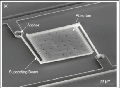
Recently, graphene is starting to gain interest as an active layer material in bolometers due to its particular electronic and transport properties (Hancock, 2011). Figure 1.9 shows the typical structure of a suspended microbolometer, this particular microbolometer's active layer is made up of two thin metal layers; an absorber and a thermistor.
Figure 1.9 Microbolometer, suspended membrane made from two thin metal layers (absorber and thermistor)
Taken from Yoneoka et. al. (2011) 1.3 Photoconductive Switches
Photoconductive switches are electrical switches which are based on the photoconductivity of an active material. This active material's electrical conductance increases as a function of incident light, much like a bolometer but without relying on heating effects. Generally photoconductive switches use semiconductors for the active layer, where light of energy greater than the semiconductor's bandgap is absorbed and generates free charge carriers. Since graphene is a zero bandgap semiconductor, it follows that there is no lower limit on the
photon energy capable of creating free charged carriers. Thus photoconductive switches that use graphene as an active layer should be sensitive to the whole electromagnetic spectrum.
1.3.1 A Theoretical Review Of Photoconductive Switches
As stated before, photoconductive switches rely on the photoconductivity properties of a semiconductor material. Photoconductivity is an opto-electronic phenomenon in which a material becomes more electrically conductive as a result of electromagnetic radiation absorption. When electromagnetic radiation of energy greater than the bandgap of said semiconductor is absorbed, the energy is enough to excite valence electrons to the conduction band thus increasing the number of free charge carriers and the overall electrical conductance of said semiconductor. If a voltage bias and a load resistor are added in series with a photoconductive material, a drop in voltage across the load resistor can be measured as an increase in current through the circuit is generated from the increase in electrical conductivity of the photoconductive material. A sketch of this basic photoconductive switch is presented in figure 1.10.
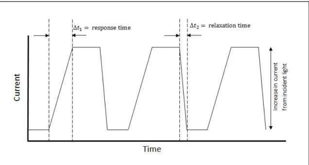
When photoconductive materials are subject to cycles of light illumination, the current passing through them can be measured directly, the "switching" behaviour becomes apparent. A sketch of a typical response to cycles of light illumination is shown in figure 1.11. From the incident light cycling response, the sampling frequency can be calculated from the measured response and relaxation time. This relation is shown in equation 1.8, where τ is the sampling frequency in hertz, ∆ is the response time in seconds and ∆ is the relaxation time also in seconds.
Figure 1.11 Sketch of typical photoconductive response to incident light cycling
= 1
∆ + ∆ ℎ
(1.8)
1.3.2 Current Photoconductive Switch Technologies
There exists different designs of photoconductive switches for different applications, all of these designs are generally of the metal-semiconductor-metal type. High voltage photoconductive switches are generally large devices, up to centimetres in length, with
electrical contacts on the end faces. For low power and high sampling frequencies, the devices are created with a small gap, a few microns in size, in a microstrip. For the highest sampling frequencies, sliding contact devices are created, where a point between the two parallel strips of a coplanar stripline is illuminated. These devices span a large range of applications, from generation of electrical terahertz pulses (Krokel et. al., 1989) (Smith et. al., 1989) to high-speed photodetectors in optical fiber communications (Kotaki et. al., 1987) and ultra-fast analog-to-digital converters (Miller, 2001). Figure 1.12 shows a schematic diagram and the operation concept of photoconductive terahertz emitters conceived by C.W. Berry and his team in 2013.
Figure 1.12 Schematic diagram and operation concept of photoconductive terahertz emitters
1.4 Graphene Optoelectronic Device Design
The aim of this work is to demonstrate an optoelectronic device such as a bolometer or a photoconductive switch using directly deposited graphene sheets as the active layer. The design behind such a device is similar to current technologies, which includes a suspended membrane as the active layer a thermal reservoir and contacts. By patterning "hole" features into the deposition substrate, it is possible to create thermal reservoirs which can then be covered by a deposited graphene sheet thus creating a suspended active layer membrane. Contacts can then be added and connected in a circuit with the other micro-devices in an array. Figure 1.13 illustrates the simple single photoconductive switch design, the choice of a base Si/SiO2 substrate comes from the availability and cost of such material but could be replaced by another material. This design is somewhat rudimentary, however it offers a basic stepping stone to further works on graphene-based bolometers and/or photoconductive switch. Figure 1.14 shows the design of the micro-devices acting as pixels as part of the whole array.
Figure 1.13 Graphene bolometer/photoconductive switch design, showing active layer graphene sheet, thermal reservoir and contacts
Figure 1.14 Graphene microbolometer/micro-photoconductive switch array design
CHAPTER 2
LITERATURE REVIEW OF GRAPHENE DEPOSITION AND
CHARACTERISATION METHODS
2.1 Literature Review: Graphene Deposition
Different methods of graphene deposition have been developed over time by researchers. These different methods of deposition each offer their advantages and drawbacks, some methods allow for deposition on any substrate while others only permit deposition on electrical insulators or metallic surfaces. Another parameter that depends on the method of deposition chosen is the amount of time needed for the deposition of graphene, this vary hugely from minutes to days. The cost of materials and apparatus needed for the deposition is another factor in choosing which method of deposition is ideal for certain projects. These methods also differ with regards to the size of the deposition area of graphene and the precision at which it can be deposited. It is important to note that the precision at which graphene can be deposited refers to both the spatial precision of deposition and also the precision of the number of graphene layer deposited. In the first parts of this chapter, the three most popular methods of graphene deposition will be analysed in detail, their advantages and drawbacks will be evaluated, and possible improvements of the methods will be discussed.
2.1.1 Chemical Vapour Deposition
Chemical vapour deposition or CVD has become one of if not the most popular deposition method for graphene (Hancock, 2011) (Pollard, 2011). Although it is called a deposition method, in CVD the graphene is more grown then deposited. This method of deposition is perhaps the most precise method of deposition, although the most strenuous method as it takes the longest time and is possibly the most expensive method to deposit graphene on a chosen substrate.
In this subsection, the CVD method of graphene deposition will be analysed in detail, a complete methodology of this deposition method will be explained, and conclusions will be drawn in relation to the project presented in this work.
2.1.1.1 General Theory of CVD
In the CVD process, carbon atoms are made to adhere to the surface of a metal substrate in a controlled environment (Pollard, 2011) (Obraztsov, 2009). Other carbon atoms then follow but are pushed to the sides of first atoms thus creating a one atom thick layer of carbon, this carbon layer is then crystallised into graphene by reducing the temperature of the controlled environment (Pollard, 2011)(Obraztsov, 2009). As the graphene grows from nucleation points in the lattice, eventually they will come into contact with the graphene grown from neighbouring nucleation points and thus will create boundaries between each region as their lattice orientation will inevitably differ (Pollard, 2011)(Yu, et. al., 2011). The growth of the graphene lattices will come to a stop when each region grown from nucleation points will be surrounded by the boundaries at which point they are called domains (Pollard, 2011)(Yu, et. al., 2011). The domain boundaries can be represented as defects in the complete graphene layer as the bond between the carbon atoms at such a boundary does not follow the Bravais lattice structure present in the bulk of the domains (Pollard, 2011)(Yu, et. al., 2011).
These defects are of great importance on the quality of the final graphene layer since they act as barriers for charge transport (Yu, et. al., 2011) and thus negatively affect the electrical properties of the graphene which have been discussed sub-chapter 1.1.1 of this work. Therefore, it is important to try and minimize the number of boundaries and to maximize the size of the domains.
2.1.1.2 Methodology
For CVD, a metal substrate such as copper is chosen as the deposition medium. Annealing the metal substrate is an important first step to increase the domain size of the deposited graphene. This is done by heating the metal in a furnace to around 1000°C under low vacuum (Pollard, 2011) (Obraztsov, 2009). For the deposition of the carbon atoms on the metal substrate, methane and hydrogen gases are flowed through the furnace while it is kept at the annealing temperature (Pollard, 2011) (Obraztsov, 2009). The hydrogen molecules catalyses a chemical reaction between the surface of the metal substrate and the methane molecules, resulting in the deposition of the carbon atom from the methane onto the surface of the substrate (Pollard, 2011). Due to this reaction with the surface of the substrate, the carbon atoms are deposited as a one atom thick layer on the surface (Pollard, 2011) (Yu, et. al., 2011). The diagram in figure 2.1 illustrates the deposition of carbon atoms onto a copper substrate. The furnace is then cooled rapidly to crystallise the carbon atoms into a contiguous graphene layer (Pollard, 2011) (Obraztsov, 2009). This rapid cooling also decreases the density of nucleation points and thus minimizes the defects due to domain boundaries (Pollard, 2011) (Yu, et. al., 2011). If the furnace is cooled too slowly, the layer of carbon can also aggregate into graphite (Pollard, 2011).
Figure 2.1 Diagram showing CVD growth of graphene on copper substrate
During the CVD process impurities can be introduced at many levels and can find their way into the final graphene layer. This introduction of impurities, be it from the substrate or the gases used in this method must be minimised or eliminated completely (Pollard, 2011) (Yu, et. al., 2011). Fortunately with experience, these impurities can be sufficiently minimised to create a graphene layer with a similar amount of impurities as exfoliated graphene flakes (Pollard, 2011). The difference between the thermal expansion between the graphene and the metal substrate can cause the graphene to wrinkle as it cools and crystallises (Kazi, et al., 2014). This effect can be minimised if proper annealing of the metal substrate is done (Kazi, et. al., 2014). Technically, this process of deposition can be used to create graphene sheets covering any sized substrate, however there are some limiting factors. One such factor is the size of furnaces available since the whole process needs to take place inside a furnace with a controlled environment (Pollard, 2011). Another limiting factor is the purity of the metal substrate used for the deposition since the metal needs to be perfectly smooth and devoid of defects to be able to create a single graphene sheet covering its entirety, these metal substrates can reach extremely high costs as their size increase.
(http://www.sigmaaldrich.com//materials-science/material-science-products.html?TablePage=108832768, visited August 2015)
2.1.1.3 Set-up and Materials
A simplified set-up of the apparatus needed to perform CVD is shown in figure 2.2. It includes a furnace and a quartz tube to provide the annealing for the metal substrate and the high temperatures needed for the process, a methane and a hydrogen gas line intake to the quartz tube to provide the gases needed for the deposition, an exhaust line to create the gas flow, a line to a vacuum pump to create the low vacuums needed for the metal substrate annealing and a crucible to hold the metal substrate inside the quartz tube and the furnace.
Figure 2.2 Diagram of furnace set-up for CVD
The flow rate of methane and hydrogen gas used in this method have an effect on the dynamics of the carbon deposition. An increase in methane provides more carbon atoms to be deposited and increases the number of nucleation points while an increase in hydrogen promotes the reaction between the methane and the surface of the metal substrate (Pollard, 2011).
Copper is only one of many metals that can be used as a deposition substrate, most transition metals can be used for such depositions. Other popular metals used in graphene CVD are cobalt and nickel (Pollard, 2011) (Kazi, et. al., 2014). Impurities and roughness of the substrate surface causes increases in the number of nucleation points and thus increases the defects due to graphene domain boundaries ( Yu, et. al., 2011).
2.1.1.4 Transfer Process
Once the graphene is deposited on the metal substrate it can then be transferred to any other desired substrate, this transfer process can be used to create suspended devices. Starting with the metal substrate covered on both sides with deposited graphene, one side is spin coated with an Anisole-PMMA solution to create a protective layer. The graphene is then etched off the other side of the metal substrate generally using oxygen plasma. The metal substrate and deposited graphene are then placed, PMMA face up, on the surface of an etchant solution (depending on the metal substrate choice) such as Ferric-Chloride for copper. Once the metal substrate is etched completely, the membrane is then removed from the etchant solution and scooped into DI water multiple times to clean it. With the desired final substrate, the membrane is scooped out of the DI water, the device is then left to dry. The Anisol-PMMA thin film is then removed by soaking the dried device into Dichloromethane until the thin film is completely removed. The device is then rinsed with acetone and IPA to clean it once more. If suspended devices are desired, care must be taken during the drying processes, critical point drying must be performed to get the device out of any liquid. Critical point drying must be performed to avoid any damage and movement that would occur to the suspended graphene from removing it from a liquid solution (Pollard, 2011) (van der Zande et. al., 2010). This typical transfer process from a copper foil substrate to a final desired substrate is summarized in Table 1 with illustrated steps in Figure 2.3.
Table 2.1 Transfer process of deposited graphene from a copper foil substrate to final desired final substrate
Steps Information
1 Copper with graphene deposited on both sides
2 Anisole-PMMA spin coated on one side to form protective layer 3 Etch graphene off PMMA-free side
4 Place copper-graphene-PMMA sample onto copper etchant solution 5 Let copper etch away completely
6 Scoop membrane and rinse in DI water
7 Scoop membrane out of DI water with desired final substrate 8 Let desired substrate and membrane dry
9 Remove PMMA with Dichloromethane solution 10 Rinse and clean with Acetone and IPA
Extra Critical point drying for suspended devices
Figure 2.3 Schematic showing the steps in the transfer process of CVD graphene from a copper substrate to the desired substrate
2.1.1.5 Typical Results from CVD
As described above, the CVD of graphene along with the transfer process makes the creation of suspended graphene devices possible. In the following part of the chapter typical devices that can be created with this method will be examined along with their quality.
Figure 2.4 Suspended graphene resonators Taken from van der Zande, et. al. (2010)
Figure 2.4 shows typical SEM images of suspended graphene ribbons over etched trenches, these were made by CVD of graphene onto copper and then transferred using critical point drying onto a pre-patterned silicon oxide substrate (van der Zande, et. al., 2010) . From Figure 2.4a) it can be seen that the graphene ribbons suspended over the 2um trenches show some deformation such as ripples (~10nm in amplitude) and some buckling of the ribbon (~100nm in amplitude) due to tension, shear and/or compression. The amount of deformations in this device varies between neighbouring suspended ribbons which signify that the tension, shear and compression in the graphene is somewhat variable. This variation is likely due to transfer process and/or the variable conditions of the CVD graphene prior to
the transfer. Moreover, for the longer suspended graphene ribbons, shown in Figure 2.4b), some large tears can be seen to occur in a few of the ribbons at mechanically weak grain boundaries inside the crystal matrix. Similar ripples and buckling to the short suspended graphene ribbons was also reported for the larger ribbons.
Figure 2.5 Optical microscope image of graphene on copper foil
Figure 2.6 SEM image of graphene domains on copper Taken from Pollard (2011)
Figure 2.5 shows an optical image of CVD graphene on a copper substrate (Pollard, 2011). It can be observed that the graphene is almost invisible, this is due to the graphene only absorbing ~2-4% of light per layer (Bonaccorso, et. al., 2010) and hence can barely be seen with the naked eye. Figure 2.6 shows an SEM image of the same CVD graphene on copper with a x10000 magnification to show the graphene domain boundaries (Pollar, 2011). The expected size of the graphene domains in CVD can vary extremely depending on many factors summarized in the sections above, these can range from less than a micron to a few hundred microns (Yu, et. al., 2011).
Figure 2.7 Microscope image of SiO2 wafer after graphene transfer Taken from Pollard (2011)
Figure 2.7 shows a large CVD graphene membrane transferred onto a silicon oxide wafer (Pollard, 2011). Some complications occur when transferring such a large graphene membrane, as can be seen from the figure, the graphene membrane crumpled on itself in some places. This most likely occurred while removing the PMMA from the graphene membrane in dichloromethane.
2.1.2 Micro-Mechanical Deposition
Another method for creating graphene sheets and depositing them is the micro-mechanical deposition method (Jayasena, et. al., 2013) (Chun-hu, et. al., 2012). This method makes use of mechanical forces to separate graphene from a block of bulk HOPG, the sheets can then be manipulated using an AFM tip. Micro-mechanical deposition of graphene is not a popular method of deposition but still offers some advantages over other methods. The reproducibility of the quality, shape and size of the deposited graphene is one of the main
advantages (Chun-hu, et. al., 2012). However the manipulation of graphene once it has been deposited can be rather difficult and time consuming (Jayasena, et. al., 2013).
2.1.2.1 Micro-Mechanical Deposition Theory
The theory behind micro-mechanical deposition is straightforward, using mechanical forces to brake off single layers of graphene from an HOPG block (Jayasena, et. al., 2013) (Chun-hu et. al., 2012) (Xuekun et. al., 1999). One of these methods involves shaving off graphene sheets from the top of an HOPG block (Jayasena, et. al., 2013), as shown in figure 2.8. Another method involves using vibration forces between the HOPG block and the deposition substrate to remove the top layers of graphene from the HOPG block (Xuekun et. al., 1999), as shown in figure 2.9. The deposited graphene sheets can later be moved with care using an AFM tip (Xuekun et. al., 1999).
Figure 2.9 Depositing graphene using vibrations.
2.1.2.2 Methodology
This chapter will focus on micro-mechanical deposition of graphene from a patterned HOPG substrate. The first step is to pattern the HOPG substrate, this can be done using oxygen plasma (Pollar, 2011) (Xuekun, et. al., 1999). The HOPG is first cleaved using a razor blade to create ~1.5mm thick pieces of HOPG, a thin film of SiO2 is then deposited using plasma enhanced chemical deposition (Xuekun, et. al., 1999). The SiO2 layer is then patterned to create a negative mask for the patterning of the HOPG (Xuekun, et. al., 1999). Oxygen plasma is then used to etch the HOPG to create island on the surface of the cleaved pieces (Xuekun, et. al., 1999). The thin film of SiO2 is then removed with dilute HF (Xuekun, et. al., 1999). From here the islands can be manipulated directly with an AFM tip or deposited using mechanical vibrations onto the preferred substrate (Xuekun, et. al., 1999) (Chun-un, et. al., 2012), as shown in figure 2.9. Again, using an AFM tip the deposited graphene can then be manipulated to fabricate devices or structures (Xuekun, et. al., 1999).
2.1.2.3 Typical Results of Mirco-Mechanical Deposition
For the aforementioned method, the size and shape of the deposited graphene is very constant, whereas the number of graphene layers deposited varies depending on the amount of vibration force that was applied during the deposition (Xuekun, et. al., 1999) . As shown in figure 2.10, the size and size of each etched HOPG island is constant and forms a uniform array.
Figure 2.10 SEM image of the etched array of HOPG island
Taken from Xuekun, et. al. (1999)
The height of such islands can be controlled by controlling the parameters of the oxygen plasma etching (Xuekun, et. al., 1999). Figure 2.11 shows two different heights of HOPG island (b = 200nm & c = 9μm). The 200nm islands were found to be a good height for manipulation with an AFM tip (Xuekun, et. al., 1999). As can be seen from this image, the thicker islands have a larger base then tip size, this is due to the oxygen plasma etching (Xuekun, et. al., 1999).
Figure 2.11 SEM image of HOPG islands of b) 200nm & c) 9μm in height
Taken from Xuekun, et. al. (1999)
Figure 2.12 shows the results of the deposition process for 6 μm thick island (Xuekun, et. al., 1999). The size of each graphene sheet is rather constant, however some of the deposited graphene stayed in stacks (Figure 2.12a) while others were found to be fanned out into thinner sheets (Figure 2.12b) (Xuekun, et. al., 1999). Very thin layers of graphene up to single layers, where observed to be deposited in the fanned out depositions compared to the stacked depositions (Xuekun, et. al., 1999). The thinnest sheets of graphene deposited using this method were found in the more fanned out deposition which were observed to occur with increased "rubbing" between the HOPG and the SiO2 (Xuekun, et. al., 1999).
Figure 2.12 SEM image of deposited graphene sheets Taken from Xuekun, et. al. (1999)
Figure 2.13 AFM tapping mode image of deposited graphene sheet
Taken from Xuekun, et. al. (1999)
Figure 2.13 shows the height profile of one such deposited graphene sheet using AFM tapping mode. The graphene sheet deposited in this image is rather thick (up to ~100nm) thus is in the order of 100 atomic layers, with some of the layers folding back on themselves (Xuekun, et. al., 1999).
2.1.3 Electrostatic Deposition
The electrostatic deposition of graphene, much like the micro-mechanical deposition method, is another method of removing graphene from a bulk graphitic material to a desired substrate (Sidorov, et. al., 2007) (Sidorov, 2009). This method of deposition makes use of electrical charges and fields to separate the gaphene and deposit it directly on the wanted substrate (Sidorov, 2009). This technique is not as popular as other techniques of graphene deposition since the size and quality of the deposited graphene is not as easily controllable as the other methods, especially the CVD method with better spatial selectivity (Sidorov, 2009) (Pollard 2011). Although this method has some drawbacks it is not without advantages, the electrostatic deposition of graphene offers what is probably the cheapest and fastest way to
deposit graphene (Sidorov, 2009) (Geim, 2012). As an emerging technique, it also offers room for improving the technique to minimize any of the drawbacks associated with this method of deposition.
2.1.3.1 Electrostatic Deposition Theory
Electrostatic deposition of graphene uses electrical charges and fields to separate already loosened graphene from a bulk graphitic material such as HOPG (Sidorov, 2009). By applying a large electrical potential between two electrodes supporting a bulk graphitic material and an insulating deposition substrate, a large electrical field can be generated. The loose graphene sheets on the surface of the bulk graphitic material opposing the electrode becomes charged due to the applied electrical potential (Sidorov, et. al., 2007) (Sidorov, 2009). By bringing the bulk graphitic material with the charged loose graphene sheets into contact with the insulating deposition substrate, the charged loose graphene sheets separate from the bulk graphitic material due to the increased electrical field applying a force greater than the force of adhesion between the bulk graphitic material and the loose graphene sheets (Sidorov, 2009). A sketch of the interaction between the loosened graphene sheets and the deposition substrate is illustrated in figure 2.14. The separated charged graphene sheets are attracted to the grounded electrode and then adhere to the insulating deposition substrate, and thus are deposited. This process is shown in figure 2.15.
Figure 2.14 Sketch of the interactions between the loosened graphene sheets and the deposition substrate
Figure 2.15 Electrostatic deposition of graphene from a bulk graphitic material to an insulating deposition substrate
Some of the limiting factors of this method can be seen straight away, one such limiting factor is the fact that the deposition substrate needs to be insulated from the grounded electrode otherwise the electrical field will vanish when the bulk graphitic material is brought into contact with the deposition substrate (Sidorov, 2009). If the wanted deposition substrate