HAL Id: tel-00908579
https://tel.archives-ouvertes.fr/tel-00908579
Submitted on 25 Nov 2013HAL is a multi-disciplinary open access archive for the deposit and dissemination of sci-entific research documents, whether they are pub-lished or not. The documents may come from teaching and research institutions in France or abroad, or from public or private research centers.
L’archive ouverte pluridisciplinaire HAL, est destinée au dépôt et à la diffusion de documents scientifiques de niveau recherche, publiés ou non, émanant des établissements d’enseignement et de recherche français ou étrangers, des laboratoires publics ou privés.
Throughput Oriented Analytical Models for
Performance Estimation on Programmable Accelerators
Junjie Lai
To cite this version:
Junjie Lai. Throughput Oriented Analytical Models for Performance Estimation on Programmable Accelerators. Hardware Architecture [cs.AR]. Université de Rennes I, 2013. English. �tel-00908579�
TH `
ESE / UNIVERSIT ´
E DE RENNES 1
sous le sceau de l’Universit ´e Europ ´eenne de Bretagne
pour le grade de
DOCTEUR DE L’UNIVERSIT ´
E DE RENNES 1
Mention : Informatique
´
Ecole doctorale Matisse
pr ´esent ´ee par
Junjie L
AI
pr ´epar ´ee `a l’unit ´e de recherche INRIA – Bretagne Atlantique
Institut National de Recherche en Informatique et Automatique
Composante Universitaire (ISTIC)
Throughput-Oriented
Analytical Models for
Performance
Estima-tion on Programmable
Hardware Accelerators
Th `ese sera soutenue `a Rennes le 15 F ´evrier 2013
devant le jury compos ´e de :
Denis Barthou
Professeur, Universit ´e de Bordeaux/Rapporteur
Bernard Goossens
Professeur, Universit ´e de Perpignan/Rapporteur
Gilbert Grosdidier
Directeur de Recherches CNRS, LAL, Orsay /
Examinateur
Dominique Lavenier
Directeur de Recherches CNRS, IRISA, Rennes /
Examinateur
Isabelle Puaut
Professeur Universit ´e de Rennes I/Examinatrice
Amirali Banisiadi
Professor University of Victoria, Canada/Examinateur
Andr ´e Seznec
Directeur de Recherches INRIA, IRISA/INRIA Rennes /
I want to thank my colleagues and also friends of the current and previous team members, who make my 3-years’ work in the ALF team a very pleasant experience.
I want to thank my wife and my parents for their constant support in my life.
Contents 6
R´esum´e en Fran¸cais 8
Introduction 19
1 Performance Analysis of GPU applications 23
1.1 GPU Architecture and CUDA Programming Model . . . 23
1.1.1 GPU Processor . . . 23
1.1.2 Comparison of Recent Generations of NVIDIA GPUs . . . 24
1.1.3 CUDA Programming Model . . . 26
1.2 Performance Prediction of GPU Applications Using Simulation Approach . . . 28
1.2.1 Baseline Architecture . . . 28
1.2.2 Simulation Flow . . . 29
1.2.3 Accuracy . . . 29
1.2.4 Limitations . . . 30
1.3 Performance Projection/Prediction of GPU Applications Using Analytical Per-formance Models . . . 30
1.3.1 MWP-CWP Model . . . 31
1.3.1.1 Limitations . . . 32
1.3.2 Extended MWP-CWP Model . . . 33
1.3.2.1 Limitations . . . 34
1.3.3 A Quantitative Performance Analysis Model . . . 34
1.3.3.1 Limitations . . . 36
1.3.4 GPU Performance Projection from CPU Code Skeletons . . . 36
1.3.4.1 Limitations . . . 37
1.3.5 Summary for Analytical Approaches . . . 37
1.4 Performance Optimization Space Exploration for CUDA Applications . . . 38
1.4.1 Program Optimization Space Pruning . . . 39
1.4.2 Roofline Model . . . 40
1.4.3 Summary . . . 40
2 Data-flow Models of Lattice QCD on Cell B.E. and GPGPU 43 2.1 Introduction . . . 43
2.2 Analytical Data-flow Models for Cell B.E. and GPGPU . . . 44
Contents 7
2.2.1 Cell Processor Analytical Model . . . 44
2.2.2 GPU Analytical Model . . . 47
2.2.3 Comparison of Two Analytical Models . . . 48
2.3 Analysis of the Lattice-QCD Hopping Matrix Routine . . . 49
2.4 Performance Analysis . . . 51
2.4.1 Memory Access Patterns Analysis . . . 52
2.4.1.1 Cell Performance Analysis . . . 54
2.4.2 GPU Performance Analysis . . . 55
2.5 Summary . . . 55
3 Performance Estimation of GPU Applications Using an Analytical Method 57 3.1 Introduction . . . 57
3.2 Model Setup . . . 58
3.2.1 GPU Analytical Model . . . 58
3.2.2 Model Parameters . . . 59
3.2.2.1 Instruction Latency . . . 60
Execution latency . . . 60
Multiple-warp issue latency . . . 61
Same-warp issue latency . . . 61
3.2.2.2 Performance Scaling on One SM . . . 62
3.2.2.3 Masked instruction . . . 62
3.2.2.4 Memory Access . . . 63
3.2.3 Performance Effects . . . 63
3.2.3.1 Branch Divergence . . . 63
3.2.3.2 Instruction Dependence and Memory Access Latency . . . . 63
3.2.3.3 Bank Conflicts in Shared Memory . . . 64
3.2.3.4 Uncoalesced Memory Access in Global Memory . . . 64
3.2.3.5 Chanel Skew in Global Memory . . . 64
3.3 Workflow of TEG . . . 64
3.4 Evaluation . . . 66
3.4.1 Dense Matrix Multiplication . . . 66
3.4.2 Lattice QCD . . . 68
3.5 Performance Scaling Analysis . . . 70
3.6 Summary . . . 74
4 Performance Upper Bound Analysis and Optimization of SGEMM on Fermi and Kepler GPUs 77 4.1 Introduction . . . 77
4.2 CUDA Programming with Native Assembly Code . . . 79
4.2.1 Using Native Assembly Code in CUDA Runtime API Source Code . . 79
4.2.2 Kepler GPU Binary File Format . . . 81
4.2.3 Math Instruction Throughput on Kepler GPU . . . 81
4.3.1 Using Wider Load Instructions . . . 85
4.3.2 Register Blocking . . . 86
4.3.3 Active Threads on SM . . . 87
4.3.4 Register and Shared Memory Blocking Factors . . . 88
4.3.5 Potential Peak Performance of SGEMM . . . 89
4.4 Assembly Code Level Optimization . . . 91
4.4.1 Optimization of Memory Accesses . . . 91
4.4.2 Register Spilling Elimination . . . 92
4.4.3 Instruction Reordering . . . 93
4.4.4 Register Allocation for Kepler GPU . . . 93
4.4.5 Opportunity for Automatic Tools . . . 95
4.5 Summary . . . 96
Conclusion 101
Bibliography 111
9
Résumé en Français
L'ère du multi-cœur est arrivée. Les fournisseurs continuent d'ajouter des cœurs aux puces et avec davantage de cœurs, les consommateurs sont persuadés de transformer leurs ordinateurs en plateformes. Cependant, très peu d'applications sont optimisées pour les systèmes multi-cœurs. Il reste difficile de développer efficacement et de façon rentable des applications parallèles. Ces dernières années, de plus en plus de chercheurs dans le domaine de la HPS ont commencé à utiliser les GPU (Graphics Processing Unit, unité de traitement graphique) pour accélérer les applications parallèles. Une GPU est composée de nombreux cœurs plus petits et plus simples que les processeurs de CPU multi-cœurs des ordinateurs de bureau. Il n'est pas difficile d'adapter une application en série à une plateforme GPU. Bien que peu d'efforts soient nécessaires pour adapter de manière fonctionnelle les applications aux GPU, les programmeurs doivent encore passer beaucoup de temps à optimiser leurs applications pour de meilleures performances.
Afin de mieux comprendre le résultat des performances et de mieux optimiser les applications de GPU, la communauté GPGPU travaille sur plusieurs thématiques intéressantes. Des modèles de performance analytique sont créés pour aider les développeurs à comprendre le résultat de performance et localiser le goulot d'étranglement. Certains outils de réglage automatique sont conçus pour transformer le modèle d'accès aux données, l'agencement du code, ou explorer automatiquement l'espace de conception. Quelques simulateurs pour applications de GPU sont également lancés. La difficulté évidente pour l'analyse de performance des applications de GPGPU réside dans le fait que l'architecture sous-jacente de la GPU est très peu documentée. La plupart des approches développées jusqu'à présent n'étant pas assez bonnes pour une optimisation efficace des applications du monde réel, et l'architecture des GPU évoluant très rapidement, la communauté a encore besoin de perfectionner les modèles et de développer de nouvelles approches qui permettront aux développeurs de mieux optimiser les applications de GPU.
Dans ce travail de thèse, nous avons principalement travaillé sur deux aspects de l'analyse de performance des GPU. En premier lieu, nous avons étudié comment mieux estimer les performances des GPU à travers une approche analytique. Nous souhaitons élaborer une approche suffisamment simple pour être utilisée par les développeurs, et permettant de mieux visualiser les résultats de performance. En second lieu, nous tentons d'élaborer une approche permettant d'estimer la limite de performance supérieure d'une application dans certaines architectures de GPU, et d'orienter l'optimisation des performances.
10
architectures GPGPU GT200 et Cell B.E. La section 3 présente notre travail sur l'estimation de performance à l'aide d'une approche analytique, qui a fait partie du séminaire de travail Rapido 2012. La section 4 présente notre travail sur l'analyse de la limite de performance supérieure des applications de GPU ; il fera partie du CGO 2013. La section 5 conclut cette thèse et fournit des orientations pour le futur.
1
Modèle de flux de données de QCD sur réseau sur Cell
B.E. et GPGPU
La chromodynamique quantique (QCD pour Quantum chromodynamics) est la théorie physique des interactions entre les éléments fondamentaux de la matière, et la QCD sur réseau est une approche numérique systématique pour l'étude de la théorie de la QCD. L'objectif de cette partie du travail de thèse est de fournir des modèles de performance analytique de l'algorithme de QCD sur réseau sur architecture multi-cœur. Deux architectures, les processeurs GPGPU GT200 et CELL B.E., sont étudiées et les abstractions matérielles sont proposées.
2.1 Comparaison de deux modèles analytiques
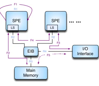
La Figure 1 offre une comparaison des deux modèles présentés. Les principales différences entre les deux plateformes de mise en œuvre de la QCD sur réseau sont les différences de hiérarchie de mémoire et de modèle d'interconnexion des différentes unités de processeurs, qui auront une influence sur le modèle d'accès à la mémoire. Le modèle d'accès à la mémoire est la clé des exigences en termes de flux de données, et donc, la clé de la performance.
2.2 Routine de QCD sur réseau Hopping_Matrix
Hopping_Matrix est la routine la plus longue de l'algorithme de QCD sur réseau : elle occupe environ 90 % du temps d'exécution total. Les structures de données d'entrée de la routine Hopping_Matrix incluent le champ de spineur, le champ de jauge,
11
Figure 1 : comparaison des modèles analytiques de Cell et GPU
le résultat est le champ de spineur obtenu. Les données temporaires correspondent au champ du demi-spineur intermédiaire.
2.3 Analyse de performance
Notre méthodologie consiste à obtenir la performance potentielle sur la base de l'analyse du flux de données. Avec des modèles de processeurs et l'application, les modèles d'accès à la mémoire sont résumés, ce qui permet ensuite de générer les informations relatives au flux de données. Il est ensuite possible d'estimer les exigences des données en termes de bande passante sur la base des informations relatives au flux de données. En identifiant le composant du goulot d'étranglement, la performance potentielle de l'application est calculée par l'intermédiaire de la bande passante maximale du composant.
En utilisant les modèles analytiques présentés, on catégorise les modèles d'accès à la mémoire comme indiqué dans le Tableau 1.
Dans une mise en œuvre, tous les modèles peuvent ne pas être appliqués simultanément, en raison des contraintes de ressources du processeur. Pour différentes mises en œuvre, de nombreuses combinaisons de ces modèles sont donc applicables. Pour obtenir des performances optimales sur une architecture spécifique, il est possible de sélectionner la meilleure combinaison en fonction des caractéristiques de l'architecture.
Pour un processeur Cell B.E., la base locale peut contenir les données de champ d'un sous-réseau avec suffisamment de sites d'espace-temps. Les modèles P2 et P3 pourraient donc être appliqués. Le SPE pouvant émettre directement des opérations I/O, les données de champ du demi-spineur de limite peuvent être directement transférées sans être réécrites dans la mémoire principale. Le modèle P4 est donc réalisable. Différents SPE pouvant communiquer directement à travers l'EIB, le modèle P5 est également réalisable. La combinaison optimale pour le processeur Cell est (01111). Avec la combinaison de modèle (01111), la performance de pointe potentielle pour
SIMD SIMD SIMT SIMT
I/O Mémoire principale Mémoire graphique I/O LS LS Partage RF Partage RF
12
P1 Reconstitution du champ de jauge dans le processeur
P 2 Partage total des données du champ de jauge entre les sites
d'espace-temps voisins
P 3
Les données de champ du demi-spineur intermédiaire sont contenues dans la mémoire rapide locale, sans nécessiter de réécriture dans la mémoire principale
P 4
Les données de champ du demi-spineur de limite inter processeurs sont stockées dans la mémoire rapide locale, sans nécessiter de réécriture dans la mémoire principale
P 5
Les données de champ du demi-spineur de limite inter-cœurs sont stockées dans la mémoire rapide locale, sans nécessiter de réécriture dans la mémoire principale
Tableau 1 : modèle d'accès à la mémoire
DSlash est d'environ 35 GFlops (34 % de la performance de pointe théorique de Cell, avec 102,4 GFlops).
Pour la GPU GT200, il est impossible de stocker l'ensemble des données de champ de demi-spineur intermédiaire. La GPU n'étant pas capable d'émettre directement les opérations I/O, le modèle P4 est impossible. Il n'y a pas de communication directe entre cœurs dans le GPU. P5 est donc également irréalisable. Chaque GPU ayant une grande puissance de calcul, il est envisageable de reconstruire les données de champ de jauge à l'intérieur du processeur. La combinaison de modèle possible pourrait donc être (10000). Avec la combinaison de modèle (10000), si l'on tient uniquement compte d'un nœud de GPU simple, la performance potentielle est de 75,6 GFlops, soit environ 65 % de la performance de pointe théorique en double précision.
2
Estimation de performance des applications de GPU à
travers l'utilisation d'une méthode analytique
L'objectif de la deuxième partie de ce travail de thèse est de fournir une approche analytique permettant de mieux comprendre les résultats de performance des GPU. Nous avons développé un modèle de temporisation pour la GPU NVIDIA GT200 et construit l'outil TEG (Timing Estimation tool for GPU) sur la base de ce modèle. TEG prend pour éléments de départ le code assembleur de noyau CUDA et le suivi des instructions. Le code binaire du noyau CUDA est désassemblé à l'aide de l'outil cuobjdump fourni par NVIDIA. Le suivi des instructions est obtenu grâce au simulateur Barra. Ensuite, TEG modélise l'exécution du noyau sur la GPU et collecte les informations de temporisation. Les cas évalués montrent que TEG peut obtenir une approximation de performance très proche. En comparaison avec le
13
approximation. En comparaison avec le nombre réel de cycles d'exécution, TEG présente généralement un taux d'erreur inférieur à 10 %.
3.1 Paramètres du modèle
Pour utiliser le modèle analytique dans TEG, il faut définir des paramètres du modèle. Cette section présente certains des principaux paramètres.
La latence d'exécution d'une instruction de chaîne désigne les cycles au cours desquels l'instruction est active dans l'unité fonctionnelle correspondante. Après la latence d'exécution, une instruction de chaîne émise est marquée comme terminée.
La latence d'émission de la même chaîne d'une instruction correspond aux cycles au cours desquels le moteur d'émission doit attendre avant d'émettre une autre instruction, après avoir émis une instruction de chaîne. Elle est calculée à l'aide du débit d'instruction.
La latence d'émission de la même chaîne correspond aux cycles au cours desquels le moteur d'émission doit attendre avant d'émettre une autre instruction issue de la même chaîne, après avoir émis une instruction de chaîne. Cette latence peut également être mesurée à l'aide de la fonction d'horloge() ; elle est généralement plus longue que la latence d'émission de plusieurs chaînes.
3.2 Évaluation
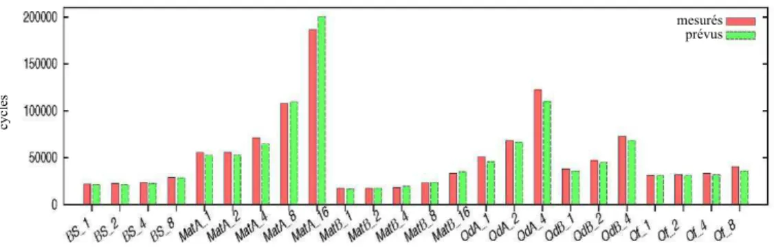
Figure 2 : analyse des erreurs de TEG
Nous évaluons TEG à l'aide de plusieurs repères selon différentes configurations et comparons les temps d'exécution mesurés et estimés du noyau. Le résultat est présenté dans la Figure 2. Le nom est défini ainsi :
NomDeNoyau-NombreDeChaînes. BS, MatA, MatB, QdA, QdB, Qf correspondent respectivement
à Blackscholes, multiplication naïve de matrice, multiplication de matrice sans conflit de banque de mémoire partagée, noyau
Analyse des erreurs d'estimation de performance à l'aide de TEG
mesurés prévus
cy
cl
14
QCD sur réseau en double précision avec accès mémoire non coalescé, noyau QCD sur réseau en double précision avec accès mémoire coalescé, et noyau QCD sur réseau en simple précision. NombreDeChaînes est le nombre de chaînes concomitantes attribuées à chaque SM. Ici, la même charge est attribuée à toutes les chaînes. Le résultat indique que TEG présente une bonne approximation et qu'il peut également déceler le comportement de mise à l'échelle des performances. Le taux moyen d'erreur absolue relative est de 5,09 % et le taux maximum d'erreur absolue relative est de 11,94 %.
3
Analyse de la limite de performance supérieure et
optimisation de SGEMM sur les GPU Fermi et Kepler
Pour comprendre les résultats de performance des GPU, il existe de nombreux travaux traitant de la façon de prévoir/prédire la performance des applications CUDA à travers des méthodes analytiques. Toutefois, les modèles de performance des GPU reposent tous sur un certain niveau de mise en œuvre de l'application (code C++, code PTX, code assembleur...) et ne répondent pas à la question de la qualité de la version optimisée actuelle, et de l'utilité d'un éventuel effort d'optimisation supplémentaire. Différente des modèles de performance des GPU existants, notre approche ne prévoit pas la performance possible en fonction de certaines mises en œuvre, mais la limite de performance supérieure qu'une application ne peut dépasser.
4.1 Approche d'analyse générale pour la performance de pointe potentielle
L'approche d'analyse générale peut être la même pour toutes les applications, mais le processus d'analyse détaillée peut varier d'une application à l'autre.
En premier lieu, nous devons analyser les types d'instructions et le pourcentage d'une routine. En second lieu, nous devons trouver quels paramètres critiques ont un impact sur le pourcentage de mélange des instructions. Troisièmement, nous analysons de quelle manière le débit d'instruction varie en fonction de la modification de ces paramètres critiques. Quatrièmement, nous pouvons utiliser le débit d'instructions et la combinaison optimale des paramètres critiques pour estimer la limite de performance supérieure. Avec cette approche, nous pouvons non seulement obtenir une estimation de la limite de performance supérieure, connaître l'écart de performance restant et déterminer l'effort d'optimisation, mais aussi comprendre quels paramètres sont essentiels à la performance et comment répartir notre effort d'optimisation.
15
4.2 Analyse de la performance de pointe potentielle pour SGEMM
Pour SGEMM, tous les noyaux SGEMM correctement mis en œuvre utilisent la mémoire partagée de la GPU pour diminuer la pression exercée sur la mémoire globale. Les données sont d'abord chargées depuis la mémoire globale vers la mémoire partagée, puis les threads d'un même bloc peuvent partager les données chargées dans la mémoire partagée. Pour les GPU Fermi (GF110) et Kepler (GK104), des instructions arithmétiques telles que FFMA ne peuvent pas accepter d'opérandes en provenance de la mémoire partagée. Les instructions LDS étant nécessaires au chargement des données initial depuis la mémoire partagée vers les registres, la plupart des instructions exécutées en SGEMM sont des instructions FFMA et LDS.
4.2.1 Utilisation d'instructions de chargement plus étendues
Pour obtenir de meilleures performances, il est essentiel de réduire au minimum le pourcentage d'instructions auxiliaires. Par instructions auxiliaires, nous entendons les instructions non mathématiques, et notamment les instructions LDS. Le code assembleur pour CUDA sm_20 (GPU GF110 Fermi) et sm_30 (GPU GK104 Kepler) fournit des instructions LDS.64 et LDS.128 similaires aux instructions SIMD pour le chargement de données 64 et 68 bits à partir de la mémoire partagée. L'utilisation d'instructions de chargement plus étendues peut réduire le nombre total d'instructions LDS. Cependant, la performance globale n'est pas toujours améliorée par l'utilisation de telles instructions.
4.3 Facteurs de mise en blocs du registre et de la mémoire partagée
Une taille de mise en blocs du registre plus importante peut entraîner une plus forte réutilisation du registre pour un même thread, et un pourcentage plus élevé d'instructions FFMA. Toutefois, la taille de mise en blocs du registre est limitée par la ressource de registre sur le SM et la contrainte du jeu d'instructions. Avec un facteur de mise en blocs du registre BR, TB * B2R est la taille de la sous-matrice C par bloc (chaque bloc a des threads TB) et !B∗ !2R *L est la taille d'une sous-matrice pour A ou B (L est le pas). Pour un transfert des données et un calcul simultanés, des registres supplémentaires sont nécessaires afin d'acheminer les données de la mémoire globale vers la mémoire partagée, puisqu'aucun transfert direct n'est assuré entre les deux espaces de mémoire. Le pas L doit être choisi de manière à ce que chaque thread charge la même quantité de données (équation 1).
!B*BR*L)%TB = 0
Si l'on considère que les données sont préalablement acheminées depuis la mémoire globale et que quelques registres stockent les adresses des matrices dans la mémoire globale et la mémoire partagée, (Radr), la contrainte globale stricte pour
le facteur de mise en blocs du registre peut être décrite à travers l'équation 2.
16
B2R +
!∗ !B∗!R∗!
!B + BR + 1 +Radr
≤ RT ≤ RMax (2)
La mémoire partagée étant attribuée en granularité par blocs, pour les blocs actifs Blk , Blk * 2 * !B*BR*L est nécessaire pour le stockage des données
pré-acheminées de la mémoire globale (équation 3). Le facteur de mise en blocs de mémoire peut être défini ainsi : BSh = !B∗ !2R. Avec le facteur de mise en blocs de mémoire BSh, la performance limitée par la bande passante de la mémoire globale peut être estimée approximativement à l'aide de l'équation 4.
Blk * 2 * !B*BR*L ≤ ShSM (3)
!MemBound
#!"#$%"&'(_!"#$%&$'! = !∗!!ℎ2
!∗!!ℎ∗! (4)
4.4 Performance de pointe potentielle pour SGEMM
Le facteur d'instruction FI est le ratio d'instructions FFMA dans la boucle
principale SGEMM (on ne tient compte ici que des instructions FFMA et LDS.X). Il dépend du choix de l'instruction LDS.X et du facteur de mise en blocs du registre BR. Par exemple, si LDS.64 est utilisé avec un facteur de mise en blocs du
registre de 6, FI = 0,5.
Le facteur de débit FT est fonction du facteur de mise en blocs du registre (BR), du nombre de threads actifs (TSM), du débit des SPs (#SP_TP), des unités
LD/ST (#LDS.TP) et des unités de répartition (#Émission.TP)) (équation 5).
Ft = f (BR, #Émission_TP, #SP_TP, #LDS_TP, TSM) (5)
Avec le facteur de mise en blocs du registre BR, le facteur d'instruction FI et le
facteur de débit FT, la performance limitée par le débit de traitement des SM est
estimée selon l'équation 6 et la performance globale selon l'équation 7.
PLimitée par SM =
!2R
!2R +!R*2*FI *FT * Pthéorique (6)
Ppotentielle = min(PLimitée par mémoire, PLimitée par SM) (7)
L'analyse précédente nous permet d'estimer la limite de performance supérieure de SGEMM sur les GPU Fermi et Kepler. Par exemple, sur les GPU Fermi, en raison de la limite stricte de 63 registres (RMax) par thread, en tenant
compte de l'acheminement préalable et de l'utilisation de la condition stricte de l'équation 2, le facteur maximal de mise en blocs n'est que de 6. Selon les équations 4, 6 et 7, la performance est limitée par le débit de traitement des SM, et la pointe potentielle est égale à environ 82,5 % ( 62
62 +6*2*0.5 * 30.8
32 ) de la performance de pointe théorique pour SGEMM. La principale limite est due à la nature du jeu d'instructions Fermi et au débit d'émission limité des ordonnanceurs.
17
4
Conclusion
Ce travail nous a permis d'apporter deux contributions.
La première est le développement d'une méthode analytique pour prédire la performance des applications CUDA à l'aide du code assembleur de cuobjdump pour les GPU de génération GT200. Nous avons également développé un outil d'estimation temporelle (TEG) pour évaluer le temps d'exécution du noyau de GPU. TEG utilise le résultat d'un outil désassembleur NVIDIA, cuobjdump.
cuobjdump peut traiter le fichier binaire de CUDA et générer des codes
assembleurs. TEG n'exécute pas les codes, mais utilise uniquement des informations telles que le type d'instruction, les opérandes, etc. Avec le suivi des instructions et d'autres résultats nécessaires d'un simulateur fonctionnel, TEG peut fournir une estimation temporelle approximative des cycles. Cela permet aux programmeurs de mieux comprendre les goulots d'étranglement de la performance et le degré de pénalité qu'ils peuvent entraîner. Il suffit alors de supprimer les effets des goulots d'étranglement dans TEG, et d'estimer à nouveau la performance pour effectuer une comparaison.
La deuxième contribution principale apportée par cette thèse est une approche pour l'estimation de la limite supérieure de performance des applications de GPU basée sur l'analyse des algorithmes et une analyse comparative au niveau du code assembleur. Il existe de nombreux travaux sur la façon d'optimiser des applications de GPU spécifiques, et de nombreuses études relatives aux outils de réglage. Le problème est que nous ne savons pas avec certitude si le niveau de performance obtenue est proche de la meilleure performance potentielle qu'il est possible d'obtenir. Avec la limite de performance supérieure d'une application, nous connaissons l'espace d'optimisation restant et nous pouvons déterminer l'effort d'optimisation à fournir. L'analyse nous permet également de comprendre quels paramètres sont critiques pour la performance. En exemple, nous avons analysé la performance de pointe potentielle de SGEMM (Single-precision General Matrix Multiply) sur les GPU Fermi (GF110) et Kepler (GK104). Nous avons tenté de répondre à la question « quel est l'espace d'optimisation restant pour SGEMM, et pourquoi ? ». D'après notre analyse, la nature du jeu d'instruction Fermi (Kepler) et le débit d'émission limité des ordonnanceurs sont les principaux facteurs de limitation de SGEMM pour approcher la performance de pointe théorique. La limite supérieure de performance de pointe estimée de SGEMM représente environ 82.5 % de la performance de pointe théorique sur les GPU Fermi GTX580, et 57,6 % sur les GPU Kepler GTX680. Guidés par cette analyse et en utilisant le langage assembleur natif, en moyenne, nos mises en œuvre SGEMM ont obtenu des performances supérieures d'environ 5 % que CUBLAS dans CUDA 4.1 SDK pour les grandes matrices sur GTX580. La performance obtenue représente environ 90 % de la limite de performance supérieure de SGEMM sur GTX580.
Introduction
This thesis work is done in the context of the ANR PetaQCD project which amis at understand-ing how the recent programmable hardware accelerators such as the now abandoned Cell B.E. [41] and the high-end GPUs could be used to achieve the very high level of performance re-quired by QCD (Quantum chromodynamics) simulations. QCD (Quantum chromodynamics) is the physical theory for strong interactions between fundamental constituents of matter and lattice QCD is a systematic numerical approach to study the QCD theory.
The era of multi-core has come. Vendors keep putting more and more computing cores on die and consumers are persuaded to upgrade their personal computers to platforms with more cores. However, the research and development in parallel software remain slower than the ar-chitecture evolution. For example, nowadays, it is common to have a 4-core or 6-core desktop CPU, but very few applications are optimized for the multi-core system. There are several rea-sons. First, developers normally start to learn serial programming and parallel programming is not the natural way that programmers think of problems. Second, there are a lot of serial legacy codes and many softwares are built on top of these legacy serial components. Third, parallel programming introduces more difficulties like task partition, synchronization, consistency than serial programming. Fourth, the programming models may be different for various parallel architectures. How to efficiently and effectively build parallel applications remains a difficult task.
In recent years, more and more HPC researchers begin to pay attention to the potential of GPUs (Graphics Processing Unit) to accelerate parallel applications since GPU can pro-vide enormous computing power and memory bandwidth. GPU has become a good candi-date architecture for both computation bound and memory bound HPC (High-Performance Computing) applications. GPU is composed of many smaller and simpler cores than desk-top multi-core CPU processors. The GPU processor is more power efficient since it uses very simple control logic and utilizes a large pool of threads to saturate math instruction pipeline and hide the memory access latency. Today, many applications have already been ported to the GPU platform with programming interfaces like CUDA [2] or OpenCL [77] [99, 78, 38, 47, 89, 60, 102, 58, 66, 28, 97, 14, 79]. It is not difficult to port a serial applica-tion onto the GPU platform. Normally, we can have some speedup after simply parallelizing the original code and executing the application on GPU. Though little efforts are needed to functionally port applications on GPU, programmers still have to spend lot of time to optimize their applications to achievegood performance. Unlike the serial programming, programming GPU applications requires more knowledge of the underlying hardware features. There are many performance degradation factors on GPU. For example, proper data access pattern needs
to be designed to group the global memory requests from the same group of threads and avoid conflicts to access the shared memory. Normally, to develop real world applications, most programmers have to exhaustively explore a very large design space to find a good parameter combination and rely on their programming experience [80]. This process requires a lot of expert experience on performance optimization and the GPU architecture. The learning curve is very long. How to efficiently design a GPU application with very good performance is still a challenge.
To better understand the performance results and better optimize the GPU applications, the GPGPU community is working on several interesting topics. Some analytical performance models are developed to help developers to understand the performance result and locate the performance bottlenecks [61, 40, 85, 101, 26]. Some automatic tuning tools are designed to transform the data access pattern and the code layout to search the design space automatically [27, 100, 31, 62]. A few simulators for GPU applications are introduced too [83, 29, 11, 24]. The obvious difficulty for GPGPU application performance analysis is that the underlying ar-chitecture of GPU processors has very few documentations and sometimes, the vendors inten-tionally hide some architecture details [54]. Researchers have to develop performance models or automatic tuning tools without fully understanding the GPU hardware characteristics. Since most of the approaches developed so far are not mature enough to efficiently optimize real world applications and the GPU architecture is evolving very quickly, the community still needs to refine existing performance models and develop new approaches to help developers to better optimize GPU applications.
In this thesis work, we have mainly worked on two topics of GPU performance analysis. First, we studied how to better estimate the GPU performance with an analytical approach. Apparently it is not realistic to build detailed simulators to help developers to optimize per-formance and the existing statistics profilers cannot provide enough information. So we want to design an approach which is simple enough for developers to use and can provide more in-sight into the performance results. Second, although we can project the possible performance from certain implementations like many other performance estimation approaches, we still do not answer the question of how good the current optimized version is and whether further optimization effort is worthwhile or not. So we try to design an approach to estimate the perfor-mance upper bound of an application on certain GPU architectures and guide the perforperfor-mance optimization.
Contributions
There are two main contributions of this work.
As first contribution of this work, we have developed an analytical method to predict CUDA application’s performance using assembly code from cuobjdump for GT200 generation GPU. Also we have developed a timing estimation tool (TEG) to estimate GPU kernel execution time. TEG takes the output of a NVIDIA disassembler toolcuobjdump [2]. cuobjdump can process the CUDA binary file and generate assembly codes. TEG does not execute the codes, but only uses the information such as instruction type, operands, etc. With the instruction trace and some other necessary output of a functional simulator, TEG can give the timing estimation
Introduction 21
in cycle-approximate level. Thus it allows programmers to better understand the performance bottlenecks and how much penalty the bottlenecks can introduce. We just need to simply remove the bottlenecks’ effects from TEG, and estimate the performance again to compare.
The second main contribution of this thesis is an approach to estimate GPU applications’ performance upper bound based on application analysis and assembly code level benchmark-ing. There exist many works about how to optimizie specific GPU applications and also a lot of study on automatic tuning tools. But the problem is that there is no estimation of the distance between the obtained performance and the best potential performance we can achieve. With the performance upperbound of an application, we know how much optimization space is left and can decide the optimization effort. Also with the analysis we can understand which parameters are critical to the performance. As an example, we analyzed the potential peak performance of SGEMM (Single-precision General Matrix Multiply) on Fermi (GF110) and Kepler (GK104) GPUs. We tried to answer the question of how much optimization space is left for SGEMM and why. According to our analysis, the nature of Fermi (Kepler) instruction set and the limited issuing throughput of the schedulers are the main limitation factors for SGEMM to approach the theoretical peak performance. The estimated upper bound peak performance of SGEMM is around 82.5% of the theoretical peak performance on GTX580 Fermi GPU and 57.6% on GTX680 Kepler GPU. Guided by this analysis and using the native assembly language, on average, our SGEMM implementations achieve about 5% better performance than CUBLAS in CUDA 4.1 SDK for large matrices on GTX580. The achieved performance is around 90% of the estimated upper bound performance of SGEMM on GTX580. On GTX680, the best performance we have achieved is around 77.3% of the estimated performance upper bound.
Organization of the document
This thesis is organized as follows: Chapter 1 gives an introduction to GPU architectures and CUDA programming model, and the state of art on GPU performance modeling and analysis. Chapter 2 introduces simple data-flow models of lattice QCD application on GPGPU and the Cell B.E. architectures. Chapter 3 introduces our work on performance estimation using an analytical approach, which appeared in Rapido ’12 workshop [53]. In Chapter 4, our work on GPU applications’ performance upper bound analysis is presented, which is going to appear in CGO ’13 [54].
Chapter 1
Performance Analysis of GPU
applications
1.1
GPU Architecture and CUDA Programming Model
1.1.1 GPU Processor
Throughput-oriented GPU (Graphics Processing Unit) processor represents a major trend in the recent advance on architecture for parallel computing acceleration [57]. As the most obvious feature, GPU processor includes a very large number of fairly simple cores instead of few complex cores like conventional general purpose desktop multicore CPUs. For instance, the newly announced Kepler GPU K20X (November 2012) has 2688 SPs (Streaming Processor) [76]. Thus GPU processor can provide an enormous computing throughput with a relatively low clock. Again, the new K20X GPU has a theoretical single precision performance of 3.95 Tera FLOPS (FLoating point Operations Per Second) with a core clock of only 732MHz.
Unlike traditional graphics API, programming interfaces like CUDA [2, 68] and OpenCL [77] have been introduced to reduce the programming difficulty. These programming interfaces normally are a simple extention for C/C++. Thus to port on GPU, it is fairly easy comparing to platforms like Cell B.E. processor [41] or FGPA. Although the performance may not be very good, normally developers can construct a GPU-parallelized version based on the original serial code without a lot of programming effort. Thus, more and more developers are considering moving their serial application to GPU platform.
However, most of the time, it is easy to get some speedup porting the serial code on GPU, but a lot of efforts are needed to fully utilize the GPU hardware potential and achieve a very good performance. The code needs to be carefully designed to avoid the performance degrada-tion factors on GPU, like shared memory bank conflict, uncoalesced global memory accessing and so on [2]. Also, there are many design variations like the computing task partition, the data layout, CUDA parameters, etc. These variations compose a large design space for the developers to explore. How to efficiently design a GPU application with a good performance remains a challenge.
The GPU programming model is similar to the single-program multiple-data (SPMD) pro-gramming model. Unlike single-instruction multiple-data (SIMD) model, the SPMD model
does not require all execution lanes execute the exact same instruction. In implementation, mechanism like thread masks are used to disable certain lanes which is not on the current execution path. Thus the GPU programming is more flexible than a SIMD machine.
1.1.2 Comparison of Recent Generations of NVIDIA GPUs
In our research, we used NVIDIA GPUs as target hardware platform. We have worked on three generations of NVIDIA GPUs, including GT200 GPU (GT200) [73], Fermi GPU (GF100) [74] and Kepler GPU (GK104) [75]. The most recent Nvidia GPU at the time of this thesis is K20X Kepler GPU (GK110), which is announced in November 2012.
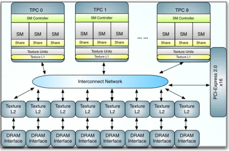
PC I-Exp re ss 2 .0 x1 6 Interconnect Network DRAM Interface DRAM Interface DRAM Interface DRAM Interface DRAM Interface DRAM Interface DRAM Interface DRAM Interface Texture L2 Texture L2 Texture L2 Texture L2 Texture L2 Texture L2 Texture L2 Texture L2 TPC 0 SM Controller SM Share SM Share SM Share Texture Units Texture L1 TPC 1 SM Controller SM Share SM Share SM Share Texture Units Texture L1 TPC 9 SM Controller SM Share SM Share SM Share Texture Units Texture L1 ... ...
Figure 1.1: Block Diagram of GT200 GPU
GPU can be simply considered as a cluster of independent SMs (Streaming Multiproces-sor). Figure 1.1 illustrates the block diagram of GT200. GT200 GPU is composed of 10 TPCs (Thread ProcessingCluster), each of which includes 3 SMs. SMs in one TPC share the same memory pipeline. Each SM further includes scheduler, 8 SPs (Streaming Processor), 1 DPU (Double Precision Unit) and 2 SFUs (Special Function Unit). SP executes single precision floating point, integer arithmetic and logic instructions. The SPs inside one SM, which is the basic computing component, are similar to a lane of SIMD engines and they share the mem-ory resource of the SM like the registers and shared memmem-ory. DPU executes double precision floating point instructions. And SFU handles special mathematical functions, as well as single precision floating point multiplication instructions. If we consider SP as one core, then one GPU processor is comprised of 240 cores.
For Geforce GTX 280 model, with 1296MHz shader clock, the single precision peak performance can reach around 933GFlops. GT280 has 8 64-bit wide GDDR3 memory con-trollers. With 2214MHz memory clock on GTX 280, the memory bandwidth can reach around
GPU Architecture and CUDA Programming Model 25
140GB/s. Besides, within each TPC there is a 24KB L1 texture cache and 256KB L2 Texture cache is shared among TPCs.
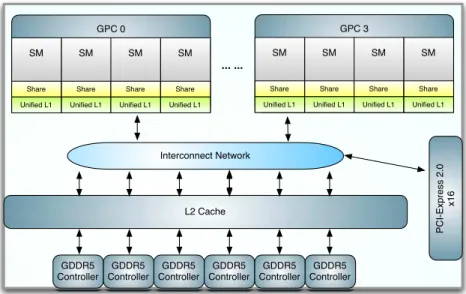
PC I-Exp re ss 2 .0 x1 6 Interconnect Network GDDR5 Controller GDDR5 Controller GDDR5 Controller GDDR5 Controller GDDR5 Controller GDDR5 Controller L2 Cache ... ... GPC 0 SM Share Unified L1 SM Share Unified L1 SM Share Unified L1 SM Share Unified L1 GPC 3 SM Share Unified L1 SM Share Unified L1 SM Share Unified L1 SM Share Unified L1
Figure 1.2: Block Diagram of Fermi GPU
Figure 1.2 is the block diagram of Fermi GPU. Fermi GPU has 4 GPCs (Graphics Pro-cessing Clusters) and in all 16 SMs. The number of SPs per SM increase to 32. The most significant difference is that Fermi GPU provides real L1 and L2 cache hierarchy. Local writes are written back to L1 when register resource is not sufficient. Global stores bypass L1 cache since multiple L1 caches are not coherent for global data. L2 cache is designed to reduce the penalty of some irregular global memory accesses.
As an example, Geforce GTX 580 has a shader clock of 1544 MHz and the theoretical single precision peak performance of 1581 GFlops. The memory controllers are upgraded to GDDR5 and a bandwidth of 192.4 GB/s.
The Kepler GPU’s high level architecture is very close to Fermi GPU. The main difference is the scheduling functional units, which cannot be shown on the block diagram level.
A comparison of the three generations of NVIDIA GPUs is illustrated in Table 1.1. From GT200 to Kepler GPU, the number of SPs increases dramatically, from 240 (GTX280, 65nm) to 1536 (GTX680, 28nm) [75, 74]. Each SM in Fermi GPU consists of 32 SPs instead of 8 SPs on GT200 GPU. On Kepler GPU, each SM (SMX) includes 192 SPs. For GTX280, each SM has 16KB shared memory and 16K 32bit registers. In GTX580, shared memory per SM increases to 48KB and the 32bit register number is 32K. GTX680 has the same amount of shared memory with GTX580 and the register number increases to 64K. However, if we consider the memory resource (registers and shared memory) per SP, the on-die storage per SP actually decreases. The global memory bandwidth actually does not change a lot. Previous generations have two clock domains in the SM, the core clock for the scheduler and the shader clock for the SPs. The shader clock is roughly twice the speed of the core clock. On Kepler (GK104) GPU, shader clock no longer exists, the functional units with SMs run at the same
GT200 Fermi Kepler (GTX280) (GTX580) (GTX680)
Core Clock (MHz) 602 772 1006
Shader Clock (MHz) 1296 1544 1006
Global Memory Bandwidth(GB/s) 141.7 192.4 192.26
Warp Scheduler per SM 1 2 4
Dispatch Unit per SM 1 2 8
Thread Instruction issuing throughput 16 32 128?
per shader cycle per SM
SP per SM 8 32 192
SP Thread Instruction processing throughput 8 32 192?
per shader cycle per SM (FMAD/FFMA)
LD/ST (Load/Store) Unit per SM unknown 16 32
Shared Memory Instruction processing throughput unknown 16 32 per shader cycle per SM (LDS)
Shared Memory per SM 16KB 48KB 48KB
32bit Registers per SM 16K 32K 64K
Theoretical Peak Performance (GFLOPS) 933 1581 3090
Table 1.1: Architecture Evolution
core clock. However, to compare the different generations more easily, we still use the term shader clock on Kepler GPU and the shader clock is the same as the core clock. In the rest of this thesis, all throughput data is calculated with the shader clock.
1.1.3 CUDA Programming Model
The Compute Unified Device Architecture (CUDA) [2, 50] is widely accepted as a program-ming model for NVIDIA GPUs. It is a C-like programprogram-ming interface with a few extensions to the standard C/C++. A typical CUDA program normally creates thousands of threads to hide memory access latency and math instruction pipeline latency since the threads are very light weight. One of the most important characteristics of GPU architecture is that the mem-ory operation latency could be hidden by concurrently executing multiple memmem-ory requests or executing other instructions during the waiting period. The threads are grouped into 1D to 3D blocks or cooperative thread arrasy (CTAs) [57], and further into 1D or 2D grids. The warp is the basic execution and scheduling unit of a SM, and is composed of 32 threads within one block on current NVIDIA GPUs.
All threads have access to global memory space or device memory. Accessing global mem-ory generally takes hundreds of cycles. The memmem-ory accesses by a warp of 32 threads could be combined into fewer memory transactions and referred to as coalesced global memory access. Threads within one block can share data in shared memory and synchronize with a barrier syn-chronization operation. The shared memory has very low latency comparing to global memory.
GPU Architecture and CUDA Programming Model 27
Efficiently utilizing shared memory can significantly reduce the global memory pressure and reduce average memory access latency. The shared memory is organized in banks. Bank con-flict could happen if multiple threads in a warp access the same bank.
Each thread has its own local memory and register resource. Each block is assigned to one SM at execution time and one SM can execute multiple blocks concurrently. The shared memory and register resource consumed by one block has the same lifetime as the block. On the SM, since the memory resource like register file and shared memory is limited, only a limited set of threads can run concurrently (active threads).
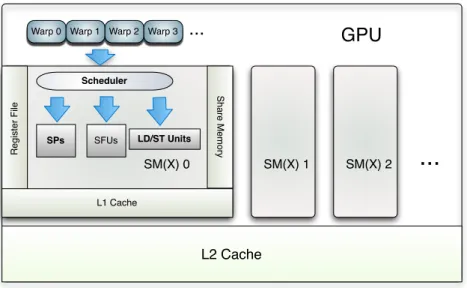
GPU
Scheduler
Warp 0 Warp 1 Warp 2 Warp 3
Sh a re Me mo ry SPs SFUs SM(X) 0
...
LD/ST Units R e g ist e r F ile L1 Cache SM(X) 1 SM(X) 2...
L2 CacheFigure 1.3: CUDA Execution Model on NVIDIA GPUs
Figure 1.3 presents a simplified CUDA execution model. The scheduler uses a score board to select one ready instruction from one of the active warps and then issue the instruction to the corresponding functional unit. There is no penalty to issue instruction other current warp. With this light weight context switching mechanism, some latency can be hidden. However, programmers still need to provide enough number of threads which can be executed concur-rently to get good occupancy [2].
On one hand, the increased SPs per SM require more active threads to hide latency. On the other hand, the register and shared memory limit the number of active threads. For the same application, the active threads that one SP supports actually decreases because of the reduced memory resource per SP from Fermi GPU to Kepler GPU. More instruction level parallelism within one thread needs to be explored.
A CUDA program is composed of host code running on the host CPU, and device code running on the GPU processor. The compiler first split the source code into host code and device code. The device code is first compiled into the intermediate PTX (Parallel Thread eXecution) code [71], and then compiled into native GPU binary code by the assembler ptxas. The device binary and device binary code are combined into the final executable file. The compiling stages are illustrated in Figure 1.4. NVIDIA provides the disassemblerCuobjdump
C Device Code Device Binary PTX Code Fat Binary C Host Code Host Binary Exe File PTXAS
Figure 1.4: Compiling Stages of CUDA Programms
which can convert GPU binary code into human-readable assembly codes [2].
1.2
Performance Prediction of GPU Applications Using
Simula-tion Approach
There are already several simulators for graphics architectures [83, 29, 11, 24]. The Qsilver [83] and ATTILLA [29] simulators are not designed for general purpose computing on GPUs and focus on the graphics features. The Barra simulator [24] is a functional simulator and does not provide timing information. The GPGPU-Sim [34, 11] is a cycle-accurate simulator for CUDA applications executing on NVIDIA GPUs and omits hardware not exposed to CUDA. The following part of this section briefly introduces the approach of GPGPU-Sim simulator.
1.2.1 Baseline Architecture
The GPGPU-Sim simulates a GPU running CUDA applications. Some hardware features of the baseline architecture are collected from NVIDIA pattern files. The simulated GPU consists of a cluster of shader cores, which is similar to SMs in NVIDIA GPUs. The shader cores are connected by an interconnection network with memory controllers.
Inside a shader core, a SIMD in-order pipeline is modeled. The SIMD width depends on the architecture that is to be modeled. The pipeline has six logical stages, including instruction fetch, decode, execute, memory1, memory2 and write back. Thread scheduling inside a shader core does not have overhead. Different warps are selected to execute in a round robin sequence. The warp encountering a long latency operation is taken out of the scheduling pool until the operation is served.
Memory requests to different memory space are also modeled. For off-chip access, or ac-cess to global memory, the request goes through an interconnection network which connects the shader cores and the memory controllers. The nodes of shader cores and memory controllers have a 2D mesh layout.
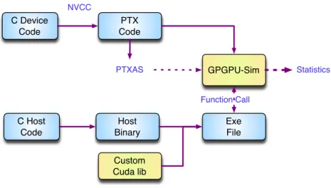
Performance Prediction of GPU Applications Using Simulation Approach 29 1.2.2 Simulation Flow C Device Code PTX Code C Host Code Host Binary Exe File Custom Cuda lib PTXAS GPGPU-Sim Function Call Statistics NVCC
Figure 1.5: Simulation of CUDA Application with GPGPU-Sim
GPGPU-Sim simulates the PTX instruction set. The Figure 1.5 illustrates the simulation flow of GPGPU-Sim. Different from a normal CUDA application compiling and execution, the host binary is linked with custom CUDA library, which invokes the simulation for each device kernel call. The device code is first compiled into PTX code by nvcc. The PTX code serves as the simulation input. The assembler ptxas provides the register usage information to GPGPU-Sim since the register allocation happens when PTX code is compiled into device binary. Then GPGPU-Sim utilizes this information to limit the number of concurrent threads. PTX is a pseudo instruction set and the PTX code does not execute on the actual device. To improve the simulation accuracy and also reduce maintaining effort, a super set of PTX called PTXPlus is designed. PTXPlus has the similar syntax as PTX and can be converted from the assembly code, which can be get from the NVIDIA dis-assembler.
1.2.3 Accuracy
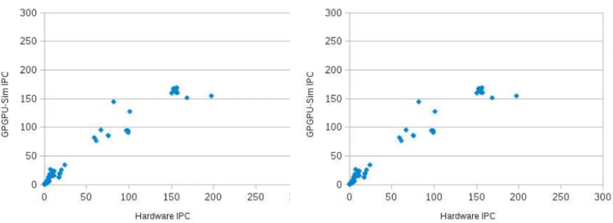
The intention of GPGPU-Sim is not to accurately model any particular commercial GPU but to provide a foundation for architecture researchers. The even though the baseline models can be configured according to one specific GPU model, the modeled architecture is only similar to the actual GPU architecture. In the latest manual of GPGPU-Sim [90], the authors provided a comparison between the simulated execution time with the calibrated GPGPU-Sim, and the actual execution time on the GT200 GPU and Fermi GPU. In terms of IPC (Instructions per Clock), for the Rodinia benchmark suite [19] and using the native hardware instruction set (PTXPlus), GPGPU-Sim obtains IPC correlation of 98.3% and 97.3% respectively. However, the average absolute errors are 35% and 62%.
Figure 1.6: Correlation Versus GT200 & Fermi Architectures (Stolen from GPGPU-Sim Man-ual)
1.2.4 Limitations
The main limitation for simulation approach is that since vendors disclose very few hardware details, it is very difficult to build an accurate simulator for an existing GPU model. And it is very unlikely to build an accurate simulator for the new GPU generation. The baseline ar-chitecture model may differ very much from the real hardware characteristics. The accuracy of the simulator cannot be guaranteed without enough hardware details. It is not safe to draw the same conclusion on a real architecture with the result obtained on the simulation baseline architecture. Thus, it is better to use the simulator to explore different architecture configu-rations. For researchers and developers who study how to improve application performance on existing architectures, the simulator may not be a very good choice. Second, even with an accurate simulator, it is very unlikely for a common developer to use it to understand the per-formance results and make further optimizations because running a simulation would require a lot of time and long learning curve of the tool.
1.3
Performance Projection/Prediction of GPU Applications Using
Analytical Performance Models
For superscalar processors, there is already a rich body of work that proposes analytical models for performance analysis [69, 64, 63, 48, 19, 45, 87, 3, 33]. However, since the general comput-ing on GPU processors is still a fairly new research area, the models and approaches proposed to understand GPU performance results still need a lot of refinement. There exist some inter-esting works about how to project/predict CUDA applications’ performance using analytical or simulation methods. Meng et al. proposed a GPU performance projection framework based
Performance Projection/Prediction of GPU Applications Using Analytical Performance Models31
on code skeletons [61]. Bahsork et al. proposed an analytical performance-prediction moel based on work flow graph (WFG), which is similar to the control flow graph [9]. Hong et al. introduced the MWP-CWP model to predict CUDA application performance using PTX code [40]. Recently, Sim et al. extended the MWP-CWP model and utilize the assembly code of CUDA kernel to predict performance [85]. The quantitative GPU performance model proposed by Zhang et al. is also based on the native assembly code [101]. Kim et al. proposed a tool to analyze CUDA applications’ memory access patterns [49]. Since very little information about the underlying GPU architecture is disclosed, it becomes very unlikely to build accurate simu-lators for each new GPU generation. Beside general performance models for GPUs, there also exist some works of model-driven performance optimization for specific kernels[20, 62, 30].
To optimize a GPU application, some general guidelines are provided. Normally devel-opers needs to vary many parameter combinations to find the optimal solution. However, to thoroughly understand the GPU architecture and the performance result of CUDA applications remains difficult for developers. Tools like NVIDIA Visual Profiler [72] can provide stat data from the GPU hardware counter, such as the number of coalesced global memory access, the number of uncoalesced global memory access and the number of shared memory bank conflict. Normally programmers rely on this kind of tool to optimize their cuda applications. For exam-ple, if many global memory accesses are coalesced, the global memory access pattern might need to be carefully redesigned. However, the information that the profiler provides very few insights into the performance result.
Although simulation approach for certain architectures is available [35], it is not realistic for developers to use simulators to optimize applications since it is very time consuming. What developers need the most is a tool or an approach that does not require a long learning curve and still provides much insight into the performance result. The analytical approach fits this requirement. Generally, analytical GPU performance model does not need all the hardware details but only a set of parameters that could be obtained through benchmarking or public ma-terials. Apparently, analytical approach cannot compete with the simulation approach for ac-curacy. Luckily, the performance prediction results of existing analytical performance models [61, 40, 85, 101, 26] show that we can have still very good approximation of GPU performance. The rest of this section includes several recent analytical performance models for GPU and a brief summary.
1.3.1 MWP-CWP Model
In 2009, Hong et Kim [40] introduced the first analytical model for GPU processors to help to understand the GPU architecture or the MWP-CWP model. The key idea of their model is to estimate the number of parallel memory requests (memory warp parallelism or MWP. Ac-cording to their reported result, the performance prediction result with their GPU performance model has a geometric mean of absolute error of 5.4% comparing to the micro-benchmarks and 13.3% comparing to some actual GPU applications.
The authors claimed that memory instructions’ latency actually dominates the execution time of an application. In the paper, two main concepts are introduced to represent the degree of warp level parallelism. One is memory warp parallelism or MWP, which stands for the maximum number of warps that can access the memory in parallel during the period from the
cycle when one warp issues a memory request till the time when the memory requests from the same warp are serviced. This period is called one memory warp waiting period. The other is computation warp parallelism or CWP, which represents how much computation could be run in parallel by other warps while current warp is waiting for memory request to return the data. When CWP is greater than MWP, it means that the computation latency is hidden by the memory waiting latency and the execution time is dominated by the memory transactions. The execution time can be calculated as 1.1. The Comp p is the execution cycles of one computation period.
Exec cycles = M em cycles ∗M W PN + Comp p ∗ MW P (1.1) Actually, if we compare the two parts of theExec cycles, the Comp p∗ MW P part is a small number comparing to the memory waiting period. The other partM em cycles ∗ M W PN can be simply interpreted as the sum of N warps’ memory accessing latency parallelized by NWP channels. Thus we can simplify the conclusion as when CWP is greater than MPW or there is not enough memory accessing parallelism, the execution time is dominated by the global memory access latency and can be calculated as the memory accessing time of one warp multiplies the number of active warps and then divided by the degrees of memory access parallelism.
When MWP is greater than CWP, it means that the global memory access latency is hidden by the computation latency and the execution time is dominated by the computation periods. The total execution time can be calculated as 1.2.
Exec cycles = M em p + Comp cycles∗ N (1.2)
Similarly, if we compare the two parts of theExec cycles in this case, the M em p part is relatively a small value when each warp has many computation periods. The other part Comp cycles∗ N can be interpreted as the sum of N warps’ computation demand since the computation part of all N active warps cannot be parallelized. So we can draw a simpler con-clusion as when MWP is greater than CPW or there is enough memory accessing parallelism, the execution time is dominated by the computation latency and can be calculated as the com-putation time of one warp times the number of active warps.
1.3.1.1 Limitations
The MWP-CWP model is the first analytical model introduced for GPU performance mod-eling and becomes the footstone of many later GPU performance models. It provides some interesting insight to understand the GPU performance result.
However, the model is too coarse grain since it simply separate an execution of an appli-cation into computation period plus the memory access period. The computation period is the instruction issue latency multiplies the number of instructions. The memory access period is a sum of all the memory access latency. Firstly, the model is too optimistic about the instruction level parallelism to calculate the computation period. Secondly, the model assumes memory transactions from one warp are serialized, which is not true. The performance model essentially
Performance Projection/Prediction of GPU Applications Using Analytical Performance Models33
uses the ratio of computation time to the memory access latency to define whether the execu-tion time is dominated by the memory access latency or the computaexecu-tion latency. The analysis takes an application as a whole entity. However, for many applications, the execution may have difference characteristics in different parts. For example, in some parts, the application may mainly load data from global memory and in other parts, it may mainly do the computation.
The model for uncoalesced global memory access is too rough. In the model, the unco-alesced global memory accesses are modeled as a series of continuous memory transactions. However, the changed pressure on memory bandwidth is not considered. Plus, the shared mem-ory is not specially treated in the model. To effectively utilize shared memmem-ory is essential to achieve good performance on GPU. The model takes the shared memory access instruction as a common computation instruction. The behavior of shared memory access is very complicated. In one shared memory access instruction, if multiple threads within one warp access the same bank, it may introduce bank conflict. The bank conflict normally has a significant impact on ther performance. The new memory hierarchy like unified cache is not considered in the model either.
The model uses the PTX code of an application as the model input. Since the PTX code needs to be compiled into the native machine code to execute on the GPU hardware, it intro-duces some inaccuracy.
1.3.2 Extended MWP-CWP Model
Recently, Sim et al. [85] proposed a performance analysis framework for GPGPU applications based on the MWP-CWP model. This extended model includes several main improvements over the original MWP-CWP model. First, instruction level parallelism is not assumed to be always enough and the memory level parallelism is not considered to be always one. Second, it introduces the cache modeling and the modeling of the shared memory bank conflict. Third, the MWP-CWP model only utilizes information from PTX code. The extended model uses the compiled binary information.
The extended model requires a variety of information including the hardware counters from an actual execution. To get these information, a front end data collector was designed. The collector the CUDA visual profiler, an instruction analyzer based on Ocelot [36], a static assembly analysis tool. After the execution, the visual profiler provides stat information like number of coalesced global memory requests, the DRAM reads/writes, and cache hits/misses. The instruction analyzer mainly collect loop information to decide how many times each each loop is executed. The static analysis tool is used to obtain ILP (instruction level parallelism) and MLP (memory level parallelism) information from binary level. ILP or MLP obtained by the static analysis tool represents the intra-warp instruction or memory level parallelism.
The total execution time Texec is a function of the computation cost Tcomp, the memory
access costTmem and the overlapped costToverlap, and defined as Equation 1.3. Tcomp
repre-sents the time to execute computation instructions (including the memory instruction issuing time).Tmem is the amount of time of memory transactions. Toverlaprepresents the amount of
memory access cost that can be hidden by multithreading.
Tcomp includes a parallelizable part Wparallel and a serializable partWserial. The
serial-izable partWserialrepresents the overhead due to sources like synchronization, SFU resource
contention, control flow divergence and shared memory bank conflicts. The parallelizable part Wparallelaccounts for the number of instructions executed and degree of parallelism.
Tmemis a function of the number of the memory requests, memory request latency and the
degree of memory level parallelism.
Toverlaprepresents the time thatTcompandTmemcan overlap. If all the memory access
la-tency can be hidden,Toverlapequals toTmem. If none of the memory access can be overlapped
with computation,Toverlapis 0.
1.3.2.1 Limitations
The main improvements of the extended MWP-CWP model over the original MWP-CWP model include firstly, runtime information like the number of shared memory bank conflict and DRAM hits/misses is collected using Visual Profiler. Thus the shared memory bank con-flict effect and the cache effect are introduced in the model. Secondly, the assembly code is served as the model input. Thus the instruction level parallelism can be correctly collected.
However, the model requires an actual execution of the program to collect the runtime information, which makes performance prediction less meaningful. The bandwidth effects of uncoalesced global memory accesses and shared memory bank conflict are still not included the model. The bad memory access is only considered to have a longer latency. The modeling of the shared memory access is still too simple since only bank conflict behavior is considered in the serial overheadWserial. Even though the memory level parallelism and instruction level
parallelism are calculated using the assembly code, since the two metrics is for the whole application, the model is still too coarse grain to catch the possibly varied behavior of different program sections.
1.3.3 A Quantitative Performance Analysis Model
In 2011, Zhang et Owens proposed a quantitative GPU performance model for GPU archi-tectures [101]. The model is built on a microbenchmark-based approach. The author claims that with this model, programmers can identify the performance bottlenecks and their causes and also predict the potential benefits if the bottlenecks could be eliminated by optimization techniques.
The general idea of their proposition is to model the GPU processor as three major com-ponents: the instruction pipeline, the shared memory, and the global memory and to model the execution of an GPU application as instructions being served to different components based on the instruction type. With the assumption that non-bottleneck components is covered by the bottleneck component, the application bottleneck is identified by the component with the longest execution time.
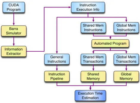
As in Figure 1.7, the Barra simulator [24] is used to get the application runtime information, such as how many times each instruction is executed. Then this information is used to generate the number of dynamic instructions of each type, the number of shared memory transactions and the number of global memory transactions. Since Barra simulator does not provide bank
![Figure 1.4: Compiling Stages of CUDA Programms which can convert GPU binary code into human-readable assembly codes [2].](https://thumb-eu.123doks.com/thumbv2/123doknet/11508055.293991/30.892.183.651.288.518/figure-compiling-stages-programms-convert-binary-readable-assembly.webp)