HAL Id: hal-00955098
https://hal-univ-rennes1.archives-ouvertes.fr/hal-00955098
Submitted on 3 Mar 2014
HAL is a multi-disciplinary open access
archive for the deposit and dissemination of
sci-entific research documents, whether they are
pub-lished or not. The documents may come from
teaching and research institutions in France or
abroad, or from public or private research centers.
L’archive ouverte pluridisciplinaire HAL, est
destinée au dépôt et à la diffusion de documents
scientifiques de niveau recherche, publiés ou non,
émanant des établissements d’enseignement et de
recherche français ou étrangers, des laboratoires
publics ou privés.
Microcrystalline silicon gauges on flexible substrates for
high deformations with high spatial resolution
Yannick Kervran, Sabri Janfaoui, Olivier de Sagazan, Samuel Crand, Nathalie
Coulon, Jean-Philippe Gauthier, Tayeb Mohammed-Brahim
To cite this version:
Yannick Kervran, Sabri Janfaoui, Olivier de Sagazan, Samuel Crand, Nathalie Coulon, et al..
Mi-crocrystalline silicon gauges on flexible substrates for high deformations with high spatial resolution.
Sensing Technology (ICST), 2013 Seventh International Conference on, Dec 2013, Wellington, New
Zealand. pp.603-607, �10.1109/ICSensT.2013.6727724�. �hal-00955098�
Microcrystalline silicon gauges on flexible substrates for
high deformations with high spatial resolution
Y. Kervran, S. Janfaoui, O. De Sagazan, S. Crand, N. Coulon, J. P. Gauthier, T. Mohammed-Brahim
DMM-IETR UMR-CNRS 6164, Université RENNES I, 35042 Rennes Cedex, FRANCE
[email protected]
Abstract
Microcrystalline silicon films are used as piezoresistive material to fabricate resistor and transistor strain gauges. Very small gauges are fabricated allowing the possibility to measure high deformations with both high sensitivity and spatial resolution. Resistor gauges with 5 x 125 µm² smallest size showed a gauge factor of -24 when applying high strains (0.55%, radius of curvature 5 mm). Field effect thin film transistor (TFT) gauges showed a gauge factor of -85 but under slightly lower strains (0.45%, radius of curvature 10 mm). This value is close to strain gauges made of single crystalline silicon (~ 100, regarding the absolute value), but which are not flexible and then cannot support high deformations. The more complex technological process of TFT gauges could reserve their use to the measurement of low deformations when high resolution is required, while resistor gauges could be chosen when focusing on a mix between size and sensitivity in a large range of deformations.
Keywords
: Microcrystalline silicon, strain gauge, spatial resolution, flexible substrate, resistor, transistor1
Introduction
There is now an increasing demand for light and foldable electronics. Numerous worked in robotics [1], health system [2], aeronautics [3] and so on are interested in. To ensure the monitoring of such systems, strain gauges are usually designed to study the electrical response of sensors (e.g. force/pressure sensor with a cavity [4]) to any deformations.
The sensitivity of a strain gauge is defined by the Gauge Factor (GF), the ratio of relative change in electrical resistance (R/R) to relative change in length of a resistor (L/L, the strain ), R/R = GF x (L/L). Two main types of materials are used as strain gauges: metals and semi-conductors. For metals, the most common ones and commercially available, the GF ~ 2 is weak, and the need of long wires to get measurable resistances make their use prohibitive when a high density is needed, like a deformation mapping with high spatial resolution [5]. In the case of semi-conductors, such as single crystalline silicon, the controlled resistivity and its high |GF| ~ 100, due to its high piezoresistivity, can help to reach a high resolution.
The problem is that single crystalline silicon made resistors are rigid even for small sizes, and cannot support high deformations. One solution is to thin enough the silicon wafer on which the resistance is fabricated and to report it on a flexible substrate [6]. However, the costs of thinning and report operations are prohibitive. Another solution is to fabricate silicon resistors directly on a flexible substrate. Deposited silicon films cannot be single crystalline but their structures are amorphous or polycrystalline with some nanometers to micrometers sized grains. Due to this disordered structure, the GF value is lower than 100 but much higher than 2.
Direct process on flexible substrate needs to take care on its chemical and mechanical characteristics. First, it has to support the different chemical solutions and the maximum temperature of the process. Then, other characteristics can be specific: biocompatibility for biological applications, more or less flexibility (depending on the Young modulus), optical transparency in flexible displays field. Polyimide (PI) such as Kapton® can hold 400°C during 120 minutes with 1.2% shrinkage but it is not transparent (and usually used at lower temperatures). Transparent plastic that hold the highest temperature is polyethylene naphthalate (PEN). When annealed, it can reach 180°C with 0.2% shrinkage during 30 minutes. Both are produced by DuPont™ Teijin Films. In this paper, polyimide and PEN are used. To be compatible with the limited maximum temperature reached by PEN, silicon resistors are fabricated on both substrates at a lower temperature than 180°C. This requirement is a challenge to obtain well crystallized silicon. But if the challenge is jumped, gauges made by crystallized silicon deposited on plastics can fulfil all the requirements of high GF and miniaturization using lithography technologies. Previously, authors [7, 8] reported gauges based on crystallized silicon films deposited on flexible substrate at low temperature with a highest GF ~ 20/30 (absolute value). As expected, this factor is lower than single crystalline silicon GF but much higher than metal ones. However, it was given only for weak deformations with a strain lower than 0.25%. For practical use, strain gauges have to measure much higher deformations. That is why, small gauges are here studied in this purpose. 2 types are used: the first one is a basic resistor and the second one is a thin film transistor allowing an expected better sensitivity thanks to the field effect.
2
Resistive Gauges
2.1
Process
Microcrystalline silicon (µc-Si) is used as piezoresistive material. The µc-Si films are deposited at 165°C in a Plasma Enhanced Chemical Vapor Deposition (PECVD) reactor using silane, hydrogen and argon. Previously [9], we have shown that the crystalline fraction in µc-Si films is improved when adding argon in the usual silane and hydrogen gas mixture [10]. Here, 1.5 sccm silane, 75 sccm hydrogen and 75 sccm argon (1% dilution of silane in Ar-H2
mixture) are used. Then, arsine as N-type doping gas is added in the gas mixture to vary the resistivity/conductivity of µc-Si film in a very large range depending on the arsine flow. Thus, the highest conductivity obtained is 12 S.cm-1 for a 50 nm thick N-type µc-Si film, and 3x10⁻⁹ S.cm-1 for the same thickness but undoped film. So, the electrical resistance of the gauge can be adapted depending on the needs.
To study the answer of microcrystalline silicon film based strain gauges, differently sized resistors are fabricated on polyimide sheets covered by 50 nm thick silicon nitride deposited by RF-PECVD at 150°C using silane and ammonia. The slightly N-type doped µc-Si film is deposited and islands patterned by Reactive Ion Etching (RIE) with SF6 plasma. Aluminium film is
then deposited by Joule Effect Evaporation and patterned by wet etching to form different gaps L between electrodes. The total structure uses the known Transmission Line Method (TLM, Figure 1).
2.2
TLM
Figure 1: The TLM structure designed. The width of the resistors is W. The gap L between the electrodes varies between 5 µm to 160 µm. It doubles each time between 2 successive contacts. The pads (1mm²) are designed in order to be able to place the probes during bending tests.
The aim is to separate the effects of the gauge resistances from the contact resistances. Indeed, the total resistance of a gauge with its 2 contacts is given by R = L/(eW) + 2RC where and e are respectively
the resistivity and the thickness of the µc-Si film, L the distance between electrodes (the length of the gauge), W their width and RC is the contact resistance of one
metal/semi-conductor interface. The resistance of the aluminium routing is neglected (RAl << RµcSi). Then
plotting the measured R as a function of L leads to a straight line (if contacts are ohmic) with a slope proportional to the resistivity . The piezoresistivity of the present µc-Si material can be then checked during tensile tests by bending the gauges with different radii of curvature using homemade tools (Figure 3).
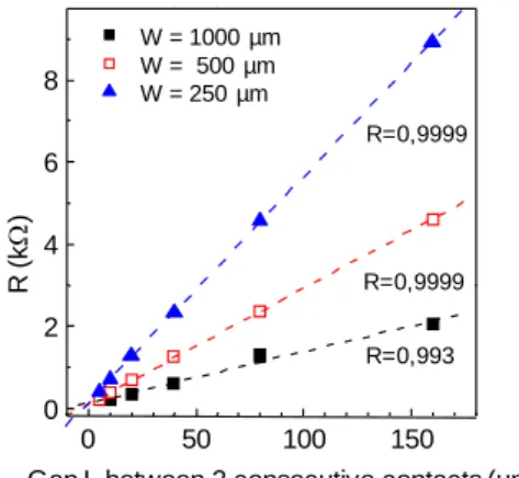
16 TLM structures with 4 W (1000, 500, 250 and 125 µm) are fabricated on the same 5 x 5 cm² polyimide sheets. Each structure has 6 L (5, 10, 20, 40, 80, 160 µm), for a total of 24 different resistances. In each cell, resistors with same W and different L are measured. This allows checking the linearity of the variation of the resistance when L varies. Figure 2 shows this linearity for 3 cells with different W.
Figure 2: Variation of the resistances with 3 W (250, 500 and 1000 µm) when the distance L between the electrodes varies from 5 to 160 µm. The linearity of the curves is shown through the values of the correlation factor R of the linear fit.
The correlation factor of the fit is given in the figure to show the excellent linearity of the curves. This shows that contacts between aluminium electrodes and µc-Si film are ohmic. The slightly lower factor obtained for W = 1000 µm is due to the smallest resistances about the same order than the contact resistance. The resistivity of the µc-Si film can be determined then from the slopes of these straight lines. Its calculated value is 0.137 cm.
2.3
Bending Tests
After checking the true value of the resistivity of µc-Si film independently on contacts resistance, the TLM structures have been bent using homemade tools with 5 different radii of curvature (2.5, 2, 1.5, 1 and 0.5 cm, tensile tests). For each radius R, the strain applied to the structure is calculated using a simplified model. The real structure of the resistor is a stack of 3 films: 50 µm polyimide substrate, 50 nm thick top silicon nitride and 100 nm thick microcrystalline silicon films. But the model is constituted only by the
µc-Si
Al
W 0 50 100 150 0 2 4 6 8 W = 1000 µm W = 500 µm W = 250 µm R (k )Gap L between 2 consecutive contacts (µm) R=0,9999
R=0,9999
R=0,993
substrate and the silicon nitride film due to its much higher Young modulus (270 GPa) than the other films. Thus, the mechanical behaviour of the resistors is mainly defined by the behaviour of the silicon nitride. Equation (1) [11] links the radius of curvature R to the strain applied to the resistor for the simplified model.
2 21
1
2
1
2
R
d
d
S f(1)
In this equation, dS and df are the thicknesses of the
substrate and the silicon nitride films respectively.
and are defined by
S f S f d d Y Y ; where YS
and Yf are the Young modulus of the substrate
(2.5 GPa) and the silicon nitride film (270 GPa) respectively.
Figure 3: Optical images of homemade tools used to bend the structure with different radii of curvature for tensile tests. The structure is bent in the same direction of the current flow, to study only the longitudinal GF.
The procedure to study the sensitivity of the gauges consists in a first measurement of the 24 resistors without bending (flat substrate). Then, the TLM structure is stuck on the holder with the highest radius of curvature and the resistors measured. After that, the TLM structure is removed and the resistors measured again without bending (flat substrate). The previous steps are renewed by decreasing the radius of curvature. However, it is important to note that a first bending at the smallest radius must be applied to get a good linearity in the following results.
The most important result for practical applications is the comeback of the resistors to their initial value (when the resistors are flat) after each bending. Figure 4 shows an example of 6 resistances with the same W as a function of the gap L between the electrodes measured after each bending corresponding to decreased radii of curvature from 2.5 cm to 0.5 cm. For each L, the resistances show a relative difference with their original flatten value inferior to 1% and no differences between the linear straights can be highlighted which shows the good comeback.
Figure 4: Variation of the resistance for W = 1000 µm when the distance L between the electrodes varies from 5 to 160 µm. The variation is measured when the substrate is flat and after each successive bending.
Figure 5 presents the mean relative variation of the 24 measured resistances as a function of the strain calculated with the equation (1). The means are represented because no influence of the size of the resistances on the sensitivity has been noted and for each point, the standard deviation of the 24 data is also represented. Measures are more dispersed for high strains due to the difficulty to place the probes during high bending. The gauge factor, defined by the slope of the fit, is GF ~ -24 (with a minus sign because the resistances decrease during tensile tests). The value is similar to the gauge factor of crystallized silicon films given in references [7, 8]. But the value is given here for higher strains, with a maximum of 0.55%, corresponding to a curvature radius of 5 mm. Moreover, the small size of the gauges studied in this work (minimum of 5 x 125 µm²) allows the possibility to integrate such strain gauges when high spatial resolution is required.
Figure 5: Relative variation of the gauge resistances as a function of the tensile strain. Each point is the mean of 24 resistances and the standard deviation is represented. The slope of the fit is GF ~ -24.
GF = -24 -14 -12 -10 -8 -6 -4 -2 0 0,0 0,2 0,4 0,6 Δ R /R ( % ) Strain ε (%) 0 50 100 150 0 2 R (k )
Gap L between 2 consecutive contacts (µm)
R=0,9999 W=1000µm 0 0.1 0.2 0.3 0.4 0.5 0.6 0.5cm 1cm 1mm Strain ε (%)
3
Thin Film Transistor Gauges
3.1
Process
Microcrystalline silicon (µc-Si) based N-type Top-Gate TFTs are fabricated on 5 x 5 cm² sheets of PEN at a maximum temperature of 180°C. The sheet of PEN is encapsulated on both sides with 250 nm thick silicon nitride. A 100 nm thick layer undoped µc-Si is deposited in the same conditions as for resistive gauges. After that, a 70 nm thick layer arsenic doped µc-Si is deposited in the same manner as the undoped µc-Si using a mixture of silane, hydrogen and arsine. A first photolithography step is used to define drain, source and channel regions. The µc-Si doped layer is etched by SF6 plasma in a RIE
reactor to define source and drain regions. Then, a second photolithography step is necessary in the purpose to insulate transistors one from each other. The undoped µc-Si is etched by SF6 plasma. This step is followed by
an RCA cleaning. After that, 300 nm thick silicon nitride film acting as gate insulator is deposited by PECVD at 150°C using mixture of silane, nitrogen and ammonia. A third photolithography step is used to open windows for drain and source contacts. The silicon nitride film is etched by SF6 plasma. A layer of
aluminium is deposited by thermal evaporation, and a fourth photolithography step is used to define the drain, source and gate electrodes. Aluminium is etched by wet way. The final structure is presented in Figure 6.
Figure 6: Structure of µc-Si Top-Gate TFT.
3.2
TFTs sensitivity to mechanical strain
The previous TFTs are electrically characterized when submitting to different curvature radii starting from infinite radius (flat TFTs) to a radius of 1.5 cm. An example of the drain-source current IDS versus thegate-source voltage VGS characteristic, plotted in linear
regime under a drain-source voltage of VDS = +1V, is
given in Figure 7.
The on-state current at constant VGS increases under
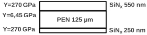
tensile stress. To calculate the GF of these transistors, we have to plot this current as a function of the strain which is calculated from the radius of curvature by using, as previously for resistors, a model of the real structure of the TFT (stack of 5 films): 250 nm thick bottom silicon nitride film, 125 µm PEN substrate, 250 nm thick top silicon nitride, 100 nm thick µc-Si film, 300 nm thick silicon nitride gate insulator, 300 nm thick aluminium gate contact.
Figure 7: IDS vs VGS characteristic plotted in linear regime
under VDS = +1V. TFT channel width is W = 100 µm and
length is L = 20 µm.
Considering the much higher Young modulus of silicon nitride (270 GPa) and the different thicknesses, the total bended structure is considered constituted by 3 layers only: bottom 250 nm thick silicon nitride, 125 µm PEN substrate and a top 550 nm thick silicon nitride (Figure 8).
Figure 8: Mechanical model of the total TFT structure.
Taking this modelled structure with the substrate embedded between 2 films, the equation (2) [11] can be used to calculate the strain applied to the TFTs on the top of the structure. In this equation, dS, df1 and df2
are the thicknesses of substrate, top and bottom silicon nitride films respectively. and are defined by
S f S f S f
d
d
d
d
Y
Y
2 2 1 1;
;
where YS and Yfare the Young modulus of the substrate (6.45 GPa) and the silicon nitride film (270 GPa) respectively.
Figure 9 shows the relative variation of the on-state current (IDS/IDS), taken at VGS = 30V and VDS = 1V, as
a function of the calculated strain. This variation is presented here for 4 differently sized TFTs, varying the width for the same length or varying the length for the same width. Whatever the size is, the plots can be fitted by a straight line with the same slope. For the present TFTs, the GF is -85. The minus sign is due to the definition of the gauge factor which implies ∆R/R, while here I/I is calculated. This value is very important in comparison with the resistive gauges made of the same microcrystalline silicon film.
1
1
1
2
2
1
1
2 1 2 2 1 2 2 1 1 2 2 2 1 2 1 0
d
Sd
fd
fR
R
(2) -20 -10 0 10 20 30 10-12 10-11 10-10 10-9 10-8 10-7 10-6 IDS (A) VGS(V) W/L = 100 µm /20µm VDS= + 1V PEN 125 µm SiNX250 nm SiNX550 nm Y=270 GPa Y=270 GPa Y=6,45 GPa
Its value is in the same order than single crystalline silicon resistive gauges.
Figure 9: Relative variation of the on-current of differently sized TFTs as a function of the tensile strain. The slope of the fit is GF ~ -85.
4
Conclusion
Two types of strain gauges were studied in this work. Both used the piezoresistivity of microcrystalline silicon films, deposited directly crystallized on plastic substrates at low temperature by using silane, hydrogen and argon gas mixture. The use of silicon films led us to use usual photolithography technologies.
The first type is a µc-Si film resistor with 2 electrodes. The smallest size was 5 x 125 µm², demonstrating a high spatial resolution. The reliability of the technological process was shown and a gauge factor of -24 was demonstrated even when applying high strain of 0.55% (for a radius of curvature of 5 mm).
The second type is a field effect TFT. The size of these TFTs is similar to the resistors (larger by a factor ~2) but the gauge factor of -85 is much higher, close to the value of single crystalline silicon gauges. The maximum strain applied was 0.45% (for a radius of curvature of 10 mm). Then, even if the technological process is more complicated but reliable, TFT gauges could be used to measure low deformations requiring high resolution.
5
References
[1] T. Someya, Y. Kato, T. Sekitani, S. Iba, Y. Noguchi, Y. Murase, H. Kawaguchi, T. Sakurai, “Conformable, flexible, large-area networks of pressure and thermal sensors with organic transistor active matrixes” Proc. Nat. Acad. Sci. 102, pp. 12321-12325 (2005)
[2] S. Jung, T. Ji, V. K. Varadan, “Point of care temperature and respiration monitoring sensors
for smart fabric applications” Smart Mater. Struct. 15, pp. 1872-1876 (2006)
[3] A. Casano, P. Capoluongo, S. Campopiano, A. Cutolo, M. Giordano, F. Felli, A. Paolozzi, M. Caponero, “Experimental modal analysis of an aircraft model wing by embedded filter Bragg grating sensors” IEEE Sensors J. 6, pp. 67-77 (2006)
[4] H-J. Kwon, W-C. Choi, “Design and fabrication of a flexible three-axial tactile sensor array based on polyimide micromachining”, Microsystem Technologies, Vol. 16, Issue 12, pp. 2029-2035 (2010)
[5] G. Y. Yang, V. J. Bailey, G. Lin, W. C. Tang, J. H. Keyak, “Design of Microfabricated Strain Gauge Array to Monitor Bone Deformation In Vitro and In Vivo”, Proc., IEEE 4th Symp.
Bioinformatics Bioeng., pp. 30-37 (2004) [6] S. M. Won, H-S. Kim, N. Lu, D-G. Kim, C. Del
Solar, T. Duenas, A. Ameen, and J. A. Rogers, “Piezoresistive Strain Sensors and Multiplexed Arrays Using Assemblies of Single-Crystalline Silicon Nanoribbons on Plastic Substrates”, IEEE Transactions On Electron Devices, Vol. 58, No. 11 (2011)
[7] P. Alpuim, S.A. Filonovich, C.M. Costa, P.F. Rocha, M.I. Vasilevskiy, S. Lanceros-Mendez, C. Fria, A. Torres Marques, S. Roares, C. Costa, “Fabrication of a strain sensor for bone implant failure detection based on piezoresistive doped nanocrystalline silicon” J. Non-Cryst. Sol. 354, pp. 2585–2589 (2008)
[8] P. Alpuim, V. Correia, E. S. Martins, J. G. Rocha, I.G. Trindade, S. Lanceros-Mendez, “Piezoresistive silicon thin film sensor array for biomedical applications” Thin Solid Films 519, pp. 4574-4577 (2011)
[9] K. Kandoussi, C. Simon, N. Coulon, K. Belarbi, T. Mohammed-Brahim, “Nanocrystalline silicon TFT process using silane diluted in argon-hydrogen mixtures”, J. Non Cryst. Sol. 354, pp. 2513-2518 (2008)
[10] A. Matsuda, “Microcrystalline silicon: Growth and device application”, J. Non-Cryst. Sol. 338-340, pp. 1-12 (2004)
[11] H. Gleskova, S. Wagner, Z. Suo, “Failure resistance of amorphous silicon transistors under extreme in-plane strain” Appl. Phys. Lett. 75, pp. 3011-3013 (1999) 0 0.2 0.4 0 0.1 0.2 0.3 0.4 0.5 W/L = 100 µm /20 µm W/L = 80 µm /20 µm W/L = 100 µm /40 µm W/L = 80 µm /40 µm IDS / IDS Strain(x10-2%) R=85%GF = -85 (%)