HAL Id: hal-01897147
https://hal.archives-ouvertes.fr/hal-01897147
Submitted on 24 Mar 2020
HAL is a multi-disciplinary open access
archive for the deposit and dissemination of
sci-entific research documents, whether they are
pub-lished or not. The documents may come from
teaching and research institutions in France or
L’archive ouverte pluridisciplinaire HAL, est
destinée au dépôt et à la diffusion de documents
scientifiques de niveau recherche, publiés ou non,
émanant des établissements d’enseignement et de
recherche français ou étrangers, des laboratoires
The FAZIA setup: A review on the electronics and the
mechanical mounting
S. Valdré, G. Casini, N. Le Neindre, M. Bini, A. Boiano, B. Borderie, P.
Edelbruck, G. Poggi, F. Salomon, G. Tortone, et al.
To cite this version:
S. Valdré, G. Casini, N. Le Neindre, M. Bini, A. Boiano, et al..
The FAZIA setup: A
re-view on the electronics and the mechanical mounting. Nucl.Instrum.Meth.A, 2019, 930, pp.27-36.
�10.1016/j.nima.2019.03.082�. �hal-01897147�
The FAZIA setup: a review on the electronics
and the mechanical mounting
IS. Valdr´ea,∗, G. Casinia, N. Le Neindreb, M. Binic,a,1, A. Boianod, B. Borderiee, P. Edelbrucke,1,
G. Poggic,a, F. Salomone, G. Tortoned, R. Albaf, S. Barlinic,a, E. Bonnetg, R. Bougaultb, B. Bougardb,
G. Bruline, M. Brunoh,i,1, A. Buccolac,a, A. Camaianic,a, A. Chbihij, C. Ciampic,a, M. Cicerchiak,l,
M. Cinauserol, D. Dell’Aquilam, P. Desruesb, J. A. Due˜nasn, D. Fabriso, M. Falorsic,a,1, J. D. Franklandj,
C. Frosinc,a, E. Galichete,p, R. Giordanoq, F. Gramegnal, L. Grassie, D. Gruyerb, M. Guerzonii,
M. Henrib, M. Kajetanowiczr, K. Korcyls, A. Kordyaszt, T. Koziku, P. Lecomtej, I. Lombardov, O. Lopezb,
C. Maiolinof, G. Mantovanik,l, T. Marchil, A. Margottii, Y. Merrerb, L. Morellij, A. Olmia,1, A. Ordined,
P. Ottanellic,a, C. Painb, M. Pa lkau, M. Pˆarlogb,w, G. Pasqualic,a, G. Pastorec,a, S. Piantellia, H. de
Pr´eaumontb, R. Revenkoj, A. Richarde,1, M.F. Rivete,2, J. Ropertj, E. Rosatoq,d,2, F. Saillantj,
D. Santonocitof, E. Scarlinic,a, S. Serrai, C. Soulete, G. Spadacciniq,d,1, A. A. Stefaninic,a, G. Tobiaa,
S. Upadhyayau, A. Vanzanellad, G. Verdev, E. Vientb, M. Vigilanteq,d, E. Wanline, G. Wittwerj,
A. Zucchinii
aINFN — Sezione di Firenze, 50019 Sesto Fiorentino, Italy
bLPC Caen, Normandie Univ, ENSICAEN, UNICAEN, CNRS/IN2P3, LPC Caen, 14000 Caen, France cDipartimento di Fisica, Universit`a di Firenze, 50019 Sesto Fiorentino, Italy
dINFN — Sezione di Napoli, 80126 Napoli, Italy
eInstitut de Physique Nucl´eaire, CNRS-IN2P3, Univ. Paris-Sud, Universit´e Paris-Saclay, 91406 Orsay, France fINFN — Laboratori Nazionali del Sud, 95123 Catania, Italy
gSUBATECH, EMN-IN2P3/CNRS-Universit´e de Nantes, Nantes, France hDipartimento di Fisica, Universit`a di Bologna, 40127 Bologna, Italy
iINFN — Sezione di Bologna, 40127 Bologna, Italy jGANIL, CEA/DRF-CNRS/IN2P3, 14076 Caen, France kDipartimento di Fisica, Universit`a di Padova, 35131 Padova, Italy
lINFN — Laboratori Nazionali di Legnaro, 35020 Legnaro, Italy
mNational Superconducting Cyclotron Laboratory, Michigan State University, East Lansing, Michigan 48824, USA nDepto. de Ingenier´ıa El´ectrica y Centro de Estudios Avanzados en F´ısica, Matem´aticas y Computaci´on. Universidad de
Huelva, 21071 Huelva, Spain
oINFN — Sezione di Padova, 35131 Padova, Italy
pConservatoire National des Arts et M´etiers, 75141 Paris cedex 03, France qDipartimento di Fisica, Universit`a di Napoli, 80126 Napoli, Italy
rNowoczesna Elektronika, 30-109 Cracow, Poland
sInstitute of Nuclear Physics, Polish Academy of Sciences, 31-342 Cracow, Poland tHeavy Ion Laboratory, University of Warsaw, 02-093 Warszawa, Poland
uFaculty of Physics, Astronomy and Applied Computer Science, Jagiellonian University, 30-348 Cracow, Poland vINFN — Sezione di Catania, 95123 Catania, Italy
w“Horia Hulubei” National Institute for R&D in Physics and Nuclear Engineering (IFIN-HH), P.O.BOX MG-6, Bucharest
Magurele, Romania
Abstract
In this paper the technological aspects of the FAZIA array will be explored. After a productive commissioning phase, FAZIA blocks started to measure and give very useful data to explore the physics of Fermi energy heavy-ion reactions. This was possible thanks to many technical measures and innovations developed in
I 2018. This manuscript version is made available under the CC-BY-NC-ND 4.0 license.c
http://creativecommons.org/licenses/by-nc-nd/4.0/
∗Corresponding author
Email address: [email protected] (S. Valdr´e)
1Retired
2Deceased
the commissioning phase and tuned during the first experimental campaigns. This paper gives a detailed description of the present status of the FAZIA setup from the electronic and mechanical point of view, trying also to trace a path for new improvements and refinements of the apparatus.
Keywords: FAZIA, front-end electronics, data acquisition, telescope array, heavy-ion reactions, nuclear
physics
PACS:29.85.Ca, 29.40.Wk
1. Introduction and specific requirements
FAZIA (Forward-angle A and Z Identification Array) is a modern and innovative three-layer telescope [Si + Si + CsI(Tl)] array. This review paper follows the work of R. Bougault et al. [1] where the R&D phase of the FAZIA project was carefully described. In this paper we will give a detailed overview on the technological aspects of the final detector array; in particular, we will focus on the electronics, the data flow and the mechanical aspects of the apparatus.
The multi-detector FAZIA aims at detecting and identifying particles and fragments produced in heavy-ion reactheavy-ions around Fermi energy. The main requirement of FAZIA is the modularity and portability: in fact, FAZIA was designed to measure in various laboratories, in different setups and coupled to several detectors. Another important objective is to maximise unit identification for charges and masses of detected nuclei. In the present situation, we clearly discriminate charges up to Z ∼ 55 and masses up to Z ∼ 25. This goal was achieved using custom detectors produced following a well-studied recipe [2, 3] and using original electronics with novel pulse-shape discrimination (PSD) techniques [4–6] based on high speed analog-to-digital converters with rates up to 250 MS/s and 14-bit resolution. The whole electronics is embedded in the proximity of the telescopes inside the vacuum chamber.
The commissioning runs of FAZIA proved the capability to integrate inside the scattering chamber all the electronics required for silicon detectors and scintillators read-out by photodiodes. This very innovative electronics includes pre-amplifiers, analogue chains, high speed converters, read-out logic, high voltage de-vices and pulse generator for analogue chains. Indeed, the first experimental campaigns proved that it is possible to integrate, on the same multi-layer card, some potentially noisy power-supplies (such as switch-ing regulators) with sensitive low-noise pre-amplifiers whose power-supply rejection ratio is not high. This integration has been possible by applying strict electromagnetic compatibility design guidelines.
The great complexity and the fine granularity of the apparatus implies a difficult scalability and thus a relatively poor angular coverage: in fact a 16-telescope block, which is the smallest independent FAZIA unit, covers only around 0.05 % of the full solid angle at 1 m distance from the target. Indeed, the next FAZIA schedule foresees the mounting of a 12-block array in 2019, coupled with INDRA detector array [7] at GANIL to increase the angular coverage.
The electronic cards are described in Sec. 2. Both the “block” electronics, that is mounted directly next to detectors inside the scattering chamber (in vacuum) and the devices outside the chamber are detailed. Afterwards, a functional description of the apparatus follows (Sec. 3): in particular the clock distribution (Sec. 3.1), the data packet structure (Sec. 3.2), the trigger logic (Sec. 3.3), the data flow (Sec. 3.4), the possibility of coupling (Sec. 3.5), the acquisition (Sec. 3.6), and the slow control (Sec. 3.7) are presented. In Sec. 4 the adopted mechanical solutions necessary to hold and to cool the block electronics and to align the detectors are described. Finally, in Sec. 5, we give an overview on all the innovative aspects of the FAZIA modular array and the next improvements we are going to realise.
2. Description of the electronic boards
The first feature which could be noticed when looking at the FAZIA apparatus is the absolute scarcity of electronic racks outside the scattering chamber (Fig. 1). In fact, the so-called regional board (RB) is the only electronic card placed outside (see Sec. 2.4) and it performs the functions of a standard “event
building” card. Only two connections per block are necessary: a 48 V (6 A) power supply line and a 3 Gbit/s full-duplex optical link used to transfer data, to synchronise the clocks, to send triggers, and to manage any block parameter via slow control.
48 V DC power supply
Regional
board
Back plane Half-bridge and power supply cards Block card FEE card #0 FEE card #7 Back plane Half-bridge and power supply cards Block card FEE card #0 FEE card #7vacuum
air
to
acquisition
Block ‘n’ Block ‘0’Figure 1: Schematic representation of the FAZIA electronic cards inside and outside the scattering chamber. For a detailed description see the text.
Inside the vacuum chamber, the basic element of the FAZIA array is the block, which consists of 16 detector telescopes. The telescopes are connected to 8 front-end electronic (FEE) cards (see Sec. 2.2), which feature, among other components, charge sensitive pre-amplifiers, ADCs, Si bias voltage regulators, and FPGAs for data handling. Up to two telescopes can be connected to each front-end card. All the FEE cards are connected to a “Block Card” (see Sec. 2.3) via a common backplane, which hosts also two power supply boards (see Sec. 2.1). The Block Card (BC) is mainly devoted to handle I/O operations and to merge data coming from the FEE cards. Power Supply (PS) and Half Bridge (HB) cards produce and monitor the voltages needed to the other boards on the block. The FAZIA blocks communicate with the event building electronics via the Block Card through the 3 Gbit/s optical link. A metallic housing covers all the block; there is also a metal screen around the BC, PS and HB cards to avoid that electromagnetic emissions from DC/DC converters reach the FEE cards. All the electronic cards of the block are supported by (and firmly screwed to) a copper plate in which water can flow for cooling. The FEE cards and the electromagnetic shield structure have been designed at IPN Orsay; BC, PS and HB boards have been developed at INFN – Naples; the copper plates are built at INFN – Bologna and Firenze; the RB has been designed at Jagiellonian University in Krak´ow (Poland) in collaboration with INFN – Naples.
2.1. Power supply
The DC levels needed by the block electronics (BC and FEEs) are produced by two cards that are both connected to the backplane: Half Bridge and Power Supply. As previously mentioned, the FAZIA block needs only an external 48 V DC line to work. This voltage is provided to the Half Bridge card, which performs a high power conversion to 22 V DC (14 A max) and 5.5 V DC (70 A max) by means of two commercial switching converters (CUI VHB350 series). These devices have an insulation, with low parasitic capacity, between primary and secondary stage to avoid ground loops. To reduce the electromagnetic interferences produced by the converters, a particular two stage filter was added at the 48 V input line: the first stage is a BALUN (balanced-to-unbalanced) transformer used to balance the interferences and the second stage contains a common-mode transformer to filter them. The output 5.5 V voltage is split into two lines: one (4 A max) is dedicated to the Block Card and it is equipped with an over-current protection circuit; the
other (40 A max) is used to power the FEE cards and it is controlled by a power MOSFET. The 22 V output line, together with the 5.5 V voltage monitor line, is connected to the Power Supply card via the backplane. The PS card main task is to produce and monitor the voltages required by the Block Card and the FEE cards. In particular, it uses DC/DC switching converters to transform the 22 V input to 13 V DC (2 A), −9 V DC (1 A), 6 V DC (5 A), and −6 V DC (2 A). The 13 V and −9 V lines, which are used to bias the pre-amplifiers, have an additional linear regulator to reduce the high frequency ripple. The PS card produces also a negative HV line, currently used to bias the CsI(Tl) crystal photodiodes, which is user settable in the range 0–600 V DC (4 mA max). Due to the huge range of the output voltage, it was not possible to use only a flyback converter. In particular, a step down power supply stage (controlled by the same driver) is placed before the standard flyback circuit implemented with the UC3842 driver. In this way, we obtained that the voltage at the input of the flyback stage is reduced when the output voltage decreases. Moreover, to achieve a better commutation precision of the driver Pulse-Width Modulation (PWM) stage, a circuit that modulates the switching frequency in function of the set voltage was implemented.
The PS card is also equipped with a PIC microcontroller which continuously measures the voltages and the current flowing through the power supply lines; it also monitors the temperature of the board and, in the case of overheating, it shuts down the FEE card lines.
2.2. FEE cards
The core of the FAZIA block is the front-end electronic card [8]. Up to 8 FEEs can be mounted on each block. The area of these boards (299 × 88 mm2) is subdivided into three parts (Fig. 2). The first stage
embeds all the low-noise analogue electronics (pre-amplifiers, amplifiers and anti-aliasing filters). At the opposite side, the FEE hosts the switching power-supplies which are sources of electromagnetic disturbances and thus are placed, by design, far from the analogue stages. In the middle part, among many other components, two Xilinx Virtex-5 (model XC5VLX50) FPGA chips (one for each telescope and called “A” and “B” from now on), a PIC microcontroller, and 12 ADCs are mounted. The printed circuit board has 16 layers on which 1700 components are located on the top surface only. The power consumption of a card is about 30 W. The connection toward the heat sink is done by two aluminium plates: one pressed and sticked on the upper side of both FPGAs and one entirely covering the back side of the card. This second sheet has a shelf that is screwed on the main cooled copper plate of the block (see Sec. 4.3).
Figure 2: Picture of a front-end electronic card without the protection and dissipation plates. The three stages in which the card is subdivided are highlighted.
Analogue stage. Six charge pre-amplifiers (three per telescope) are placed on each front-end card just next
to the detector connectors. Their architecture is based on a folded cascode amplifier and the output dynamic range is 8 V for a total energy of 4 GeV (∼ 300 MeV Si-equivalent for the CsI(Tl) channels), providing a sensitivity of 2 mV/MeV for both Si1 and Si2. The detector signals are AC coupled with a 10 nF capacitor
to block the bias voltage. A circuitry (containing a DAC) is added to the pre-amplifier output stage to tune the output offset voltage. This function allows one to set the analogue chain baseline close to the bottom level of the ADC input range, in order to better exploit the available dynamic range of the ADC. The baseline level could be remotely controlled in any moment via a slow control command, since the DAC input buses are directly connected to the FPGAs. The analogue lines then split to have multiple channels per detector. In particular, for the first Si stage, we have three paths: high range charge signal (QH1), low range charge signal (QL1) and current signal (I1). For the second Si stage we have the high range charge signal (Q2) and the current signal (I2). For the CsI stage we have only one charge signal (Q3). The high range (low gain) signals (QH1, Q2 and Q3) are attenuated by a factor 4, to adapt the 8 V dynamic range of the pre-amplifiers to the 2 V input range of the ADCs. On the contrary, the low range (high gain) signal (QL1) is amplified by a factor 3. The current signals (I1 and I2) are obtained by analogue differentiation of the Si1 and Si2 pre-amplifier outputs. All the six signals described above pass through an anti-aliasing filter before being sampled by the ADCs.
A square pulse generator has been built on the front-end card in order to test the analogue chain response. It is also useful to verify possible amplification changes during data taking (which, incidentally, have never been observed up to now). The generator is based on a simple MOSFET clocked switch connected to the inputs of all the pre-amplifiers through a capacitor. The user can change the amplitude, the frequency, and the duty cycle of the pulse generator via slow control instructions. The pulser amplitude is set by a DAC, whose input bus is connected to the front-end PIC microcontroller. Frequency and duty cycle depend on the switch clock, that is generated by the FPGA “B”. Alternatively, an external clock could be used by setting the appropriate slow control register.
Digital stage. In the previous paragraph, the twelve signals (six per telescope) that are generated in the
analogue stage of the card were described. QH1, Q2 and Q3 signals are connected to 14-bit, 100 MS/s analog-to-digital converters with a 2 V input range. Since we have a 2 mV/MeV sensitivity from the pre-amplifier and then we reduce the signal by a factor 4, at the end we get an energy conversion factor of about 4.1 ADC units per MeV for QH1 and Q2 signals. The relatively slow sampling rate is more than sufficient for energy measurements. Moreover, the very high effective number of bits (ENOB = 11.4) of the ADCs guarantees an accurate reconstruction of the released energy inside the detector. QL1, I1 and I2 signals are sampled by 14-bit, 250 MS/s ADCs with a 1.5 V input range. Considering the QL1 signal, we have again a 2 mV/MeV sensitivity from the pre-amplifier but in this case we amplify the signal by a factor 3, so at the end we get an energy conversion factor of about 66 ADC units per MeV (16 times larger with respect to the corresponding high range signal). The low range line is thus very useful to identify and measure energy of particles that produce small energy losses within the first Si layer, such as light fragments up to Z ∼ 10. Another important feature of the QL1 signal is the possibility to use it for timing, because it is acquired by a fast sampling ADC. Current signals are also acquired by 250 MS/s 14-bit ADCs. In fact, because of their fast time evolution, their shape cannot be faithfully reconstructed by interpolation if sampled at 100 MS/s. Indeed, the current signal represents an accurate image of the charge collection process within the detector and allows the best identification performances via pulse-shape discrimination for ions stopping in the first stage of the telescope [9–11].
The twelve analog-to-digital converters are read by the two FPGAs: the six signals from the first telescope are handled by FPGA “A” and the six signals from the second telescope are handled by FPGA “B”. The two programmable arrays compute in real time the energy through digital filtering. They also generate local triggers, data packing and transmission to the acquisition (see Sec. 3.4).
Also the 8-bit PIC microcontroller lies in the digital part of the FEE card. It is capable to accept and execute commands received through a serial slow control link and it can subsequently write and read the slow control FPGA registers by Serial Peripheral Interface (SPI) link. As previously said, the PIC controls the pulser amplitude. It controls also the high voltage devices (described in the next paragraph) and reads, by means of a dedicated 16-bit ADC, the current flowing through the Si detectors. When this reverse current increases, the PIC automatically increases the HV device output to compensate the voltage drop on the 10 MΩ bias resistor and to maintain the biasing voltage of the silicon detectors at constant value. This function is quite important to preserve good PSD during an experiment. Finally, the PIC also gets
temperature values coming from embedded sensors located in several critical positions on the cards.
Converters stage. The voltage conversion stage is placed just close to the backplane connector. The low
voltage power supply part includes four switching converters and more than 20 linear regulators. Four high voltage devices are also embedded on the board. The high voltages are generated from a common 5.5 V input and their purpose is to bias the silicon detectors of the two telescopes. The architecture of the HV modules is based on a switching regulator and a transformer. The high voltage devices for Si1 can ramp up to 300 V with a precision of less than 0.1 V. The HV device for Si2 can ramp up to 500 V with the same absolute precision. The HV functions and values are remotely controlled via the PIC microcontroller. The integrated high voltage device represents a new and original solution within the nuclear physics community, as it is embedded into one single electronic card operating under vacuum.
2.3. Block card
The main task of the Block Card (shown in Fig. 3) is to retrieve all the data coming from the FEE cards and to build from them a partial event. The main communication path between the BC and FEE cards is implemented with 24 serial buses in a “star” configuration: each front-end card is reached by three 400 Mbit/s buses. Two buses connect each FEE card to the BC and one goes from the BC to each FEE. The implementation of these fast serial links was done using Xilinx “ISERDES” and “OSERDES” cores. To align and synchronize data, a programmable delay was also added before the ISERDES unit. Moreover, other common signals reach every FEE card from the Block Card: i.e. the validation signal, the external pulser clock and the slow control line. Every kind of communication between BC and FEEs passes through the backplane. On the contrary, the communication with the event building electronics takes place through a 3 Gbit/s optical link. In particular, the Block Card hosts a small form-factor pluggable (SFP) optical transceiver that supports two (RX and TX) SX fibers (850 nm wavelength) with a LC connector.
Figure 3: Picture of a Block Card. In the center, the FPGA is covered by the heat sink. In the right side, the SFP transceiver
used to communicate with the Regional Board can be seen.
Communications and data sorting are handled by a Xilinx Virtex-5 FPGA (model XC5VFX70T), to-gether with the fundamental task of capturing a special packet from the optical link to produce a synchro-nized clock (see Sec. 3.1). The Block Card contains also a photodiode which reads another optical fiber and a 50 MS/s ADC to sample the signal coming from it. To exploit the full ADC range, a variable gain amplification circuit was also implemented. This system is used as an extra synchronization method, as it will be described in Sec. 3.1. Finally, the BC features a microSD slot. If a memory card with a special file is present in the slot when the board is switched on, the block identification number (ID) is read from that file. In this way it’s very easy to change the block ID during the experiment. The block ID is the only way to distinguish the blocks when a slow control command is sent. The microSD card could also be used to reload the FPGA firmware with a “.xsvf” file.
2.4. Event building electronics
The regional board (Fig. 4) is a 6U size VME card (operating outside the reaction chamber, in air) whose main tasks are: to read data from the FAZIA blocks and form a complete event, to analyze the triggers from the blocks and possibly send validations to them, to handle slow control requests from many PCs and eventually to communicate with acquisition servers. The RB is an evolution of the “test card” developed by INFN – Naples group. That card featured an USB protocol to transmit data to the acquisition system and it was capable to handle up to 8 blocks. The test card was widely used to develop many features implemented in the regional board, such as the internet protocol on the on-board FPGA.
The RB can manage up to 36 blocks and, in case of configurations that need a higher number of blocks, multiple regional boards may be interconnected using optical links and/or the VME bus. However, this feature has not been yet implemented.
Figure 4: Picture of the regional board with highlights of the most important features: (a) VME connectors and CPLD, (b) FPGA and crystal oscillators, (c) special connectors for block communication; (d) SFP slots; (e) LEMO connectors and CENTRUM port.
In addition to the VME bus, regional board connections include six special connectors for block commu-nications, three SFP slots for RB interconnection and communication with acquisition (through Ethernet protocol), four LEMO connectors (“veto in”, “veto out”, “trigger in” and “trigger out”) in LVTTL logic for trigger coupling with other devices and a port for event synchronization among many compatible detectors. The connectors for block communications allow the installation of an optical translator over each of them. At the other end of the optical translator, a compact 12-fiber connector is placed. Each translator handles up to twelve mono-directional fiber connections (RX or TX), thus two translators are needed to operate up to twelve blocks (four translators for up to 24 blocks and all the six translators for up to 36). The port for event synchronization uses the CENTRUM technology developed at the GANIL laboratory (Caen, France). This technology was chosen in view of the forecast coupling of FAZIA with the INDRA detector array, which is installed at GANIL and already uses CENTRUM protocol. All the features and communications (except the VME bus management) are handled by a Xilinx Virtex-5 FPGA (model XC5VTX150T). The VME bus is operated by a Xilinx CPLD (model XC95144XL) that is directly connected to the FPGA. The 5 V operating voltage is supplied by the VME bus.
3. Functional description of the electronics
3.1. Clock distribution
FAZIA is designed to measure over a broad range of beam energies. On some application, mainly with low energy beams, the time of flight (ToF) technique is very useful and the clock synchronization among all the ADCs is necessary. In fact, if the ADCs in different blocks had independent clocks, the accuracy of the time measurement could not be better than one clock cycle (4 ns or 10 ns depending on the kind of ADC). So, to synchronize all the sampling ADCs, they must be provided with exactly the same clock on all the cards. The clock distribution tree is schematically represented in Fig. 5 and it is detailed here. The primary clock is generated on the regional board: there are two crystal oscillators set at 125 MHz and 150 MHz and both are connected to the FPGA chip. The former is used only to clock the Ethernet part of the FPGA project. The latter is used to generate (inside the FPGA) a 25 MHz clock, and to clock the built-in GTX transceivers, which are used to send and receive data from the blocks through the optical link. The transceivers are devices embedded inside the FPGA. In our case they convert 16-bit data at 150 MHz (2.4 Gbit/s) to a serial line at 3 Gbit/s and vice versa. The missing 1.25 factor in the data rate comes from the 8b/10b coding (see Sec. 3.2) of the serial line. Xilinx GTP and GTX transceivers are very suitable to implement a connection with fixed latency, as they can provide an extremely reduced clock skew [12].
Block RX GTX Block RX GTX 125 MHz oscillator 150 MHz oscillator Digital Clock Manager Block TX GTX Packet builder Ethernet GTX Block RX GTX ... ... Acquisition and slow control to blocks from blocks 150 MHz 25 MHz FPGA Regional Board 25 MHz VCXO 150 MHz VCXO PLL PLL RX / TX GTX Packet catcher to and from regional board Block Card FPGA
FAN IN FAN OUT
100 MHz VCXO PLL 250 MHz VCXO PLL ADC ADC ADC ADC ADC ADC FPGA ... to FEEs FEE
Figure 5: Schematic representation of the FAZIA clock distribution, which was designed in order to sample all the signals with the same phase. Further details in the text.
The optical fibers leaving the regional board enter the scattering chamber and reach the various blocks. They are connected to the SFP optical translators on the block cards. The signals eventually arrive inside the block card FPGAs, where they are de-serialized by GTX transceivers. As briefly introduced in the previous section, the BC has a peculiar system to recover the 25 MHz clock from the optical link: on the card there is a voltage controlled crystal oscillator (VCXO), connected to a phase-locked loop (PLL) device, which is used to clock the FPGA. The PLL reference is the signal recovered from the fiber by the FPGA itself. So, when the BC is switched on, the PLL is not locked and the FPGA is clocked by a 25 MHz signal that is uncorrelated with the 25 MHz signal generated on the regional board. Then the block card starts to catch the special K28.5 sequences (see Sec. 3.2) from the optical link and generates the synchronized 25 MHz signal that enters into the PLL device. At this point the PLL is locked and so is the FPGA clock. The PLL output is also split into eight outputs that reach the FEE cards through the backplane. The front-end cards use the phase-locked 25 MHz signal to produce (using VCXO and PLL devices) 100 MHz and 250 MHz frequencies. Finally, these signals are used to clock the ADCs and the FPGAs. Due to the physiological delays between clock edges and ADC sampling, practically the various sampled signals are
not exactly synchronous, since the delays are not identical among the ADCs. The methods to reduce the residual asynchronism, of the order of 100 ps, are currently under study and they will be the subject of another work.
The phase-locked 25 MHz clock on the FEEs is used also to increment a universal 15-bit timestamp counter. To ensure that all the cards are assigning the same timestamp at the same moment, a “time tag zero” signal (TTSync) is sent on the optical fibers by the RB every time that the timestamp counter goes overflow (1.31 ms).
To improve the block cross-synchronization, an external sinusoidal signal (the same for all blocks) could be sampled by the block cards at 50 MS/s. Time marks extracted from sinusoidal waveforms are very precise, even when the sampling rate is not very high [13]. This method allows to check the clock synchronization among blocks with a precision down to 10 ps. The 50 MHz clock is generated by means of VCXO and PLL from the synchronized 25 MHz clock, as also the 150 MHz reference used to clock the GTX devices on the Block Card.
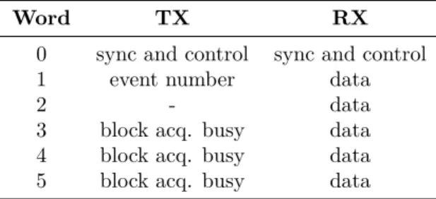
3.2. Packet structure
Since each block is connected with the regional board using only an optical link, the packet structure should be optimized to reduce the data overhead while transmitting all the needed information. The optical link is composed of two fibers: one is used to transmit data to the block (TX) and the other to receive (RX). In both directions data are structured in packets of six 16-bit words and the 8b/10b encoding is used. That means that each byte, when is sent on the fiber, is converted into a 10-bit frame: this conversion helps to provide enough state changes to allow clock recovery. Converting 8-bit sequences to 10 bits means also that some 10-bit sequences have no corresponding 8-bit data. One of these sequences (called “K28.5”) is used to distribute and synchronize the master clock among all the blocks (see Sec. 3.1).
Word TX RX
0 sync and control sync and control
1 event number data
2 - data
3 block acq. busy data 4 block acq. busy data 5 block acq. busy data
Table 1: Summary of the packet structure used in the data transmission between the RB and the blocks. More details in the text.
The first 16-bit word of the packet is always a special synchronization and control frame, both in TX and RX transmission. In particular, the first 8 bits are not defined and they are substituted by the K28.5 sequence in the 8b/10b conversion. The whole packet structure is summarized in Tab. 1 and detailed in the next two paragraphs.
3.2.1. TX packet structure
As said before, the first frame of the transmitted packet is used by the block card to synchronize the master clock via the K28.5 sequence. The remaining 8 bits have the following use:
bit 7 validation signal generated by the RB (see Sec. 3.3); bit 6 slow control TX line (see Sec. 3.7);
bit 5 TTSync signal (see Sec. 3.1); bit 4 global reset of all blocks; bit 3:0 not assigned.
When a validation signal is sent, the second frame of the TX packet contains the 12-bit event number used to check the consistency in the event building phases (see Sec. 3.4). The third frame is not used. The last three frames are used to selectively block the data transmission from the blocks. In fact, when a regional board FIFO dedicated to a specific block is about to be completely full, the RB must block the data acquiring process only from that block. That is achieved by writing on a TX frame a block ID followed by its acquisition status (enabled/disabled). The involved block always reads the last three TX frames searching for its ID: if it is found, the block reads the acquisition enable bit and updates its own status.
3.2.2. RX packet structure
The first frame of the received packet is, also in this case, a synchronization and control word and the first part is again the K28.5 sequence. The remaining 8 bits of the first RX frame are the following:
bit 7 GTT flag (see Sec. 3.4);
bit 6 slow control RX line (see Sec. 3.7); bit 5:1 block trigger multiplicity (see Sec. 3.3); bit 0 not assigned.
The other five frames of the packet contain the data flow coming from the block.
3.3. Trigger logic
On both FPGAs of the front-end cards, fast trapezoidal shaping filters are implemented on the QH1, Q2 and Q3 signals in order to generate local triggers. There are also slow control registers to adjust, for each channel, the filter parameters (rising edge and flat top lengths), the low threshold and the high one. Usually, the filter is set at a 200 ns rising edge and a 200 ns flat top: these values do not affect the sustainable event rate, which is limited by the data acquisition (see Sec. 3.4). For each front-end, the user can also choose the trigger timeout, the trigger source (logic OR among any combination of Si1, Si2 and CsI) and the kind of threshold: i.e. one may use the low threshold only (trigger is produced when the maximum amplitude of shaped signal is larger than it) or both low and high thresholds (trigger is produced when the maximum amplitude of shaped signal is between them). The local triggers generated by the FEEs reach the block card through 16 dedicated lines (one per telescope) on the backplane.
FAZIA trigger system is multiplicity based: on each block, the BC counts the local triggers and sends the total to the regional board every 40 ns through the optical link. The RB collects all the multiplicity values coming from each block and applies up to eight programmable rules. For each one the user can choose (via slow control) the blocks checked by the rule, the multiplicity threshold and the downscale factor
K. The regional board will then integrate inside a time window the multiplicities coming only from the
blocks specified by the rule, and it will produce a “rule trigger” only if the integrated value overcomes the multiplicity thresholds. The trigger is then accepted once every K occurrences. The logic OR among all the rule triggers is eventually the global trigger signal. The RB then checks if there are any alerts: FPGA data buffers are almost full, the GTT flag (see Sec. 3.4) from any block is true or there is an external veto from the “veto in” LEMO connector; if there is at least one alert, then a veto flag is issued. In these cases, except when there is only an external veto, the flag is also sent to the “veto out” LEMO connector. The “trigger out” LEMO connector is true when there is a global trigger without the veto flag. The main output of the trigger component on the regional board is the validation signal: it is produced when the veto flag is false and the global trigger or the external trigger from the “trigger in” LEMO connector are true. The user may also choose to work in “slave” mode (when coupling FAZIA with other devices): in this case the validation is only produced when the veto flag is false and the external trigger is true. In any case the validation signal is sent at a 25 MHz rate to every block via the optical links, captured by the block cards and distributed to every FEE through the backplanes. Together with the validation signal, also an event number, generated by a counter on the regional board FPGA, is always sent to the FEEs using the same path.
3.4. Data flow
On both FPGAs of the front-end cards, four trapezoidal shaping filters are implemented, in addition to the trigger shapers described in the previous section, to calculate in real time the energy released in each stage of the telescope. There is one shaper on the QH1 signal, one on Q2 and two on Q3. In fact, the CsI(Tl) signal has a “fast” and a “slow” filter in order to exploit the well known fast − slow technique [14] to identify the light ions that stop in the last stage of the telescope. As in the case of the trigger shapers, all the rising edge and flat top lengths of the filters are user adjustable. Usually, the filters on QH1 and Q2 were set at a rise time of 2 µs and a flat top of 1 µs. Rise time and flat top for Q3 shapers were set respectively at 2 µs and 10 µs for the slow filter and at 2 µs and 500 ns for the fast one. These values do not affect the sustainable rate because it is limited by the maximum acquisition rate (∼2000 ev/s). Since a faster rate is not affordable, the beam intensity can be accordingly chosen to avoid pile-up and dead time. In addition to being shaped, all the signals (including also QL1, I1 and I2 that have no shaper) are continuously stored in circular buffers with dimension N ≤ 1024, settable via slow control.
When a front-end card FPGA receives a validation, all the raw signals are transferred from their circular buffers to FIFO memories, whose lengths are adjustable via slow control up to a maximum of 4096 samples (∼ 41 µs) for QH1, Q2 and Q3 signals and 8192 samples (∼ 33 µs) for QL1, I1 and I2. At the same time, the acquisition thresholds are checked. These thresholds are again user programmable via slow control and act on the energy shaped signals. If any of the QH1, Q2, Q3 “fast” and Q3 “slow” shaped signals exceeds its respective acquisition threshold, then all the telescope signals are marked for acquisition. A single large FIFO memory is finally used to store the whole local event from the telescope handled by the FPGA. On this memory, if the telescope is marked for acquisition, the six waveforms are transferred together with the four maximum values of the shaped signals and the event number sent by the RB. Between each front-end card and the block card, the data travel on two 400 MHz serial buses (introduced in Sec. 2.3), thus capable to offer a throughput of 800 Mbit/s. The buses are connected to the FPGA “A” on the FEE side, so data sampled by the telescope “B” must pass through FPGA “A”. If any of the FIFO memories on the front-end card is about to fill up, the Global Trigger Throttle (GTT) flag is raised and the RB is vetoed.
When a block card FPGA receives the validation signal, it enters a state where it starts to read the FIFO memories on the front-end cards. The event number written inside the data coming from each FEE is checked and the event is discarded if the number is less than expected. If the actual number is greater than expected, instead, the FEE is skipped but the data are kept for the next event. In this way the block card builds a coherent partial event and stores it in a FIFO buffer waiting to transfer it to the regional board. Inside the partial event, also the external sinusoidal signal (see Sec. 3.1) is stored.
After the generation of the validation signal, the regional board enters a state where it starts to read the FIFO memories on the block cards. In complete analogy to the block card behavior, the RB checks the event number written inside the data coming from each block and the event is discarded if the number is less than expected. If the actual number is greater than expected, instead, the block is skipped but the data are kept for the next event. In this way the regional board builds a full coherent event and stores it in a large FIFO buffer. The RB adds also some trigger information (i.e. number of accepted and vetoed triggers in the last ten seconds) to allow the calculation of the dead time. The FIFO memory is continuously read by a component of the FPGA code that produces Ethernet frames using the User Datagram Protocol (UDP) and send them to the acquisition system through a optical fiber connected to a SFP translator. The user may specify up to 16 machines (sending their IP and MAC addresses via slow control) to which data will be sent. The RB will send an event to the first computer, then another to second and so on. Then it will start again from the first. In this way the dead time due to computing time is minimized. The maximum throughput obtained with the Ethernet communication is about 800 Mbit/s.
3.5. Coupling with other detectors
The regional board features some programmable auxiliary connections which can be used to couple FAZIA with other detectors. In particular, they will be used soon to measure together with INDRA at GANIL. The coupling is done on different levels. The lowest is the trigger level: to ensure a common dead time between FAZIA and INDRA we need to properly interconnect the trigger in/out and veto in/out
LEMO connections (see Sec. 3.3) between the two detectors. The second level consists in the generation of a timestamp: this is performed thanks to the CENTRUM module, which is an absolute timestamp generator connected to both apparatuses. When FAZIA generates a validation signal, it also sends a timestamp request to the CENTRUM system, which dispatches to the RB a frame containing a 48-bit timestamp and a 32-bit event number, plus a 16-bit checksum. A similar packet is sent to INDRA when it produces a request. The FAZIA regional board, after checking the checksum, inserts the CENTRUM frame inside the data flow that is sent to the acquisition. The third and highest level is done by NARVAL, an acquisition system developed by IPN Orsay (France). NARVAL receives data from both INDRA and FAZIA acquisitions and merges those events with timestamp differences smaller than a pre-defined (and reaction-dependent) coincidence window, producing global events composed of data from both the apparatuses.
Of course this system is designed to be as general as possible and it may be used in the future also to couple FAZIA with other detectors than INDRA. Moreover, both CENTRUM and NARVAL technologies support the connections of many apparatuses, so one may also think to easily couple three or four different devices with FAZIA.
3.6. Acquisition
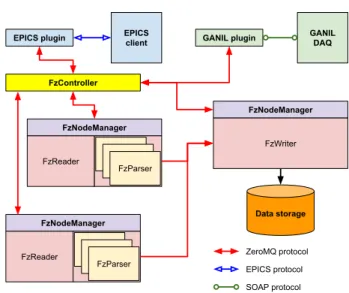
The FAZIA acquisition (DAQ) has been developed and it is currently maintained by INFN – Naples. FAZIA DAQ is a multi-threaded and multi-machine system, written in C++ language and consisting of different classes (DAQ modules) that exchange messages and events through ZeroMQ sockets [15]. The main DAQ modules are the following:
FzReader It acquires raw data coming from the Regional Board by listening to the dedicated UDP socket.
Then it forwards the data to FzParser thread pool.
FzParser Each FzParser includes a Finite State Machine (FSM) able to analyze and validate each acquired
event in order to put all the information inside a structured format based on the Google Protocol Buffers [16]. Multiple FzParser threads can run on a multi-core machine in order to benefit from parallel execution of tasks. Each thread eventually forwards data to the FzWriter module through a 10 Gbit/s dedicated network.
FzWriter This module stores data in files and directories with Google Protobuf data format. It also runs
a data spy in order to allow on-line data processing and analysis by external data visualization tools.
FzNodeManager It is a local supervisor for FzReader/FzParser or FzWriter that run on each FAZIA DAQ
deployed machine. It sends a report on module status to FzController and it receives run control and setup commands for module management.
FzController It is a global supervisor for all FzNodeManager modules. It offers a global view on whole
cluster status and it accepts commands for FAZIA DAQ setup and run control.
Fig. 6 shows the overall architecture of FAZIA DAQ. Some plugins have also been developed to interact with different Run Control systems. These plugins profit of the ZeroMQ network layer of FzController in order to control the data acquisition from different clients (e.g. EPICS or SOAP). This feature of FAZIA DAQ makes it very suitable and flexible for integration and coupling with other experiments and detectors. For example, a GANIL plugin was developed to couple FAZIA with INDRA: it is a C++ class of the DAQ which allows the remote control of FAZIA acquisition from NARVAL system using the SOAP protocol. At the same time, the plugin sends data to NARVAL using a TCP/IP connection.
3.7. Slow control
As illustrated in the previous sections, slow control instructions permit to control almost every aspect of the electronics. The commands, in the form of UDP packets, can be sent by any PC in the same subnet where the regional board is located. The RB analyzes the frame to check if the instruction is for the regional board itself. If it is, then the board executes the command and immediately sends a reply. If not, the RB
EPICS plugin GANIL plugin
FzController
FzNodeManager
FzReader FzParserFzParser FzParser
FzNodeManager
FzWriter
FzNodeManager
FzReader FzParserFzParser FzParser Data storage EPICS client GANIL DAQ ZeroMQ protocol EPICS protocol SOAP protocol
Figure 6: Schematic representation of the FAZIA DAQ system
forwards to all the blocks the message via the optical links. On every block, the instruction is dispatched via the backplane to every card containing a PIC (FEEs, PS, and BC). Since the slow control frame uniquely identifies the card to which it is intended, only that card answers and the reply is returned to regional board. In every case, the RB transmits back the reply message to the PC that has sent the request.
When the slow control request is not for the RB, it must be converted into a standard 115.2 kbit/s serial signal which can be correctly read by the PIC devices on the PS, BC or the FEEs. In particular, in the regional board FPGA code, a universal asynchronous receiver-transmitter (UART) device is implemented. The UART converts the slow control frames received via the Ethernet device into a slow serial data flow which is sent on the optical fibers to all the blocks. Of course, since the slow control bit is sent on the fiber at a 25 MHz rate (see Sec. 3.2.1), the 115.2 kbit/s serial data flow is oversampled. Vice versa, when the RB receives a slow control reply from a block as a serial data flow, this flow is deserialized by the same UART component described above.
4. Mechanical solutions
4.1. Detector holding mechanics
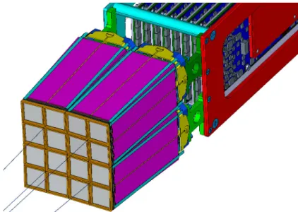
A rendering of the FAZIA detectors is shown in Fig. 7, where silicon pads and CsI(Tl) crystals can be spotted. The 16 telescopes, which form a block, are arranged in a 2 × 2 matrix of quartettos. A “quartetto” is a self-consistent sub-structure of four telescopes in a 2 × 2 configuration. In the figure, the pad precise alignment is also shown. Indeed, each quartetto axis (perpendicular to the surface of the four Si pads) points to the target. This configuration has been achieved through a fixed geometry and thus without degrees of freedom. Our choice has been to build the various supports for a distance of 100 cm between the target and the first Si layer. This value has been chosen as a compromise between detector granularity and solid angle coverage. Moreover, 100 cm is the minimum distance from the target which guarantees a negligible channeling contribution (see below) and a sufficient flight base for time of flight identification.
The detector supporting mechanics has been designed focusing on two main goals. The first is the reduction of all the dead regions between quartettos and on external edges. As a matter of fact, considering a single block, the active area is 84 % of the total front side. The second important goal is the precision of the telescope orientation, in order to reduce the channeling effects. In fact, our silicon detectors are cut in such a way that the particles which perpendicularly impinge on the sensors do not travel along crystal axes [3, 6]. By means of a laser mirroring method (see Sec. 4.4) applied to the reflective Si pad surfaces, we obtained that the orientation misalignment is typically less than 1.5◦; larger values have been rarely
Figure 7: Rendering of the detectors and their support mechanics. Orientation axes of quartettos are also shown.
observed in pads with misplacements or bad gluing. Those two objectives imposed the choice of a proper material to build silicon pad holders. We chose the 7075 aluminium alloy, also used in avionics, because it is precisely machinable and light but, at the same time, it is robust even in thin layers. The supports for the 2 × 2 Si pad matrices (Fig. 8) were built using wire electrical discharge machining. This technique, which softly acts on the bulk, reduces the strains so that the final piece maintains its planarity and details, needed for a good and precise gluing of the silicon pads and the matching between different parts. We remind that a telescope is composed of two silicon detectors followed by a CsI(Tl) crystal so, to form a quartetto, two similar 2 × 2 silicon frames should be locked one on top of the other by means of very thin grooves and ridges. The four CsI(Tl) scintillators are fixed to a central cross-shaped support, which is again made of 7075 aluminium alloy. The strength of this alloy is particularly important for this piece, since it must hold the four crystals (weighing 0.72 kg) and all the silicon pads as a cantilever.
Figure 8: A silicon pad holder with mounted detectors is shown: the grooves and the ridges needed to lock two holders in
position could be seen. The kapton strips, used to connect the sensors to the front-end electronics, are soldered to the metal and µ-bonded to Si pads.
The fastening between the detectors and the rest of the block is relatively simple, in order to allow an easy replacement of the detector “nose”. In this way, when some detectors are damaged, one can replace the whole nose in a reasonable time. Usually, the insertion of the kapton strips into the FEE female connectors is the longest operation.
The above described design and its practical implementation are particularly delicate and many tech-nicians and engineers, from Bologna, Florence and Naples INFN departments, contributed with their work and expertise.
4.2. Frame for the INDRA-FAZIA campaign
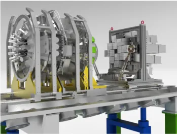
Figure 9: INDRA-FAZIA mechanical drawing. It consists of the usual 4π INDRA multi detector setup, where the first five
rings have been removed to ensure the backward angular coverage from 14◦to 176◦and twelve FAZIA blocks, from 1.5◦to
14◦, divided in four triplets. The whole set-up is hold in the already existing INDRA vacuum chamber at GANIL.
The INDRA-FAZIA experimental phase at GANIL is foreseen during the period 2019–2023. It consists of several nuclear physics experiments with different beams (e.g. Ca, Ni, Kr, Sn and Xe) at various energies (from 25 to 80 MeV/u) on a large variety of targets. It will use the coupling between the multi detectors INDRA and FAZIA. This set up will be fitted in the already existing INDRA vacuum chamber at GANIL. The forward part of the 4π INDRA multi detector is going to be replaced by the new FAZIA array in order to benefit from its better isotopic, energy and angular resolution. The first five INDRA rings (from 1.5◦
to 14◦) will be replaced by twelve FAZIA blocks (Fig. 9) as described previously. Those twelve blocks will
be divided in four triplets. A triplet consists of three FAZIA blocks in a “L” configuration. The blocks are mounted inside a metallic structure and fixed by brackets. This triplet frame holds many handles, various towing rings and also two removable arms in order to help the mounting and the handling inside the vacuum chamber. The main chassis, holding the four triplets, is constituted by a vertical square Elcom based structure, where the four angles have been reinforced with thick stainless steel plates. The triplets are then fixed to each four angles of the vertical main square frame via screws on the thick plates. An intermediate angled brace between the triplets and each angle of the main square frame fixes the geometry of the blocks, i.e. the distance from the target and the polar angles respect to the beam axis where the detectors pointed out. For the first experiment at GANIL this intermediate brace has been designed to ensure a one meter distance to the target and a minimum (maximum) polar angles of 1.5◦ (14◦). The vertical main square
frame is eventually screwed to a movable platform which uses the already existing INDRA vacuum chamber rails, enabling the right positioning distance to the target. Two remotely controlled thick disk shields, with different diameters (a small one protecting the angles from 0.85◦to 3.1◦and a big one from 0.85◦to 5◦), have
been designed to protect the silicon detectors during beam focalization or data taking to avoid radiation damage [17] with stopped heavy ions.
The whole final setup with twelve FAZIA blocks weights around 230 kg (a complete single FAZIA block weights slightly less than 15 kg) and it is foreseen to be towed by a crane if necessary. The CAD design and building of the whole support frame for the twelve blocks have been designed at the Laboratoire de Physique Corpusculaire de Caen, LPC Caen (France).
4.3. Cooling
Since a single FAZIA block absorbs almost 300 W, a very efficient cooling solution must be adopted to operate under vacuum. The final setup consists in a thick copper plate, on which all the cards are screwed on. The conduction is ensured by thermal grease between each card and the copper surface. The copper plate has been designed in order to efficiently distribute the liquid flow along the entire surface which holds the 8 FEE cards. Solving the conflict between the internal pipes for the liquid flow and the many screw holes needed to ensure mechanical and thermal coupling of the electronic boards has been a difficult issue. In total, we have about 100 screws. The adopted solution has been to start from a copper slab 8 mm thick having two main internal in-out pipes running longitudinally on the two sides of the plate. The liquid distribution is then ensured in the copper volume through eight transversal holes, drilled in the plate and joining the input-output main lateral pipes. These transversal holes have variable diameters along the plate length in order to compensate for the pressure drop at the various distances from the entrance/exit tube fittings.
Outside the scattering chamber a powerful chiller (ACW LP60) is mounted to refrigerate the water (with 30 % alcohol or glycol) flowing through all the blocks. The temperature of the cooling liquid is kept at about 10◦C. To ensure an independent cooling for each block a so called “clarinet” device has been built
to dispatch the fluid to all the cooling circuits. It was designed at the Grand Acc´el´erateur National d’Ions
Lourds(GANIL).
4.4. Laser angle measurement
To conclude this review on the FAZIA technological solutions, a notable mention goes to a method that the collaboration implemented to precisely measure the polar angles ϑ and ϕ of the detectors with respect to the beam direction. First of all, a piece of beam line beyond the scattering chamber is dismounted to allow the mounting of a laser. This laser, aligned with the centre of beam line and the target, is fired in the opposite direction with respect to the beam. In place of the target a mirror is then mounted in such a way that its centre is exactly on the path of the laser. The mirror equipment is mounted in a gimbal configuration allowing the rotation around two orthogonal axes: the inclination and declination can be controlled via two precise stepping motors. The fine regulation of the “zero” position (when the laser bounces back in the same direction from where it impinged on the mirror) is set once via micrometric screws. Then, by regulating the two mirror angles (using the stepping motors) up to when the reflected laser beam impinges on the centre of a telescope, it is easy to obtain its ϑ and ϕ angles via a reading of the encoded current position of the motors. The centre of the telescope is determined by visual inspection with an estimated accuracy of the order of 1 mm, corresponding to ∼30 accuracy on angle measurement. The described technique is in fact a
simplified version of a method used by the collaboration for the FIASCO experiment (see Sec 2.1 of [18]).
5. Conclusions and future improvements
In this review paper we examined the most peculiar and innovative features of the FAZIA telescope array from the technological point of view. To summarise, some of the most important characteristics of FAZIA are the compactness and modularity: since FAZIA is structured in independent blocks, various geometry configurations are possible; moreover, all the analogue chains operate under vacuum, very close to the detectors, so that electronic noise pick-up and signal distortion along the transmission lines are greatly reduced. Another factor that should not be neglected is the optimisation of the analogue stages done in the last years: in fact, the pre-amplifiers were designed after many tests performed in the past with prototype telescopes [19]; a similar consideration is valid also for the choice of the ADCs. The combination of pre-amplifiers which have a very high dynamic range and low noise with converters that have a well balanced
design in term of ENOB and sampling rate permits to obtain a good energy resolution in a very wide spectrum of particle energies and charges (from Am α sources to heavy nuclei with energies of the order of 4 GeV). The clock distribution is another fundamental part of the FAZIA apparatus. Thanks to a very complex design that uses fixed latency optical connections and many PLL devices on each electronic card, it is possible to achieve a synchronisation among all the acquired channels within 100 ps.
Finally, other important aspects of FAZIA are its flexibility and upgradability. In fact, all the electronic boards contain programmable devices which are steadily maintained and updated to include new features. Indeed, one can implement new firmware solutions on the on-board FPGA after that a given algorithm has been tested off-line using the entire sampled waveforms previously acquired. For example, in this respect we are going to implement the pulse-shape discrimination of silicon signals directly on-board, by adding the search of the current signal maximum on the front-end card FPGA code. Another feature which may be added to the same code is an energy shaper on the QL1 signal, to have the high gain energy measurement without the need to send the whole signal to the acquisition. To improve the data bandwidth, especially in view of experiments that will use many FAZIA blocks, we are also going to implement two Ethernet connections (instead of one as we have now) between the regional board and the acquisition system.
This work was partly supported by the Polish Ministry of Science and Higher Education under Contract No. 778N - FAZIA/2010/0, the Polish National Science Centre under Contracts No. 2013/08/M/ST2/00257 (COPIGAL) and No. 2014/14/M/ST2/00738 (COPIN-INFN Collaboration).
References
[1] R. Bougault, et al., Eur. Phys. J. A 50 (2014) 47. doi:10.1140/epja/i2014-14047-4.
[2] W. von Ammon, Nucl. Instrum. Meth. B 63 (1992) 95–100. doi:https://doi.org/10.1016/0168-583X(92)95176-R. [3] L. Bardelli, et al., Nucl. Instrum. Meth. A 605 (2009) 353 – 358. doi:10.1016/j.nima.2009.03.247.
[4] C. A. J. Ammerlaan, et al., Nucl. Instrum. Meth. 22 (1963) 189–200. doi:https://doi.org/10.1016/0029-554X(63) 90248-9.
[5] S. Barlini, et al., Nucl. Instrum. Meth. A 600 (2009) 644 – 650. doi:10.1016/j.nima.2008.12.200. [6] L. Bardelli, et al., Nucl. Instrum. Meth. A 654 (2011) 272 – 278. doi:10.1016/j.nima.2011.06.063.
[7] J. Pouthas, et al., Nucl. Instrum. Meth. A 357 (1995) 418–442. doi:https://doi.org/10.1016/0168-9002(94)01543-0. [8] F. Salomon, et al., J. Instrum. 11 (2016) C01064. doi:10.1088/1748-0221/11/01/C01064.
[9] S. Carboni, et al., Nucl. Instrum. Meth. A 664 (2012) 251 – 263. doi:10.1016/j.nima.2011.10.061. [10] N. Le Neindre, et al., Nucl. Instr. and Meth. A 701 (2013) 145 – 152. doi:10.1016/j.nima.2012.11.005.
[11] G. Pastore, et al., Nucl. Instr. and Meth. A 860 (2017) 42–50. doi:https://doi.org/10.1016/j.nima.2017.01.048. [12] R. Giordano, A. Aloisio, IEEE T. Nucl. Sci. 58 (2011) 194 – 201. doi:10.1109/TNS.2010.2101083.
[13] L. Bardelli, et al., Nucl. Instrum. Meth. A 572 (2007) 882 – 892. doi:10.1016/j.nima.2006.11.069.
[14] J. G´al, et al., Nucl. Instrum. Meth. A 366 (1995) 120–128. doi:https://doi.org/10.1016/0168-9002(95)00560-9.
[15] http://zeromq.org/, ????
[16] https://developers.google.com/protocol-buffers/, ????
[17] S. Barlini, et al., Nucl. Instrum. Meth. A 707 (2013) 89–98. doi:https://doi.org/10.1016/j.nima.2012.12.104. [18] M. Bini, et al., Nucl. Instrum. Meth. A 515 (2003) 497.