THESIS PRESENTED TO
ECOLE DE TECHNOLOGIE SUPERIEUR E
IN PARTIAL FULLFILMENT OF THE REQUIREMENTS FOR THE DEGREE OF
MASTER OF ENGINEERING M. ENG.
BY
ELZAYAT, Ahmed
DESIGN AND REALISATION OF FILTERS ON MHMIC AND MMIC FABRICATION PROCESSES FOR DUPLEXERS REALISATIO N
MONTREAL, MARCH 7, 2008 © Ahmed Elzayat, 2008
THIS THESIS HAS BEEN EVALUATED BY THE FOLLOWING BOARD OF EXAMINERS:
M. Ammar B. Kouki, director
Department of electrical engineering at the Ecole de technologic superieure
M. Christian Gargour, jury president
Department of electrical engineering at the Ecole de technologic superieure
Vahe Nerguizian, jury member
Department of electrical engineering at the Ecole de technologic superieure
THIS THESIS HAS BEEN PRESENTED AND DEFENDED ON FEBRUARY, 6, 2008
blessed m e with since I started to read about physics and science in general a t a quite young age, m y fathe r fo r hi s mora l an d financial support , an d m y wif e fo r he r suppor t an d understanding.
On th e professiona l leve l I would lik e t o than k Prof . Amma r Kouk i fo r hi s guidanc e an d encouragement throug h m y work an d for his effort i n elucidating some of the most difficul t concepts in electromagnetics i n a clear concise way. Here 1 have to admit that his courses in the Ecol e d e Technologi c Superieure , an d I have attende d al l o f them , wer e particularl y inspiring.
Finally, I would like to extend my thanks to my colleagues in the LACIME laboratory for the enriching discussions both on the scientific and personal levels.
Above al l I would lik e to than k Alla h fo r givin g m e the patience an d th e perseverance t o complete the work related to this dissertation through difficult time s in my life.
CONCEPTION E T REALISATION D E FILTRES SU R MHMIC MMI C E T PROCEDES D E FABRICATIO N POU R L A REALISATIO N D E DEPLEXEUR S
ELZAYAT, Ahme d
RESUME
Dans Fenvironnemen t actue l de s telecommunications , le s terminau x multimode s multi -bandes son t courammen t utilise s dan s le s systeme s d e communication s modemes . Ce s terminaux integren t plusieur s « front-ends » radio frequences (RF) , chacun pou r un e bande d e frequences, don t l e fonctionnement necessit e des filtres o u duplexeurs RF . En plus, les filtre s RF son t d e taille s relativemen t importante s pa r rappor t a d'autre s composant s RF . Pa r consequent, le s filtres e t le s duplexeur s occupen t un e parti e d e plu s e n plu s grand e dan s le s emetteurs-recepteurs modemes . Cec i a condui t l a communaut e scientifiqu e a consacre r plu s d*efforts a la miniaturisation de s filtres radiofrequences .
Le present travai l s'inscri t dan s c e contexte, dans un effor t visan t a mettre au point de s filtres et de s duplexeur s miniaturise s ayan t d e faible s perte s e t un e haut e isolation . C e memoir e presente un e topologi e d e filtres / duplexeur s miniaturise s base e su r un e techniqu e d e miniaturisation topologiqu e e n utilisan t Fanalys e e t la conceptio n assistee s pa r ordinateur . Les filtres con9u s dans c e travail s'adapt e bie n a des precedes de fabricatio n e n technologie s planaires. Telle s qu e "Monolithi c Hybri d Microwav e Integrate d Circui t (MHMIC) " e t "Monolithic Microwav e Integrate d Circui t (MMIC)" . Ces precedes ont et e choisit a cause d e leurs caracteristique s d e miniaturisatio n e t d"integration . Le s filtres obtenu s montren t un e reducfion significativ e d e taill e pa r rappor t a Feta t d e Fart . L a techniqu e d e miniaturisatio n utilisee peu t etr e combine e ave c le s technologie s d e fabricatio n multicouche s e t d'autre s techniques avancee s d e fabricatio n pou r potentiellemen t abouti r a des filtres / duplexeur s d e tailles raisonnables pour une integration monolithiques .
ELZAYAT, Ahmed
ABSTRACT
In the current telecommunication environment , multimode multiband terminal s are common place i n transceiver s architectures . Thes e terminal s integrat e severa l radi o frequenc y front -ends eac h fo r a different radi o frequenc y band . Prope r operatio n require s a separat e radi o frequency filter o r duplexer fo r eac h band . I n addition t o this, filters are relatively larg e in size compared to other front-end components . Consequently, filters and duplexers occupy an increasing portio n o f mode m radi o frequenc y transceivers ' real-estate . Thi s ha s le d th e research community to dedicate more effort t o filter miniaturisation techniques.
This work subscribes to this context in an effort t o develop miniaturised filters and duplexers with lo w losse s an d hig h isolation . Thi s thesis presents a miniaturised topolog y based o n a topological miniaturisatio n techniqu e usin g compute r aide d desig n an d analysis . The filters designed i n thi s wor k ar e suitabl e fo r manufacturin g o n an y plana r fabricatio n technolog y such a s Monolithi c Hybri d Microwav e Integrate d Circui t (MHMIC ) an d Monolithi c Microwave Integrate d Circui t (MMIC) . These specific processe s were selected an d used fo r fabrication becaus e of their high miniaturisation an d integration features . Th e realised filters show a significant reductio n i n siz e compared t o th e current stat e of the art . The propose d miniaturization technique , combine d wit h multilaye r fabricatio n technologie s an d othe r fabrication advancements , can potentially lead to filters and duplexers of reasonable sizes for monolithic integration.
TABLE O F CONTENT S
Page
INTRODUCTION 1 3
CHAPTER 1 R F FILTERS AN D DUPLEXER S I N MODERN WIRELES S SYSTEMS . 15
1.1 Introductio n 1 5
1.1.1 Plana r R F Filters 1 8
1.1.2 Duplexer s 2 0
1.2 Surve y of pertinent researc h activitie s 2 2
1.3 Conclusio n 2 5
CHAPTER 2 PRINCIPLE S O F COUPLED RESONATOR S FILTE R DESIG N 2 6
2.1 Introductio n 2 6
2.2 Desig n o f direct couple d resonato r band pass filters 2 6
2.2.1 Derivatio n of the equivalent circui t 2 8
2.2.2 Extractio n o f coupling coefficients usin g electromagnetic simulatio n 3 3
2.2.2.1 Extracfin g o f coupling factorM 3 4
2.2.2.2 Extractin g of external qualit y factor^^ , 3 6
2.2.3 Transmissio n zero s at finite frequencie s 3 8
2.2.4 Couple d resonato r filters wit h a single pair of transmission zero s 4 2
2.3 Conclusio n 4 5
CHAPTER 3 FILTER S AND DUPLEXERS I N MHMIC TECHNOLOG Y 4 6
3.1 Introducfio n 4 6
3.2 Th e Ay4±5 Resonator 4 8
3.2.1 Secon d order band-bass filters usin g X/4±8 resonators 5 2
3.2.2 Symmetri c Fee d Stmctur e 5 2
3.2.3 Asymmetri c Fee d Stmctur e 5 6
3.2.4 Topologica l Optimizatio n 6 2
3.2.5 Modifie d por t stmcture 6 7
3.3 Desig n of miniaturised duplexer s 7 2
3.3.1 Fabricatio n result s on MHMIC proces s 7 4
3.3.1.1 Introductio n 7 4
3.3.1.2 Firs t Fabrication Ru n 7 5
3.3.1.3 Secon d Fabricatio n Ru n 7 8
3.4 Conclusio n 8 1
CHAPTER 4 FILTER S AN D DUPLEXER S O N MMI C TECHNOLOGY 8 2
4.1 Introducfio n 8 2
4.2 Couple d resonato r filter desig n 8 3
4.3.1 Idea l filter synthesis 8 5
4.3.2 Mode l with transmission lines 8 7
4.3.3 Assembl y and final optimisation 9 0
4.4 Conclusio n 9 2
CONCLUSION 9 3
LIST OF TABLES
Page Table 1. 1 A comparative table between the different approache s 2 4
Table 2.1 Th e values of the coupling coefficient M 3 5
Table 2.2 Th e values of the coupling coefficient Q^ 3 6
Table 3.1 Layer s arrangement of the default substrat e in this work 4 7 Table 3.2 Geometrica l and electrical characteristics of used transmission line 4 7
Table 3.3 Swee p range normalization for design parameter 6 1
Table 3.4 Symmetri c versus asymmetric feed response to parameter sweep 6 1
Table 4.1 Typica l stack up of a MMIC substrate 8 2
Figure 1.1 A multi-mode front end module with emphasis on integrafion technologies 1 7
Figure 1.2 Duplexe r architecture 2 1
Figure 2.1 A general representafion of direct coupled resonators filter 2 7 Figure 2.2 Lo w pass prototype filter of Chebychev or maximally flat response 2 9
Figure 2.3 Lowpas s to Highpass Filter Transformation 2 9
Figure 2.4 Trasnforme d bandpas s fdter (Bottom) Circuit transformation 3 0
Figure 2.5 Conceptua l operafion of immittance inverters 3 0
Figure 2.6 Step-by-ste p band pass section transformation 3 1
Figure 2.7 (Left ) Setu p for Q^ measurement (Rigth) Setup for AT measuremen t 3 4 Figure 2.8 Circui t Co-simulafion for determining coupling coefficient 3 5 Figure 2.9 Extractin g of the coupling coefficient betwee n two resonators 3 6 Figure 2.10 Circui t Co-simulation for determining extemal quality factor 3 7
Figure 2.11 Determinatio n of extemal quality factor 3 7
Figure 2.12 3rd . Order Chebychev filter at different frequencie s 3 9 Figure 2.13 Amplitud e response comparison between Chebychev and elliplitc filters 4 0 Figure 2.14 Circui t diagram for 3rd. order elliptic filter 4 1
Figure 2.15 Circui t elements providing transmission zeros 4 2
Figure 2.16 Lo w pass Chebychev prototype with poles at finite frequency [6] 4 3 Figure 2.17 Squar e loop coupled resonator filter with resonators cross coupling From[6]. ...44 Figure 2.18 Transmissio n response for filter in figure 2.17 above [6] 4 4 Figure3.1 Stmctureo f the /l/ 4 + t) resonator (a) Theoretical model (b) Circuit model 4 8
X
Figure 3.2 LineCal c showing resonator loss as A DB 4 9
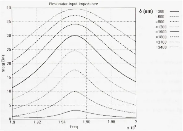
Figure 3.3 Magnitud e of input impedance vs frequency fo r different value s of 8 5 0
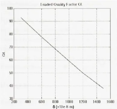
Figure 3.4 . Q i vs 8 5 1
Figure 3.5 Secon d order filter using AJAtS resonators in symmetric feed configuration 5 3 Figure 3.6 Typica l response for the symmetric feed point filter 5 3 Figure 3.7 Effec t o f X on Transmission (a). Adaptation (b) and Zero location (c) 5 5 Figure 3.8 Effec t o f 8 on Transmission (a). Adaptation (b) and Zero location (c) 5 6 Figure 3.9 Secon d order filter usingA./4±8 resonators in asymmetric feed configuration 5 7 Figure 3.10 Typica l response for the asymmetric feed point filter 5 7 Figure 3.11 Effec t o f 8 on Transmission (a). Adaptation (b) and Zero location (c) 5 8 Figure 3.12 Effec t o f 8 on Zero location showing an unresolved zero 5 9 Figure 3.13 Effec t o f X on Transmission (a), Adaptafion (b) and Zero locafion (c) 6 0
Figure 3.14 Firs t iteration of topological opfimisafion 6 4
Figure 3.15 Transmissio n and return loss response of the topology in Figure 3.14 6 4 Figure 3.16 Respons e of the filter in response to parameters sweep 6 5
Figure 3.17 Geometricall y optimized stmcture 6 5
Figure 3.18 Transmissio n and return loss response of the topology in figure 3.17 6 6
Figure 3.19 3 Dimensional model in EMDS 6 7
Figure 3.20 Momentu m (2.5D) vs EMDS (3D) simulafion results 6 9 Figure 3.21 (Right ) the mesh used (Left) the poynting vector distribution at 1.96GHz 6 9
Figure 3.22 Filte r topology with modified port s 7 0
Figure 3.23 Filte r response to variation of port width (Y) for the topology in figure 3.22. ...71 Figure 3.24 Filte r response of the topology in figure 3.22 7 1
Figure 3.25 Classica l duplexe r stmctur e 7 2
Figure 3.26 Topologicall y optimize d duplexe r stmctur e 7 3
Figure 3.27 Optimise d duplexe r response (Left) Retur n loss, (Right) Transmission 7 3
Figure 3.28 (Left ) Filte r (Right) Duplexe r 7 6
Figure 3.29 Filte r measurements (Transmission ) 7 6
Figure 3.30 Filte r measurements (Retur n los s 7 7
Figure 3.31 Duplexer , Transmission (a) . Isolation (b ) and Retu m los s (c) 7 7
Figure 3.32 UMT S filters topologies . (Left) Tx-filte r (Right ) Rx-filte r 7 8
Figure 3.33 UMT S Tx- filter fabrication . Transmission (a) , Retum los s (b) 7 9
Figure 3.34 UMT S R x filter fabricatio n Transmissio n (a) , Retum los s (b) 7 9
Figure 3.35 UMT S duplexe r topology 8 0
Figure 3.36 UMT S Duplexe r fabricafion: Transmissio n (a) , Isolafion (b ) Retum los s (c). ...80
Figure 4.1 Preliminar y coupled resonato r filter o n MMIC substrat e 8 3
Figure 4.2 Electromagnefi c simulatio n results of geometry presented i n figure 4.1 8 4
Figure 4.3 Filte r design guide window 8 6
Figure 4.4 Synthesise d ellipti c 3rd. order filter 8 6
Figure 4.5 Optimisatio n o f a filter section includin g transmission line s Q model 8 8
Figure 4.6 Layou t of an optimised filter sectio n 8 9
Figure 4.7 UMT S Tx band lumpe d elemen t filter 9 0
Figure 4.8 UMT S Tx band lumpe d elemen t filter- simulatio n result s 9 1
Figure 4.9 UMT S R x band filter 9 1
LIST O F ACRONYM S
ADS Advance d Desig n Syste m
BAW Bul k Acoustic Wav e
BiCMOS Bipola r Complementary Meta l Oxid e Transisto r
CPW Coplana r Wav e Guid e
FDD Frequenc y Division Duple x
GaAs Galliu m Arsenid e
GSM Globa l Syste m fo r Mobil e communicatio n
HBT Hetero-juncfio n Bipola r Transisto r
LNA Lo w Noise Amplifie r
LTCC Lo w Temperature Co-fire d Ceramic s
MHMIC Microwav e Hybri d Monolithi c Integrate d Circui t
MMIC Microwav e Monolithic Integrate d Circui t
MS MicroStri p
PA Powe r Amplifie r
pHEMT pseudomorphi c Hig h Electro n Mobilit y Transisto r
RF Radi o Frequenc y
SAW Surfac e Acousti c Wav e
TDD Tim e Division Duple x
UMTS Universa l Mobil e Telecommunication Syste m
On th e roa d t o ubiquitou s connectivity , th e wireles s telecommunicatio n industr y i s witnessing a n unprecedente d deman d fo r multi-mod e multi-servic e wireles s use r terminals . As manufacturer s tr y t o fulfil l thes e demands , majo r challenge s aris e causin g a n eve r increasing difficult y i n thi s endeavour . Whil e manufacturer s ar e increasin g th e numbe r o f circuits integrated int o a terminal, the y ar e faced wit h th e insatiable deman d o f the consume r to have lighter, smaller , an d cheaper terminals .
On th e other side , the coexistenc e o f a multitude o f wireles s standard s necessitate s excellen t management o f the radio frequency resource s an d isolation between differen t radi o frequenc y bands.
Radio frequenc y filters an d duplexer s ar e th e come r stone s i n spectra l management , havin g escaped miniaturizatio n trend s fo r a relativel y lon g time ; nowaday s the y ar e a t th e centr e stage o f thes e trends . A s th e telecommunicatio n industr y i s experiencin g it s highes t growt h rates i n th e mobil e sector , wher e th e frequenc y band s allocate d fo r thes e service s ar e typically i n th e lowe r en d o f th e microwav e frequenc y ranges , miniaturisatio n i s no t a goo d to have feature , i t becomes a pressing necessity. The difficulties encountere d i n miniaturisin g these component s stem s fro m som e fundamenta l physica l an d technologica l limitations . These limitation s ar e challengin g researcher s t o pus h th e limit s o f desig n technique s o r fabrication technologie s o r both.
Our work subscrib e t o this general effor t o n the design techniqu e front . Th e design techniqu e chosen i s tha t o f topologica l optimisatio n t o desig n miniatur e couple d resonato r filters i n Microstrip stmctures . I t ha s th e advantag e tha t i t ca n benefi t from man y o f th e fabricafio n technologies advancemen t i n the fijture.
14
Organization
The thesi s i s organized a s follows ; i n Chapte r 1 we will presen t a system overvie w o f th e filters and duplexers in the context of multimode wireless systems. Then we introduce planar coupled resonators filters as a candidate approach fo r designing miniaturized R F filters. The system characteristics of these filters are explained followed b y an introduction to the design parameters o f these filters; thos e being, quality factor , coupling , and extema l qualit y factor . We conclude by a literature survey of the state of the art, followed b y a brief comparison of the results reported by different desig n approaches in open literature.
Chapter 2 will serve as a theoretical introductio n fo r the design o f coupled resonato r filters. We start with the introduction of direct coupled resonator filters and how to they synthesised from low pass prototypes, then a theoretical introductio n of the transmission zeros , and how they are realised using coupled resonator.
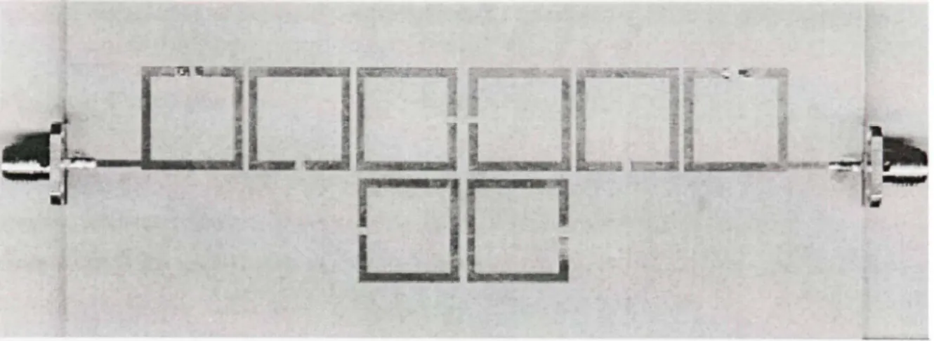
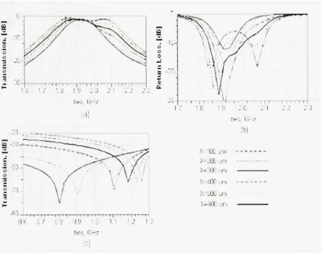
In Chapte r 3 w e wil l presen t th e techniqu e employe d t o desig n miniaturize d filters an d duplexers. W e star t b y presentin g th e /l/4±< 5 wavelengt h resonato r whic h i s th e basi c resonator i n ou r work . Subsequently , th e resonato r wil l b e use d t o desig n tw o filtering stmctures, the symmetric feed and the non-symmetric feed. Using computer aided design and analysis we will compare the two stmctures to choose a candidate for miniaturisation. Onc e we hav e a candidat e stmctur e w e wil l appl y th e topologica l optimisatio n techniqu e t o miniaturise th e filter. Finall y w e wil l presen t th e measuremen t o f filters an d duplexer s fabricated vi a MHMIC process.
In Chapter 4 we will present the results of filters designed usin g the technique introduced in chapter 3 and lumped elements ; both are designed targetin g a high end MMI C process. The target process is called TQPED. This MMIC process of TriQuint Semiconductors is a process where typically several elements of the RF front (ex. LNA, PA) end can be integrated.
1.1 Introductio n
Filters an d Duplexer s ar e integral component s i n virtually all wireless fron t ends . A typical architecture o f a multimode fron t en d i s presented i n figur e 1.1 . The architecture presente d integrates Frequenc y Divisio n Duple x -FD D (ex : WCDMA ) syste m wit h Tim e Divisio n Duplex-TDD (ex : GSM) . I n FD D system s transmission-receptio n (Tx-Rx ) separatio n take s place i n th e frequenc y domain , thi s impose s constrain s o n the filtering elements ufilise d i n the front-en d an d necessitates th e use of a duplexer fo r frequenc y separation . Whil e Tx-Rx separation in TDD takes place in the time domain, the RF front-end filters are still required to have stron g attenuatio n characteristics . Anothe r importan t distinctio n betwee n TD D an d FDD systems lies in the source of interference. Whil e in TDD systems the major interferer s lay outside the wireless device, in FDD systems interferers la y inside the module as leakage between the TX and RX paths in the front end .
In RF front-ends, divers e an d often opposin g requirements o n different component s ten d to make the integration o f all RF components using a single fabrication technolog y a challenge that prove d resilien t t o definitiv e solutions . Consequently , manufacturer s us e differen t integration technologie s to be able to meet required leve l of performance withi n the allowed area fo r eac h devic e simultaneously . Th e powe r amplifie r fo r exampl e i s usuall y manufactured o n a GaA s HB T (Galliu m Arsenid e Heter o Junctio n Bipola r Transistor ) processes, a fabrication technolog y which provides good thermal characteristics that suits this component th e best . Th e Mixe r an d LN A (Lo w Nois e Amplifier ) ca n b e integrate d int o a single chip using a SiGe BiCMOS (Silicon-Germanium Bipola r Complementary Metal Oxide Transistor) proces s wher e lo w nois e an d goo d linearit y ca n b e achieved . Furthermore , a
16
significant effor t ha s bee n pu t t o integrat e thes e module s i n a syste m o n packag e styl e providing excellent performance and miniaturization.
Unfortunately, antennas , filters and duplexer s have largely eluded thes e miniaturizatio n an d integration trends . Filters an d duplexer s ar e high Qfacto r passive s o f relatively larg e size -measured i n term s o f th e guide d wavelength - the y ar e mostl y extema l component s t o th e other integrated circuits in the front-end.
Different solution s have been proposed for the design of miniaturized high-Q passives for RF fronts ends . Th e mos t popula r o f whic h i s usin g acousti c wav e technologies , thes e hav e found suppor t fro m equipmen t manufacturer s a s acousti c wav e filters quickl y becam e th e industry de-fact o technolog y fo r miniaturize d filters. Therefore , SA W (Surfac e Acousti c Wave) an d BA W (Bul k Acousfi c Wave ) ar e foun d i n ever y use r terminal . A majo r disadvantage o f thes e filters i s tha t thei r fabricatio n proces s i s incompatibl e wit h thos e o f other component s o f th e fron t end , als o lo w powe r handlin g capacity ; stabilit y an d a relatively hig h insertio n los s ar e als o concems . Fabricatio n proces s incompatibilit y o f acoustic wave devices stems from th e characteristics of their fabrication processes ; for SAW filters, fragility an d the need of hermetic packaging inhibits their monolithic integration with active component s [1] . On the other hand BA W filters have mechanical characteristic s tha t are more integration friendly , bu t th e materials used and the fabrication constraint s required for BA W fabricatio n ar e largel y differen t fro m th e standar d activ e device s fabricatio n process such that monolithic integratio n result s in a more expensive, lower yielding process, therefore, monolithic integration of BAW integration is disadvantageous[l].
Antenn;i
L/
RF BP F GSM1900 V L N Ap ^
Power Amplifie rP-
V L N A V L N A Power Amplifie rP-
V L N A —I?-LO -ir-L O GaAs HB T IFigure 1.1 ^ multi-mode front end module with emphasis on integration technologies.
Researchers have dedicated a lot of attention to planar filter and duplexer miniaturization in recent years owing to their ease of fabrication, seamles s integration potential, power handling capability, stability and cheap price.
This renewe d interes t fo r technologie s suc h a s MHMI C an d MMI C hav e produce d significant advance s i n the design technique s o f miniature plana r filters. Plana r fabricatio n processes hav e distinc t advantage s o n other processe s i n terms o f cost, integration , powe r handling an d stability; moreover , thes e processes ar e mature and have prove n t o give high yield in a high volume context. The major disadvantag e of these technologies is the inherent difficulty o f designin g filtering stmcture s tha t accommodat e lo w GH z frequency circuit s having low insertion loss, small fractional bandwidth (<5%), and miniaturized size.
In this wor k w e tackle the miniaturization proble m o f filters and duplexers targetin g thos e fabrication technologie s o f active front-en d component s i.e . LNA and PA, these processe s are fiindamentally planar i n nature o f which MHMI C an d MMIC processe s ar e examples. Our techniqu e i s base d o n a topologica l optimizatio n o f folde d hal f wavelengt h couple d resonators filter.
18
1.1.1 Plana r RF Filters
Planar R F filter s ar e these filters that us e planar stmcture s t o realise th e filtering elements. These filters are typically manufactured a s MicroStrip (MS) or Coplanar Wave Guide (CPW) stmctures, whether distributed or lumped. Distributed planar filters tend to be relatively large due t o th e us e o f resonator s whos e size s ar e comparabl e t o th e wavelength . A t lo w GH z frequencies, th e are a occupie d b y thes e filters inhibit s thei r us e i n man y application s an d eliminates th e optio n o f thei r monolithi c integratio n i n mode m use r termina l front-ends. While lumpe d componen t filters d o no t suffe r fro m th e aforementione d drawback ; thei r power handling capacity and Q factor at high frequencies ten d to be poor.
RF filters use d i n mode m mult i mode/ban d fron t end s ar e predominantly ban d pas s filters with relatively low fractional bandwidth. To design such filters in planar stmctures; coupled resonators technique s ar e widel y employed . Recently , cros s couplin g technique s ar e extensively utilise d t o inser t finite frequenc y transmissio n zero s fo r enhance d skir t characteristics an d reducin g th e numbe r o f resonator s use d i n th e filter; consequentl y reducing the filter size.
The system characteristics of filters that are of concem in the context of this current research are insertion loss, retum loss , attenuation an d relative size. These characteristics are define d as follows:
- Insertio n Los s (IL): Is the loss in signal powe r resulfing fro m th e insertion of the filter in the path of the signal. I t is expressed a s the ratio of the incident power Pi n to its input port to the output power from its output port Pou t i n the pass band of the filter. Thi s quantit y i s measure d i n term s o f th e transmissio n scatterin g networ k parameters (S2 1 an d S12 ) commonl y use d i n vecto r networ k analyzers . Thes e quantities are represented mathematically as:
It is generally required that the insertion loss be kept to a minimum especially in the context of RF front-ends, where less than 3dB are typically accepted values.
- Retur n Los s (RL) : I s the power reflected fro m th e filter as a result o f impedance mismatch betwee n th e source and filter. It is expressed a s the ratio of the incident power Pi n t o it s inpu t por t t o th e reflecte d powe r fro m it s inpu t portP^^f . Thi s quantity i s measure d i n term s o f th e adaptatio n scatterin g networ k parameter s (Sll an d S22) commonl y use d i n vecto r networ k analyzer . Thes e quanfitie s ar e represented mathematically as:
RL=101og(PiJ-101og(P,,,-) (1.2 )
- Attenuation : The attenuation i s a transmission characteristi c of the filter; it can be considered th e insertio n los s i n th e sto p ban d o f th e filter. I t i s measure d b y th e same transmission scattering parameters as the insertion loss. In the context of multi band/mode operafion it is imperative to distinguish two distinct frequency bands.
o Narro w Ban d Attenuation : I t is the attenuation characteristi c o f the filter near th e pass ban d o f th e filter. Thi s attenuatio n usuall y i s specifie d a s a required attenuation leve l at a finite frequenc y whic h in turn determines the required steepness of the filter and consequently the order of the filter.
o Wid e Band Attenuation: It is the attenuation characteristics of the filter up to an d beyon d th e secon d harmoni c o f th e centra l frequenc y o f th e filter. This characteristi c i s very importan t du e to the inherent propert y o f plana r resonant stmcture s t o have repeated an d spuriou s pas s bands harmonic s o f the filter's central frequency . Specia l attention has to be given to assure that the wide band attenuatio n characteristi c o f the filter does not allo w signal s from other modes/bands to interfere with signals of the operafional band .
20
Both o f thes e characteristic s ar e represente d b y th e transmissio n scatterin g networ k parameters (S12 and S21).
- Relativ e Size: In the context of our research we will define the size of the filter as th e minimu m rectangl e require d t o plac e th e filter o n a substrate . Th e rectangle's width and breadth will be measured i n terms of the>ig. Where Xg is defined a s the guided wavelength of a transmission line on the same substrate of the filter. For example a filter may occupy an area of 60mmx20m m whil e the guided wave length could be 11m m ; then the fdter size is 6A.gx2>tg.
1.1.2 Duplexer s
Duplexers ar e passiv e thre e por t device s tha t allo w a singl e antenn a t o b e share d simultaneously b y a transmitte r an d a receive r operatin g i n clos e bu t separat e frequenc y bands. Th e ports of a duplexer are transmission port , reception port, and an antenna port as depicted in Figure 1.2 .
In th e contex t o f mode m multimod e FD D fron t ends , efficien t utilizatio n o f th e availabl e bandwidth require s guard bands to be relatively small . Moreover , du e to the large dynamic range between the transmitted signal and the received one - typicall y more than 70 dB - i t is required tha t th e duplexe r provid e stee p separatio n betwee n th e tw o band s fo r prope r fiancfionality o f the system and efficient bandwidt h utilisation. I t is worth noting that in FDD systems th e noise i s intemally generate d from th e system; sinc e there ar e two differen t R F signals propagating through the system.
Antenna Matching Network A/4 P2 T o Reciever
Figure 1. 2 Duplexer architecture.
Duplexers ar e made o f two band-pass filters; on e connect s t o the transmitter an d th e other t o the receiver , eac h o f these port s i s a port o f th e duplexer . Th e othe r tw o port s - one o f eac h filter - ar e separate d b y quarte r wav e transmissio n lin e an d a matchin g networ k connectin g the third outpu t por t of the duplexer to the antenna .
The syste m characteristic s o f duplexers o f conce m i n the context o f this current researc h ar e insertion loss , retum los s an d isolatio n an d relativ e size . These characteristic s ar e defined a s follows:
- Insertio n Los s (IL) : The insertio n los s o f th e duplexe r i s define d similarl y t o tha t of the filter. Th e only difference i s that duplexers have two distinct pas s bands; on e for th e transmission , th e othe r fo r th e reception . Th e Insertio n los s fo r th e transmission ban d i s commonl y require d t o b e abou t Id B les s tha n tha t o f th e receiving band .
- Retur n Los s (RL) : The retum los s of the duplexer i s defined similarl y to that of the filter. Th e onl y differenc e i s tha t duplexer s hav e tw o distinc t pas s bands ; on e fo r the transmission, th e other for the reception .
9?
- Isolation : I t i s th e relativ e attenuatio n provide d betwee n th e tw o path s o f th e
duplexer; transmitte r t o antenn a pat h an d antenn a t o receiver path . A s w e indicate d before thi s characteristic i s of fundamenta l importanc e i n the syste m becaus e o f th e large dynamic between th e transmitted signa l an d the received one .
o T x i n R x band : I t i s th e attenuatio n provide d b y th e duplexe r fo r a signa l having a frequenc y equivalen t t o tha t o f th e receptio n ban d whe n injecte d from th e transmission por t of the duplexer.
o R x i n T x band : I t i s th e attenuatio n provide d b y th e duplexe r fo r a signa l having a frequency equivalen t t o that of the transmission ban d whe n injecte d from th e reception por t o f the duplexer .
1.2 Surve y of pertinent researc h activitie s
Miniaturization effort s followe d differen t approache s o n bot h th e fabricatio n an d th e desig n front. Sinc e w e ar e primaril y conceme d wit h th e desig n aspect s o f miniaturization , w e wil l present here the most pertinen t approache s followe d b y different researc h team s in this field. A direc t approac h fo r achievin g highly miniaturized filters i s to use lumped components ; thi s achieves miniatur e filters bu t suffer s ver y poor performanc e i n terms o f losse s an d steepnes s of attenuation whe n standar d processe s ar e employed. Th e origin o f this poor performance i s mainly tha t th e qualit y facto r o f inductor s an d capacitor s deteriorate s rapidl y a t radi o frequencies. Mode m MMI C proces s ca n achiev e hig h qualit y facto r (>500 ) fo r capacitors , but quality factor s fo r inductors remain ver y limited whe n using finite conductivit y metals. In [2] Hig h Temperatur e Superconductor s (HTS ) wer e use d t o realis e a 3'^'' . orde r bandpas s lumped element s filter, th e use o f HT S materia l allowe d fo r th e realisatio n o f inductors wit h high qualit y factors . Whil e result s reporte d i n [2 ] ar e satisfactor y i n performanc e an d miniaturization, th e filters us e uniqu e material s an d fabricatio n proces s tha t ar e no t directl y
compafible with commercially available MMIC process; moreover, the use of HTS requires a cooling mechanism for materials to maintain their superconductive properties.
Another altemafiv e t o overcome inducto r losse s whe n designin g lumpe d component s filters is to use Q-enhanced or active inductors as suggested in [3]. This technique increases slightly the are a o f inductor s use d i n th e desig n bu t allow s fo r arbitrar y Q-factor . Problem s o f impedance matching between active and passive components, non linearity and stability tend to limit the application o f these filters to IF frequency ranges. Furthermore, in the context of RF front ends , powe r efficienc y i s a majo r conce m fo r batter y operate d use r terminals ; consequently the use of active components is not suitable.
A differen t approac h fo r filter miniaturizatio n ha s bee n develope d aroun d hair-pi n filters. Hairpin filters ar e classica l couple d resonato r filters. Th e s o calle d Hairpi n stmctur e i s considered a folded for m of half-wavelength transmissio n line resonators.
In [4] the arms of Hairpin resonator were folded fo r the purpose of filter miniaturization an d direct couplin g wa s used t o produce a third orde r miniatur e filter. Further development s i n [5] introduced stmctura l improvemen t to the hairpin resonator and cross coupling techniques were introduced to provide a miniature and highly selective filter.
Finally, i n [6] the filter introduced i n [4 ] was realised using multilayer inte r coupling on an LTCC (Low Temperature Co-fired Ceramic ) process. This technique has produced excellen t miniaturization result s fo r a fou r quasi-ellipti c ban d pas s filter, bu t losse s wher e relativel y high fo r meta l thicknesse s accessibl e usin g thi s technology , als o som e divergence betwee n the electromagneti c simulatio n an d th e measurement s obtaine d du e t o th e difficultie s o f simulating th e mult i laye r inte r coupling . Despit e thes e problem s thi s techniqu e promise s very high miniaturization potentia l an d coul d prov e to be very successfril. I t is worth notin g that thi s technique ca n be utilized t o further miniaturiz e th e filters we developed, providin g additional miniaturization for our filters.
24
Moreover, anothe r approac h i s t o us e dua l mod e resonators . A dua l mod e resonato r i s a resonator that i s designed to excite high order modes and recombine them at the output port. These modes have slightly different resonan t frequencies whic h allows for the design of band pass filters. Th e miniaturizatio n aspec t stem s from th e fac t tha t onl y a singl e resonato r i s required t o desig n a filter. Good miniaturizatio n ca n b e achieve d usin g thi s technique s bu t due to the sensitivity o f the excited mode s to the symmetry of the resonator, th e size of the resonator remain s large r tha n mult i resonato r filters designed b y alternative techniques . An example of a miniaturized filter of this type is a fractal dua l mode filter presented in [7].
Finally, anothe r approac h fo r filter miniaturizatio n i s t o find a miniatur e topolog y wit h minimal Ohmic losses. In [8] a new methodology for topological compacting was introduced, also a se t o f filters and a duplexer fo r UMT S front en d wa s designe d an d fabricate d o n a standard alumin a substrate . Th e filters an d th e duplexe r reporte d hav e achieve d hig h performance an d compac t size . Thes e ar e th e mos t miniatur e filters t o ou r knowledg e i n single layer Microstrip stmctures.
After w e have reviewed the different approache s in designing planar filters, we will present a comparative table to compare the respective performance of each of these techniques.
Table 1. 1
A comparative table between the different approache s
Approach
Lumped Components (HTS) Hairpin multilayer
Dual Mode Resonators (Fractal) Topological Optimizatio n Fractional Bandwidth 0.844% 3.7% 1% 2.5% Attenuation -60dB -30dB -50dB -45dB Size 10mmx3.5mm 5x7mm0.16X0.11 20mmx20mm 0.15X0.15 9mmx7.5mm 0.125X0.15 Central Frequency 1.7GHz 3GHz 0.85GHz 2GHz
From th e tabl e abov e w e ca n witnes s tha t th e topologica l opfimisafio n techniqu e achieve s high performanc e an d excellen t miniaturisation , fo r thi s reaso n i t wa s chose n fo r furthe r investigation i n our work . I t is our goa l t o reproduce th e same performance reporte d i n the above references, bu t non e the less to improve o n the miniaturization an d simplicit y o f the topology used.
1.3 Conclusio n
In this chapter we presented R F filters and duplexers in the context of modem RF front-ends. It is evident that with multimode/multi band requirements the number of RF filters is on the rise. Thi s constitute s a fundamenta l thms t behin d miniaturizatio n an d integratio n efforts . These effort s ar e considere d a n enablin g elemen t fo r th e futur e o f th e persona l telecommunication revolution . Th e reasons behin d th e interes t fo r developin g miniaturize d planar filters were discussed an d a review o f the most mature approaches i n this filed were presented. Finall y a resum e o f th e result s reporte d i n literatur e usin g th e presente d approaches establishe s th e viabilit y o f th e topologica l optimizatio n techniqu e fo r furthe r research. I n chapter 2 we will present a theoretical back groun d fo r the principal technique s for the design of planar coupled resonator filters.
CHAPTER 2
PRINCIPLES OF COUPLED RESONATORS FILTE R DESIGN
2.1 Introductio n
In thi s chapte r w e ar e conceme d wit h buildin g a knowledge bas e o f th e som e o f the mos t fundamental an d widely used concepts in coupled resonator s filter design. We start with the general theor y o f direc t couple d resonato r filters an d thei r synthesi s fro m lo w pas s prototypes, then we will us e general filter theory of lumped elemen t technique s to illustrat e the concept of transmission zeros at finite frequencies. Subsequently, we will explain how in
direct couple d resonato r topologie s ar e use d t o realis e transmissio n zero s a t finit e
frequencies.
2.2 Desig n of direct coupled resonator band pass filters
Direct couple d resonato r filters i n thei r mos t elementar y for m coul d b e represente d a s i n Figure 2. 1 below . Al l resonator s ar e identica l an d ar e directl y couple d t o on e anothe r a s depicted in the figure. Th e value of the coupling coefficient i s denoted byA/„ „^| an d can be positive or negative. Coupling between non adjacent resonator s is neglected. The coupling to the extemal port s i s denoted b y the extemal qualit y factor^g . Coh n i n [9 ] has introduced a method fo r designing couple d resonator s bandpass filters from lowpas s prototypes. Late r in [10] he applied hi s method t o design a multitude of different stri p line parallel transmissio n line resonators. The method i s based o n a theoretical derivatio n o f an equivalent circui t fo r microwave couple d resonator s suc h tha t th e couplin g betwee n resonator s act s a s a n idea l immittance inverter.
Q e M,, 2
n/ \
M3.4Rin: H H
1]
Ht-n Hl-i r"! H h H H HHiM, -Direct Couplin g
Figure 2.1 A general representation of direct coupled resonators filter.
The goa l o f Cohn' s metho d i s t o establis h a relatio n betwee n th e circui t parameter s o f a prototype filter an d th e couplin g parameter s o f th e microwav e resonator s arrangement , i.e. , the couplin g coefficientsM „ „^] , an d th e extema l qualit y factor^^ . Disha l i n [11 ] ha s described a n experimenta l metho d fo r findin g th e couplin g coefficien t an d th e extema l quality facto r o f couple d resonators . Thi s metho d ca n b e adapte d t o wor k i n th e contex t o f modem electromagneti c simulatio n technique s instea d o f measurements . Therefore , usin g the combination o f Cohn's formulatio n an d DishaFs technique we can design bandpass filters from lowpas s prototypes wit h relatively little effort .
It is important befor e furthe r detai l t o mention tha t ther e ar e different qualit y factor s tha t ca n be associated wit h circuit . Hence , it is important t o discuss the m an d t o identify th e qualifie s they measure a s well a s the relation between them .
A qualit y facto r i s a ratio betwee n energ y storag e an d energ y los s i n a resonator. Dependin g on the origin of the losses being considered on e can define thre e quality factors [12] :
Unloaded Q: Q,=( o _ Energ y stored i n theresonant circui t
Extemal Q : QE= M
Power los s in the resonant circui t Energy stored i n the resonant circui t
Power los s in the extemal circui t
(2.1)
28
Loaded Q: Q , =o) Energy stored in the resonant ircuit Total power loss
These three factors are related by the following equation :
_L-_L J _
(2.3)
(2.4)
In the planar filter design context we are more concemed with the extemal qualit y factor Qe, as the unloaded qualit y factor Qu has an upper limit that can not be surpassed for a particular fabrication technology . Also, it is very common that the values of Qe required for realizing a filter is much lower than that of Qu; and consequently becomes more dominant.
In thi s sectio n w e wil l explai n i n som e detai l ho w t o deriv e th e equivalen t circui t a s pe r Cohn's method . The n w e will illustrat e ho w DishaF s metho d wa s adopte d t o calculat e th e coupling coefficients usin g electromagnetic simulation.
2.2.1 Derivation of the equivalent circuit
Electric networ k circui t solution s ar e ver y wel l establishe d an d circui t capacitanc e an d inductance values have closed for m solution s for Chebychev and maximally flat type filters. The startin g poin t i s th e lowpas s filter prototyp e show n i n Figur e 2. 2 wher e th e circui t parameters ^'^.s , , « ^j-g t^g capacitances and inductances values as given by the tables for the n-even or n-odd filters. Th e value of r is generally taken to be unity except for the n-even fo r Chebychev responses . Thes e value s ar e availabl e i n virtuall y al l reference s treatin g filter design of which [13] is an excellent example.
g?_
J171
93 J 9 4 L _ 1 Qn-r l 9n-7JXl
Figure 2.2 Low pass prototype filter of Chebychev or maximally flat response.
To transfor m th e lowpas s prototyp e t o a bandpas s filter w e us e th e lowpas s t o highpas s transformation show n in Figure 2.3.
LP to BP Transformation
R_
6
Sc gLA is the fractional bandwidt h o f the filte r
(Ofj i s the central frequency o f the filter
(^OSL
SL
a)„A
Figure 2.3 Lowpass to Highpass Filter Transformation.
Applying thi s transformatio n t o th e lowpas s prototyp e yield s a bandpas s filter wit h th e corresponding bandwidth , centra l frequency , an d attenuatio n characteristic s a s illustrated i n Figure 2.4
Bandpass filter trasnformed from lowpass prototype 30 rem rrm rem
]i
>' L , = rrm ^ L „Figure 2.4 Trasnformed bandpass filter (Bottom) Circuit transformation.
In order to transform th e band pas s filter to a form tha t approximate s tha t of figur e 2.1 , we need t o get rid of the parallel arm s of the filter. Consequently, th e next ste p is to transfor m the bandpass filter to an equivalent circui t with only series or parallel resonator sections and immittance transformers . Immittanc e transformer s allo w th e transformatio n o f a serie s section to a parallel section and vice versa [7].
Impedance inverters Admittanc e inverters
57 K ±90° 0 T ''I J ±90°
i
1
r.-y-Figure 2.5 Conceptual operation of immittance inverters.
The conceptua l operatio n o f immittanc e transformers , als o calle d inverters , i s illustrate d i n Figure 2.5. I t was demonstrated by Dishal in [11] that these immittance transformers ca n be
realized usin g electromagneti c coupling . Usin g thes e circui t transformatio n an d electromagnetic couplin g a s immittance transformers w e obtain the required for m o f the filter depicted i n figure 2.1. 3H'::iiiiiii"C~ Ai:5=-'53re$*n3!"r5efy
kc,
y^ +1 ^tfl ^. ^ i:L,
'1+1-y,
J+2 •1+1H4
+90P
J " ^41 C m tj+ j '1+2ianSDrij sec:D' inDe:£"t Ka-c.
J'"'"'
i+i
Vc
1+1 "i •^ i . T Y 1+2Figure 2.6 Step-by-step band pass section transformation
Figure 2. 5 illustrate s th e ste p b y ste p ban d pas s sectio n transformation , wher e Li,C i ar e th e inductance an d capacitanc e o f the i ' Secfio n o f the filter , Yj+ i is the inpu t admittanc e o f th e i"^-i-l sectio n o f the filter afte r impedanc e scaling. Finall y Y"i and Z'j ar e the input admittanc e and impedanc e respectively of the final transformed section .
The first ste p i n th e transformatio n i s t o scal e th e impedanc e o f th e i" ^ bandpas s sectio n t o have the same series resonance arm a s the all serie s resonator section s as illustrated i n Figur e 2.6. Thi s require s tha t al l th e othe r filter coefficient s b e als o impedanc e scaled . I t i s t o b e
32
noted tha t Lj , C j ar e th e value s afte r transformatio n an d L; , C j ar e th e origina l bandpas s filter values . Fo r these sections to be equivalent th e following conditio n mus t b e safisfied :
^i+\ - ^ j + i
Expanding this condition yields :
<^i+i - 0)1 L
i +1 J Li ^+y..2=—. K I 4 + 1 (oL i+\ o)C i+\ J + '^,^2
(2.5) (2.6)
After identifyin g th e quantitie s tha t hav e th e sam e dependenc e o n co [9 ] an d usin g th e transformation identitie s i n Figure 2.3 we find:
K i ,i +1 A L,L„, (2.7)
fQ\S,gi+\
The sam e procedur e fo r th e first an d las t section s o f th e couple d resonato r filter yield s th e expression fo r th e extema l qualit y factors . Moreover , i t i s a general practic e tha t resonator s used in the design ar e identical. Consequentl y the following form s ar e generally preferred :
a. -i^..
^,-,/+l= —
(2.8) (2.9) /o V^/^<+l
These formula s relat e th e normalise d couplin g coefficien t t o a lowpas s prototyp e suc h tha t the ripple an d th e attenuatio n respons e o f th e filter ar e preserved . I t i s t o b e note d tha t thi s method achieve s goo d result s onl y fo r lo w t o moderat e fractional bandwidt h bandpas s filter because i t completely neglect s the dependence o f the coupling coefficient o n frequency. Th e utility o f these equation s i s not directl y relate d t o an y particular resonator , consequentl y an y arbitrary resonato r ca n b e use d t o realis e th e filter. T o realis e th e require d filter i t i s
necessary t o b e abl e t o achiev e th e couplin g coefficient s value s require d b y th e equation s above. Th e couplin g i s mainl y dependan t o n geometrica l parameter s an d i s determine d b y either experiment and/o r electromagneti c simulatio n a s explained i n the following section .
2.2.2 Extractio n o f coupling coefficients usin g electromagnetic simulatio n
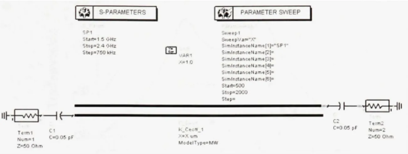
The couplin g coefficient s betwee n resonator s M, ,+, , th e extema l qualit y factor^,, , an d th e unloaded qualit y facto r ^ „ ar e the only parameters a designer i s required t o know i n order to realise a bandpass couple d resonato r filter a s w e hav e previousl y illustrated . Onc e th e basi c resonator i s chosen , th e unloade d qualit y facto r ^ „ i s fixed an d i s mainl y controlle d b y th e fabrication technolog y parameter s suc h as ; meta l conductivity , substrat e los s tangent , an d metal thickness . Consequently , th e desig n parameter s o f interes t ar e Q^ and th e couplin g coefficients M , , + i . I n [11 ] a detaile d method , referre d t o a s DishaF s procedure , fo r measuring thes e parameter s i s presented . I n thi s sectio n w e ar e conceme d wit h th e application o f this method usin g ADS/Momentum electromagneti c simulatio n [14] .
The setu p fo r measurin g th e couplin g coefficient s betwee n tw o half-wavelengt h Microstri p resonators i s shown i n Figure 2.7. Th e method call s fo r detectin g the amplitude respons e t o an excitation fro m a source that lightl y load s the resonator (i.e . decrease the unloaded qualit y factor b y les s tha n 10%) . Fro m th e amplitud e respons e th e couplin g coefficien t an d th e extemal qualit y facto r ar e calculate d b y recordin g th e peaks , th e frequency differenc e between thes e peaks , an d th e fractiona l bandwidt h o f th e response . Consequently , fo r different value s o f th e geometrica l parameter s X an d 5 on e ca n calculat e bot h coefficient s for an y desired configuration . W e will carr y out thi s procedure vi a ADS\Momentu m usin g a co-simulation technique . Th e co-simulatio n techniqu e permit s th e simulatio n o f circui t elements, lumpe d o r distributed , an d distribute d layou t component s simultaneously . Th e layout component s ar e simulate d vi a electromagneti c simulatio n an d th e circuit s ar e
34
simulated base d o n thei r respectiv e circui t models . Usin g thi s techniqu e a parameterize d layout o f th e couple d resonator s wa s buil t an d ver y lo w lumpe d capacitor s wer e use d t o lightly couple the ports of the resonators.
Matched Sourc e Lightly Couple d Source Coupled Resonators Detector Lightly Couple d X \ ^
Lightly Couple d Detector
Figure 2.7 (Left) Setup for Q^ measurement (Rigth) Setup for K measurement 2.2.2.1 Extractin g of coupling factor M
The circui t i n Figur e 2. 8 i s use d t o calculat e th e couplin g coefficien t M between th e resonators for different value s of the distance X betwee n them.
III-7 —vw Term I Hum=1 Z=50 O h m C 1 0=0 0 5 p F ^^ SP1 S-PARAMETERS Stdrt=1 5 OH z Stop Step =2 4 CH z = 750 kH z
1
E ] /.= 1 0 K_Ctc-ff_1 X = X u m Mo del Type ^% PARAMETER SWEE P 1 i.Krepl S'AieepVdf="X" SirnlnstanceN3rne(1]="SPr' ?imlnstariceNarTie{21= Simlni1anc€N3me[JI= SirrilnstariceH3rTie[4]= 91 fTi! n^t a n ce H J m e [5]= SirTilri<1flnceHjrTi«[61= Stjrt=500 Stop=2000 Step= = MW C=0 05 p F AAA^7H|I Num=2 Z=£0 O h mFigure 2.8 Circuit co-simulation for determining coupling coefficient.
The results of the simulation ar e presented i n Figure 2.9 below. B y inspection w e can find that the central frequenc y /gi s 1.85GHz . Als o we can note the frequencies of the peaks on the response for different value s of X an d we designate /;, to the higher frequency an d // t o the lower frequency o f the response's peaks. Th e coupling coefficient ca n then be calculated as follows:
M = fh ~fl /o
The following table summarises the results for the different value s of X. Table 2.1
The values of the coupling coefficient M Separation A' (/jm ) Coupling Coefficient M 500 0.0784 1000 0.0346 1500 0.0162 (2.10)
36 c o </>
"E
(/) c ^.I--20
X(um) = 500 X(um)=1000 X(um)=1600 I ' I ' I ' I ' M 1 ' I ' I I 1 ' i ' 1 ^ •^•vJ-vJ-^-vJC»O0O0O0O0O0O0O0O0C»CDCDCD(DCDCD c n a ) - - j o o ( D O - ^ K ) c o . ^ c n c D - ^ o o ( D O - » - N J C O - u c nfreq, GHz
Figure 2.9 Extracting of the coupling coefficient between two resonators. 2.2.2.2 Extractin g of external quality factor^^
The circui t presente d i n Figur e 2.1 0 belo w i s use d fo r th e determinatio n o f th e extema l quality factor, whereb y we note the peak and the 3dB frequencies o n the transmission curv e of Figure 2.11. W e then apply the following equation to find the required values.
Qe = / o
The results of applying the above equation are presented in the Table 2.2. Table 2.2
The values of the couplin g coefficient Q^
S (^m) Qe 16000 124 16500 78 17000 47 (2.11)
©
S-PARAMETERS 1 S Parar n SPl Start=1.5GHz Stop=2 4 GHz Step= /AR VAR1 d=10 ^% PARAMETER SWEE P ParamSweep Sweep 1 SweepVar="ij" SimlnstariceName[1]="SPl" jg^^ SimlristanceHame[2] = -[-pi-PPl SimlnstanceName[3] = Mum=1 SimlnstanceMame[4] = Z=50 Ohm SimlnstanceName[5] = SimlnstariceName[6]= C Start = 12000 CI Stop= l C-0 05pF Step= l Res_Coupling_Qe Res_Coupling_Qe_l cl=12000um ModelType=MW^1
- j ^
^ Ter m ^2 Term 2 C=0 05pF ^j,m= 2 Z=50 OhmFigure 2.1 0 Circuit Co-simulation for determining external quality factor.
-20-c o l/> </) F (/) c (0 1-•25^ - 3 0 ^ •3fa--40 1 — I — I — I — I — I — I — I — I — I — I — I — I — I — I — I — I — I — I — I — I — I — r 1.84 1.8 5 1.8 6 1.8 7 1.8 8 1.8 9 5 (urn) = 16000 5(um) = 16500 5 (urn) = 17000 freq, GH z
38
2.2.3 Transmissio n zero s at finite frequencie s
Direct couple d resonator s filter s ar e ver y versatile an d relativel y simpl e t o design . Despit e their attractiv e features , thes e filters ca n onl y realis e Chebyche v pas s ban d characteristics . When these filters are used at relatively low frequencies an d high selectivity is required, the size an d losse s ten d t o be ver y prohibitive . A wa y t o realis e highl y selectiv e filters i s t o design filters tha t achiev e transmissio n zero s a t finite frequencies. Thes e filters have hig h selectivity wit h lowe r filte r order , an d constitut e a ver y interestin g altemativ e fo r hig h performance band pass filters.
A transmission zer o occur s i s whe n n o transfe r o f power betwee n th e sourc e an d th e loa d takes place. Chebyche v ban d pas s filters, whether the y ar e based o n lumped o r distributed components, achieve their zeros at infinite an d zero frequency. I n Figure 2.12 a Chebychev band pas s filter circuit i s represented a t infinite frequenc y an d a t zero frequency . Fro m the figure w e ca n not e tha t th e C2, LI , an d L 3 provide a transmission zer o a t zero frequency , while CI, L2, and L4 provide a transmission zero at infinite frequency . Also , we note that a 3"* orde r Chebyche v filter wil l provid e a n equa l numbe r o f zero s a t zer o an d infinit e frequencies.
Elliptic filters , o n th e othe r hand , ar e a famil y o f filters tha t achiev e transmissio n zer o a t finite frequencies , givin g the m thei r superio r attenuatio n characteristics . Ellipti c filters are similar t o Chebyche v filters i n tha t the y ar e equirippl e i n th e pass band , bu t the y ar e als o equiripple i n th e sto p band . A compariso n betwee n th e amplitud e respons e o f 3'^' * order ellipfic and Chebychev filters is presented in figure 2.13.
Elliptic filters hav e bette r attenuatio n characteristic s becaus e o f th e existenc e o f finit e frequency transmissio n zeros in their response. Unfortunately , transmissio n zeros come with the pric e o f no n linea r phas e respons e whic h i s quit e importan t i n th e contex t o f telecommunication terminals . Phas e equalisatio n ca n b e achieve d usin g phase equalisatio n
sections a t the cost o f large r filters. Altematively , quasi-ellipti c filters can approac h linea r phase b y placin g transmissio n zero s a t imaginar y frequencie s [15] . I n the next sectio n w e will present how to practically linearize the phase response of coupled resonator filters using this approach. 3'". Order Chebychev Filter
o
PI Num=1 LI L=78 677748 pH R=le-12 0h m R = 1e-12 0hm C=45 809417fF C1 C=84 688009 pF L3 L=78 677748 pH R = le-120hm < 3 P2 Num=2 C3 C=84 68801 pF Circuit at DCo
o o o -S C— O C b o oi 1
P2 Num=2Circuit at infinite Freq.
o
PI Num=1 o b CO b OC — S C -o b CO bJ
P2 Num=240 -0
—10
-20 —30 -40 -50 1.70 1.75 1.80 1.85 1.90 1.95 2.00 2.0 5 2.10 2.15 2.20 freq, GH z O CD CT O 17 CD <Figure 2.13 Amplitude response comparison between Chebychev and elliptic filters.
The circuit realisations of elliptic filters are more complex than those of the Chebychev. Fo r the thir d orde r filter whos e amplitud e respons e i s show n i n figur e 2.13 , the correspondin g circuit diagram i s shown in figure 2.14 . W e can see from these figures that, similarly to the Chebychev filter, LI an d L 4 provide a transmission zero at zero frequency, and that CI an d C4 provide a transmission zero at infinite frequency. Bu t unlike its Chebychev counter part, we find that th e two paralle l resonator s provid e tw o transmissio n zero s eac h a t a differen t finite frequency. A summary of all the circuit elements providing transmission zeros at finite and infinit e frequency i s provided i n Figur e 2.15. Th e parallel combinatio n o f an inducto r and capacitor will provide a transmission zer o corresponding to an open circuit in the signal path whe n inserte d i n serie s wit h respec t t o th e othe r resonators . B y analogy , th e serie s combination of an inductor and a capacitor will provide a transmission zero corresponding to a short circuit in the signal path when inserted in parallel to the other resonators.
3'. Orde r elliptic filter
O
pi Num=l L2 1=300.76057 pH R=1e-I2 0hrn L1 1=67.572529 pH R=le-12 0hm C1 C=98 606075 pF L3 L=280.099526 pH R=1e-12 0hrn 1041 p F L4 1=67.572529 pH R=le-12 0hm • o P2 Num=2 C4 C=98 606075 pF • ^ P1 Num=1 \ L I -' 1=67.57252 9 pH R=1e-I2 0hm1 M
1 0 c 1
@F=1.87GHz @ :: C I C=98.606075 pFo.c.
1
F=2.03GHz J L 4 -P 1=67.57252 9 pH 1 R=le-1 2 0hm - C 4 C=98.6060 • o P2 Num=2 rdFigure 2.14 Circuit diagram for i'^ order elliptic filter.
As we have seen in this section, transmission zeros have a profound effec t o n the attenuation characteristics of a filters when they are achieved at finite frequencies. Filter s that have finite frequency transmissio n zero s ca n have ver y stee p attenuatio n wit h relativel y lo w order, making the m a very attractiv e altemativ e whe n miniaturise d filters ar e required. Couple d resonators filters can achieve finite frequenc y transmissio n zeros , if non adjacent resonator s are allowed to be electromagnetically coupled. A more detailed study is presented in the next section.
42
c
o-c
-o Zero at DC Zero at coZero at f nite Freq.
Zero at finite Freq .
O
1
L
Figure 2.15 Circuit elements providing transmission zeros.
1.1.4 Coupled resonator filters with a single pair of transmission zeros
Elliptic an d quasi-ellipti c couple d resonato r filters ca n b e achieve d usin g cros s coupling ; which is the coupling between non adjacent resonators . Usuall y a bandpass filter can benefit from a pair of transmission zeros with only a small increas e in circuit complexity . Resonan t stmctures an d th e genera l couplin g betwee n the m t o achiev e transmissio n zero s a t rea l o r imaginary frequencies i s a very active area for research. Severa l canonical stmctures like the cascaded quadmple t an d the cascaded trisection s have been studie d an d realised a s reported in open literature [4-6, 15].
In [15 ] a n approximat e synthesi s metho d ha s bee n introduce d fo r suc h filters. Th e basi c principal of theses filters is to start from a low pass Chebychev prototype filter and introduce an admittance inverte r suc h tha t a zero can be inserted i n the filter response. Th e effect o f inserting this admittance inverter is to mismatch the filter in the pass band. T o re-establish a good match in the pass band, the values of the other admittance inverters have to be adjusted.
T g i go=^l
J-1
T 8 i
go=l
8m-fTJ-1
J=l
om-lJ=1
_\J cmFigure 2.16 Lowpass Chebychev prototype with poles at finite frequency [7].
The filter prototype presented in Figure 2.16 achieves the pair of poles due to the insertion of the inverter denoted by J^_i . I n order to introduce the zero at a frequency / th e required value of Jm-\ i s given by
Jm-\ -' -J„ •2 (2.12)
m
Where J,„ i s a slightly changed value of J^ a s in (2.9)
Jm = -J. (2.13)
44
It is to be noted tha t i n [15 ] equations fo r imaginar y frequency transmission zer o insertio n were introduced. A filter based on square open loop resonators is presented in figure 2.1 7 as an example for filters with a pair of transmission zeros at finite frequencies an d its response is shown in figure 2.18. Th e bottom resonators of the S"' order filter are responsible for the transmissions zero s (encircle d i n the figure 2.18) a s they are cross couple d t o the principal resonators arrangement.
Figure 2.17 Square loop coupled resonator filter with resonators cross coupling from f7J.
0 ^^^_^ CO T3 '-.^ T * CO «^-o 0) •o 3 C O) (0 -20 -40 -60 -80 -100 600 80 0 100 0 120 0 140 0 Frequency (MHz)
The coupling arrangement presented in figure 2.17 is used to introduce transmission zeros at finite rea l frequencies . Thi s ha s th e effec t o f enhancin g th e attenuatio n o f th e filter. Altematively, i f it were required t o linearize th e phase response of the filter, it would hav e been possibl e t o d o s o by insertin g thes e zero s a t finit e imaginar y frequencies . A straigh t forward techniqu e t o achiev e this i s by changing the type of coupling o f the cross couple d resonators. Mor e precisely, the general coupling scheme in figure 2.17 is inductive coupling and if capacitive coupling were used to couple the bottom resonators, then transmission zeros would to be inserted at imaginary frequencies and a linearized phase response is achieved.
2.3 Conclusio n
In thi s chapte r w e hav e presente d som e o f th e mos t commo n technique s fo r designin g
coupled resonato r filters. W e hav e als o detaile d on e o f th e mor e advance d technique s i n filter design, i.e . introductio n o f transmissio n zero s a t finit e frequencies . Th e insertio n o f transmission zero s constitute s a fundamenta l techniqu e o n whic h ou r wor k i s based . However, i t i s t o b e note d tha t i n ou r wor k w e us e geometrica l optimizatio n fo r filter miniaturisation. I f we were to us e the cros s couplin g techniqu e a s i n traditional method , i t would have been necessary to re-extract th e coupling coefficients an d extemal qualit y facto r for the resonators each time the geometry is changed.
CHAPTER 3
FILTERS AND DUPLEXERS IN MHMIC TECHNOLOGY
3.1 Introductio n
In this chapter we present the design methodology adopted in this work in greater detail and its applicafio n t o realis e fihers o n MHMI C substrates . Firs t w e introduc e th e Xl4±5 resonator whic h i s the basic resonato r i n our work . Subsequently , w e use th e resonator t o design a second order filter. Two filter stmctures will be presented: the symmetrical feed and the asymmetrica l fee d stmctures . Eac h o f thes e stmcture s exhibit s differen t transmissio n zero location. Afte r evaluatin g the two stmctures , a candidate stmcture wil l be selected fo r miniaturisation. Filte r miniaturisation i s achieved vi a a geometrical optimizatio n techniqu e which wil l b e thoroughl y studied . Finally , w e wil l presen t th e measurement s o f filters fabricated o n MHMIC substrates.
To illustrate our design technique we will use both circuit and electromagnetic simulations to study the response of different filter stmctures . W e begin wit h a single resonator, followe d by a simple two resonator filter, and finall y w e present the miniaturization techniqu e an d its application t o th e filter stmcture . I n eac h ste p w e wil l stud y th e effec t o f relevan t geometrical desig n parameters such as the spacing between resonators an d the displacement of the fee d point . I n general terms , the optimality criteri a fo r th e geometrical optimisatio n technique use d wil l b e th e siz e o f th e filter an d it s performance . I n othe r words , th e minimum filter size that fulfills th e performance requirements will be considered optimum.
The Advance d Desig n System ' o f Agilen t Technologie s wil l b e use d t o perfor m th e studie s menfioned above . Also , w e hav e chose n t o perfor m thes e simulation s o n a singl e substrat e configuration an d i n th e frequenc y ban d o f 1.8-2. 3 GHz , whic h cover s bot h th e PC S an d UMTS bands . Th e layer s arrangement o f the used substrat e is presented i n Table 3.1 . Whe n another substrate is utilized i t will be explicitly indicated .
Table 3. 1
Layers arrangement o f the default substrat e i n this work
Layer 0 1 2 Material Copper Alumina Gold Function Ground Substrate Metallization Thickness (Mtn) -254 6 Relative Electric Pennittivity -9.98 NA Electric Conductivity (S/m) 5.8e7 -4.1e7 Loss tangen t -0.0001
-The fundamenta l characteristic s o f a Microstri p lin e o n th e abov e substrat e ar e presente d i n Table 3.2 below .
Table 3. 2
Geometrical an d electrical characteristic s o f used transmissio n lin e
Electrical Characteristic impedanc e ZQ (O.)
Electrical lengt h (Deg. )
50 90" Geometrical (W)idth/v/w (L)ength/^A« 254 15000
48
3.2 The X/4±6 Resonator
This resonato r wa s first introduce d i n [16 ] an d ca n b e viewe d a s th e generalisatio n o f th e
Xjl resonator . Th e basic stmcture of the resonator is depicted in the Figure 3.1 below. Th e
stmcture i s forme d b y tw o paralle l ope n circuite d transmissio n lin e stub s o f th e sam e electrical lengt h sav e a smal l distanc e 5 wher e 5 « X. Although , thi s representatio n neglects the width of the feed poin t as well as the effect o f branching to the load impedanc e
RQ , i t i s nonetheles s representativ e o f th e physic s o f th e stmcture . Usin g thes e
simplifications w e obtai n th e mathematica l expressio n fo r th e unloade d qualit y facto r Q^^ [12] as follows: (3.1) Qu^ 2aiL + l^) n W4+5 Zin W4-5
n
MLOC TL2 Subsl='MSubr W=250 urn L=(15000-del)umo
Termi Num=1Z=50 Ohm Sub^t-Croil W1 W2 W3 W4 OS-', . R l • R=50 Ohm •MSubr 250 urn 250 um 250 um 250 um
D
Subst='MSubr W=250 um L=(15000+del)um (a) (b )Figure 3.1 Structure of the A/4 ± S resonator: theoretical model (a), circuit model (b).
Where a i s the attenuation constant of the stubs in nepers per meter and 1- and 1+ are the ... . such tha t /_+/+ = /1/2 . Bot h parameter s a an d /1/ 2 ca n b e calculate d b y usin g th e LineCalc utilit y i n AD S fo r differen t substrat e configuration s a s shown i n Figur e 3.2 . Fo r this type of resonator, equation 3.1 yields unloaded quality factors on the order of 10 0 to 400
for typica l commerciall y availabl e substrate s o f differen t metallizatio n thicknesse s an d dielectric constants.
File Sirfiul.3tio n Option s Hel p
Component '^VP^ MLI N Substrate Parameters MSUB DEFAUL T Er Mur H Hu T Cond < 2.330 1000 787.000 3.9e+34 35 000 R iae7 Component Parameters -teq Wain Waie 2 000
MUN: MLI H DEFAUL T
Physical W L um mil um GHz -r : .mil • I I mil / Synthes Elec ZO E_Eff 2289 770000 53513 700000 ize
a
lical 50 000 180000 um - ^ um •^1 —i 1 I AnalyzeH
Ohm deg • »r
! '• -— ^ ./1 / KwH Calculated Result s K_Eff = 1 9B 1 A_DB = 0 03B SkinDepth = 1 5G3u mValues are consistent
Figure 3.2 LineCalc showing resonator loss as ADB.
On the other hand, the loaded quality factor Qi o f this resonator has different characteristics . To calculat e th e loade d qualit y facto r o f thi s resonato r w e wil l us e th e result s o f circui t simulafion o f the circuit of Figure 3.1. Th e loaded quality factor ca n be calculated from the magnitude of the input impedance Z, „ curv e using the following formula :
Qi = fo ^hdb
![Figure 2.16 Lowpass Chebychev prototype with poles at finite frequency [7].](https://thumb-eu.123doks.com/thumbv2/123doknet/7480679.223587/43.823.107.762.322.548/figure-lowpass-chebychev-prototype-poles-finite-frequency.webp)