HAL Id: hal-01061965
https://hal.archives-ouvertes.fr/hal-01061965
Submitted on 8 Sep 2014
HAL is a multi-disciplinary open access
archive for the deposit and dissemination of sci-entific research documents, whether they are pub-lished or not. The documents may come from teaching and research institutions in France or abroad, or from public or private research centers.
L’archive ouverte pluridisciplinaire HAL, est destinée au dépôt et à la diffusion de documents scientifiques de niveau recherche, publiés ou non, émanant des établissements d’enseignement et de recherche français ou étrangers, des laboratoires publics ou privés.
Ultra-low coupling loss fully-etched apodized grating
coupler with bonded metal mirror
Yunhong Ding, Christophe Peucheret, Haiyan Ou
To cite this version:
Yunhong Ding, Christophe Peucheret, Haiyan Ou. Ultra-low coupling loss fully-etched apodized grating coupler with bonded metal mirror. 11th International Conference on Group IV Photonics (GFP 2014), Aug 2014, Paris, France. pp.139-140, �10.1109/Group4.2014.6961965�. �hal-01061965�
Abstract—A fully etched apodized grating coupler with
bonded metal mirror is designed and demonstrated on the silicon-on-insulator platform, showing an ultra-low coupling loss of only 1.25 dB with 3 dB bandwidth of 69 nm.
I. INTRODUCTION
Efficiently coupling light between standard single mode fibers (SSMFs) and nano-waveguides has been one of the most challenging problems for photonic integrated circuits. The use of grating couplers is one of the most efficient means to overcome this difficulty. By properly designing the scattering strength and period of the scattering units, light can be efficiently output at a specific angle from the normal to the circuit and directly coupled to an SSMF with high efficiency. The biggest advantage of grating couplers is that neither chip cleaving nor lensed fibers are required, making wafer-scale testing possible. Traditional shallowly etched uniform grating couplers [1, 2] have the drawback that extra fabrication steps are required and the coupling efficiency is sensitive to the etching depth. In addition, two factors limit the coupling efficiency of this type of grating. One is the loss due to power leakage to the substrate. It can be reduced by introducing a metal mirror [3, 4] beneath the grating area. However, one cannot overcome the second type of loss due to the intrinsic mode mismatch between the exponentially decaying field profile of light diffracted from those uniform gratings and the Gaussian-like field profiles of SSMFs. In order to simplify the fabrication process, as well as to achieve low coupling loss, a fully etched apodized grating coupler is preferred. A number of fully etched grating coupler designs have been reported [5, 6]. However, their coupling efficiency is still limited, either by the mode mismatch or by power leakage to the substrate.
Previously, we have proposed and demonstrated an apodized etched grating coupler based on fully etched photonic crystals (PhCs) with air as upper cladding [7]. Based on the same design method, we design and demonstrate a fully-etched apodized grating coupler using PhCs on the silicon-on-insulator (SOI) platform with SiO2 as
upper cladding and with a bonded mirror. Thanks to both apodizing the grating coupler and the bonded mirror, both mode mismatch and power leakage loss are minimized, resulting in an ultra-low coupling loss of 1.25 dB, which is,
to the best of our knowledge, the lowest coupling loss ever reported for fully etched grating couplers.
II. DESIGN AND OPTIMIZATION
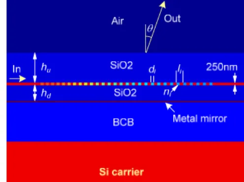
The proposed grating coupler is schematically depicted in Fig. 1. Its design is based on flip-chip bonding of a silica-clad fully etched silicon PhC grating coupler on a silicon carrier wafer. The thickness of the top silicon device layer is 250 nm. Along the grating, an artificial material is introduced for the scattering units with refractive index ni
changed, and length of scattering unit li is also changed. SiO2
is used as upper and lower cladding material with thicknesses of hu and hd, respectively. A metal mirror is introduced below
the lower cladding and is bonded to the silicon carrier wafer. The coupling angle is designed to be 15º. The mirror metal is titanium (Ti) with thickness of 100 nm. In the design, the artificial material slot width is fixed to be 345 nm, and the scattering strength is tuned by changing ni and li. The
distributions of ni and li of the grating coupler are designed as
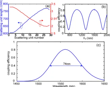
shown in Fig. 2(a). The detailed design method can be found in [7]. The lower cladding thickness hd plays an important
role on the coupling efficiency. Fig. 2(b) shows the coupling efficiency of the transverse electric (TE) mode as a function of hd calculated by two-dimensional (2D) eigenmode
expansion method (EME) with hu set to 1 µm. One can find
that the coupling efficiency depends periodically on hd, and
reaches a maximum at hd=1600 nm. With hd=1600 nm, the
coupling efficiency is further calculated as a function of wavelength, as shown in Fig. 2(c). A peak coupling efficiency of 81% (corresponding to 0.91 dB coupling loss) is predicted at 1560 nm with a 3 dB bandwidth of 74 nm. The
Fig. 1. Schematic structure of the proposed grating coupler.
Ultra-low coupling loss fully-etched apodized
grating coupler with bonded metal mirror
Yunhong Ding*, Christophe Peucheret*†, and Haiyan Ou* *Department of Photonics Engineering,
Technical University of Denmark, 2800 Kgs. Lyngby, Denmark Email: [email protected]
†University of Rennes 1 - ENSSAT,
Fig. 2. (a) Designed scattering unit length li and refractive index ni distributions of the grating coupler. (b) Simulated coupling efficiency as a function of lower cladding thickness. (c) Simulated coupling efficiency as a
function of wavelength with hd=1.6 µm and hu=1 µm.
artificial material slots are then replaced by a photonic crystal with triangular lattice [7], and the hole-diameters are calculated by the effective index approximation method.
III. DEVICE FABRICATION AND CHARACTERIZATION
The device was designed and fabricated on a commercial SOI sample with top silicon thickness of 250 nm and buried silicon dioxide (BOX) of 3 μm. Fig. 3 shows the fabrication process. A single step of standard SOI processing, including e-beam lithography and inductively coupled plasma (ICP) etching was first used to fabricate the grating coupler and silicon nano-waveguide simultaneously (see Fig. 3(a)). A 1600 nm thick layer of SiO2 was then deposited on top of the
grating coupler (see Fig. 3(b)), followed by deposition of 100 nm Ti (see Fig. 3(c)). Afterwards, about 2 μm benzocyclobutene (BCB) was spined on both the sample and silicon carrier wafer (see Fig. 3(d)). The sample was then flip-bonded on the silicon carrier wafer (see Fig. 3(e)) and thermally cured in a BCB oven. Finally the substrate of the chip was removed by ICP fast etching (see Fig. 3(f)). Fig. 4(a) and 4(b) show details of the fabricated device. In order to test the coupling loss, two identical grating couplers were fabricated with a 700 µm long single-mode straight waveguide introduced in between. The waveguide width was tapered from 12 µm for the grating couplers to 450 nm for the single mode straight waveguide with 500 µm tapering length. The propagation loss of the single mode silicon
Fig. 3. Fabrication process of the grating coupler with bonded mirror. (a) Grating coupler fabrication based on standard e-beam lithography and ICP etching. (b) SiO2 deposition. (c) Metallic mirror deposition. (d) BCB spinning
for both sample and carrier wafer. (e) Bonding. (f) Si substrate removal.
waveguide was measured to be 4 dB/cm. The fiber-to-fiber transmission was measured, and the coupling loss was calculated as half of the fiber-to-fiber transmission minus the propagation loss in the straight wave- guide. An ultra-low coupling loss of 1.25 dB (corresponding to 74% coupling efficiency) was obtained at 1560 nm with a 3 dB coupling bandwidth of 69 nm, as shown in Fig. 4(c), in good agreement with the numerical predictions. In order to test the fabrication tolerance, the size of the holes was increased by
dhole 8 nm, resulting in a peak coupling wavelength shift of 20 nm without peak coupling efficiency degradation. To the best of our knowledge, this is the lowest coupling loss ever reported for fully etched grating couplers.
Fig. 4. (a) Scanning electron microscopy (SEM) image and (b) optical microscopy image of the fabricated grating coupler. (c) Measured coupling
loss of the fabricated coupler with and without hole size change.
IV. CONCLUSION
We have designed and demonstrated a fully etched apodized grating coupler using PhCs with bonded mirror. A record low coupling loss of only 1.25 dB was measured with 3 dB coupling bandwidth of 69 nm.
V. ACKNOWLEDGEMENT
This work is supported by the Danish Council for Independent Research (project 1337-00152).
REFERENCES
[1] T. Tamir and S. T. Peng, “Analysis and design of grating couplers,” Appl. Phys., vol. 14, pp. 235–254, 1977.
[2] D. Taillaert, et al. , “An out-of-plane grating coupler for efficient butt-coupling between compact planar waveguides and single-mode fibers,” IEEE J. Quantum Electron., vol. 38, pp. 949–955, 2002. [3] R. Halir, et al., “Continuously apodized fiber-to-chip-surface coupler
with refractive index engineered subwavelength structure,” Opt. Lett., vol. 35, pp. 3243–3245, 2010.
[4] L. Liu, et al., “High-efficiency, large-bandwidth silicon-on-insulator grating coupler based on a fully-etched photonic crystal structure,” Appl. Phys. Lett., vol. 96, pp. 051126, 2010.
[5] F. V. Laere, et al., “Compact grating couplers between optical fibers and silicon-on-insulator photonic wire waveguides with 69% coupling efficiency,” in OFC’2006, U.S., paper PDP15.
[6] W. S. Zaoui, et al., “Bridging the gap between optical fibers and silicon photonic integrated circuits,” Opt. Express, vol. 22, pp. 1277–1286 (2014).
[7] Y. Ding, et al., “Ultra-high-efficiency apodized grating coupler using fully etched photonic crystals,” Opt. Lett., vol. 38, pp. 2732–2734, 2013.