HAL Id: pastel-00917826
https://pastel.archives-ouvertes.fr/pastel-00917826
Submitted on 12 Dec 2013
HAL is a multi-disciplinary open access archive for the deposit and dissemination of sci-entific research documents, whether they are pub-lished or not. The documents may come from teaching and research institutions in France or abroad, or from public or private research centers.
L’archive ouverte pluridisciplinaire HAL, est destinée au dépôt et à la diffusion de documents scientifiques de niveau recherche, publiés ou non, émanant des établissements d’enseignement et de recherche français ou étrangers, des laboratoires publics ou privés.
grown SiNWs and organic semiconducting polymers
Taewoo Jeon
To cite this version:
Taewoo Jeon. Nanostructured hybrid solar cells based on PECVD grown SiNWs and organic semi-conducting polymers. Electronics. Ecole Polytechnique X, 2013. English. �pastel-00917826�
E C O L E P O L Y T E C H N I Q U E
Doctoral Thesis in Physics and Materials Science
Nanostructured hybrid solar cells based on PECVD grown
SiNWs and organic semiconducting polymers
T
AEWOOJEON
THÈSE
présentée en vue d’obtenir le grande deDocteur de l’ Ècole Polytechnique
Spécialité : Physique et Science de Materiaux parT
AEWOOJEON
Nanostructured hybrid solar cells based on
PECVD grown SiNWs and organic semiconducting polymers
Thése soutenue le 25 Novembre 2013 devnat le jury composé de :Prof. Bernard Ratier Rapporteur
Prof. Joaquim Puigdollers Rapporteur
Dr. Daniel Lincot Examinateur
Dr. Thomas Heiser Examinateur
Prof. Yvan Bonnassieux Directeur de Thèse
A
CKNOWLEDGEMENTSI could complete my thesis, which is a subject quite challenging and multidisciplinary, by great helps of all colleagues at LPICM. First of all, I sincerely thanks to my thesis advisor, Prof. Yvan Bonnassieux, for his wholehearted support and a guidance that make me encourage and motivate. I express my gratitude to Dr. Bernard Geffroy, who was co‐advisor of the thesis, for his kind discussion on the subjects with helpful comments. Also, I thank to Prof. Pere Roca I Cabarrocas for his passions and curiosity that let me very motivate.
I can’t forget ORGATECH members who give me a technical support, discussion and a joyful laboratory life during my stay. I would like to thank to Denis Tondelier, Abderrahim Yassar, Gaël Zucchi, Jean‐Charles Vanel, François Moreau, Chang‐Hyun Kim, Hassina Derbal‐Habak, Subimal Majee, Xiaoguang Huang, and Jinwoo Choi. I am grateful to members of SiNWs team; Linwei Yu, Benedict O’Donnell, Soumyadeep Misra and Alienor Togonal. They helped me a lot for the SiNWs growth. The discussion with them gave ma insights on the SiNWs. And I thank to also Serge Palacin, Bruno Jousselme, and Pascale Jegou, who are the members of CEA for their helps for scientific discussion. I am especially grateful to Dmitri Daineka, Mark Chaigneau, Jinyoun Cho, Mun‐Ho Song, Antoine Salmon, Romain Cariou, Igor sobkowicz, Ka‐Hyun Kim, Chang‐Seok Lee, Ki‐Hwan Kim, Poncho Torres Rios, Junzhuan Wang, Youn‐ Ho Heo, Joonwon LIM, Jongwoo Jin, Youngbin Jeong, Myungjin Lim, Tae‐Ha Hwang, Ki‐Hwan Seok, Hojoong Kwon, Sungyeop Jeong, Heejae Lee, Jongyoon Park, Gijun Seo, and Haena Won.
I express my love and gratitude to my wife, Eunjung PARK, and my son, Yesung JEON, and also to my family in Korea for their love and faith for me.
i
C
ONTENTSAcknowledgements Contents ··· i List of Figures ··· v List of Tables ··· xi List of Acronyms ··· xiii CHAPTER 1 ‐ BACKGROUND KNOWLEDGE ··· 1 1.1 INTRODUCTION ··· 2 1.2 SILICON MATERIALS ··· 2 1.2.1 SILICON NANOWIRES ··· 2 1.2.2 HYDROGENATED AMORPHOUS SILICON ··· 6 1.3 ORGANIC SEMICONDUCTOR ··· 7 1.3.1 Π‐CONJUGATED SYSTEM ··· 7 1.3.2 P3HT AND PCBM ··· 9 1.3.3 PEDOT:PSS ··· 11 1.4 CHARACTERIZATION OF MATERIALS AND SOLAR CELLS··· 12 1.4.1 SCANNING ELECTRON MICROSCOPE ··· 12 1.4.2 RAMAN SPECTROSCOPY ··· 13 1.4.3 X‐RAY PHOTOEMISSION SPECTROSCOPY ··· 15 1.4.4 UV‐VIS SPECTROSCOPY ··· 15 1.4.5 CURRENT‐VOLTAGE CHARACTERISTICS OF SOLAR CELLS ··· 17 1.5 HYBRID SOLAR CELLS BASED ON SILICON AND ORGANIC MATERIALS ··· 22 1.6 APPROACHES OF THESIS ··· 27 Reference ··· 28 CHAPTER 2 ‐ PECVD GROWTH OF SINWS AND NANO‐MORPHOLOGY ··· 33 2.1 INTRODUCTION ··· 34 2.2 PLASFIL SYSTEM (PECVD) ··· 35 2.3 VLS GROWTH OF SINWS AND CATALYST CHOICE ··· 37 2.4 SN‐CATALYZED SINWS ··· 41 2.4.1 GROWTH TIME DEPENDENCE ··· 43 2.4.2 DENSITY CONTROL BY H2 PLASMA ··· 46 2.5 BI‐CATALYZED SINWS ··· 49 2.5.1 N‐TYPE CHARACTERISTIC OF BI‐CATALYZED SINWS ··· 50
ii 2.5.2 TEMPERATURE DEPENDENCE ··· 51 2.5.3 RF POWER DEPENDENCE ··· 54 2.5.4 GAS FLOW RATIO DEPENDENCE ··· 56 2.6 CONCLUSION: PROPER USE OF EACH SINWS ··· 60 2.6.1 SN‐CATALYZED SINWS ··· 60 2.6.2 BI‐CATALYZED SINWS ··· 61 Reference ··· 63 CHAPTER 3 ‐ NANO‐STRUCTURED HYBRID SOLAR CELLS··· 67 3.1 INTRODUCTION ··· 68 3.2 DEVICE DESIGN, FABRICATION AND WORKING PRINCIPLE ··· 70 3.3 PHOTOVOLTAIC EFFECT ESTABLISHMENT BY PEDOT:PSS··· 74 3.4 MORPHOLOGY OF SINWS & PHOTOVOLTAIC EFFECTS ··· 86 3.5 CONCLUSION: REQUIREMENTS FOR PHOTOVOLTAIC ACTION ··· 93 Reference ··· 95 CHAPTER 4 ‐ OPTIMIZATION OF SINWS FOR EFFICIENT LIGHT TRAPPING ··· 99 4.1 INTRODUCTION ··· 100 4.2 ACID TREATMENTS FOR RESIDUAL CATALYST REMOVAL ··· 102
4.2.1 HCL TREATMENT OF SINWS AND ITS EFFECT ON SINWS ARRAY ··· 102
4.2.2 EFFECTS OF ACID TREATMENTS ON HYBRID SOLAR CELL PERFORMANCE ··· 112
4.3 A‐SI:H ETCHING BY HYDROGEN PLASMA ··· 123
4.3.3 SELECTIVE ETCHING OF A‐SI:H FROM SINWS ARRAY ··· 123
4.3.4 ENHANCED SOLAR CELL PERFORMANCE BY A‐SI:H ETCHING ··· 130 4.4 CONCLUSION: BENEFITS FROM SN‐CATALYZED SINWS ··· 137 Reference ··· 141 CHAPTER 5 ‐ HYBRID HETEROJUNCTION BASED SOLAR CELL ··· 143 5.1 INTRODUCTION ··· 144 5.2 HYBRID INTERFACE: P3HT AND SILICON MATERIALS ··· 144 5.3 REALIZATION OF HYBRID SOLAR CELLS ··· 148
iii 5.4 DEVICE PERFORMANCES ··· 150 5.4.1 DARK CURRENT‐VOLTAGE CHARACTERISTIC ··· 150 5.4.2 SOLAR CELL PERFORMANCE ··· 153 5.5 CONCLUSION: CHALLENGES AND PERSPECTIVES ··· 161 Reference ··· 163 CONCLUSION ··· 167 APPENDIX ··· 169 A.1 TCO DEPENDENCE OF HYBRID SOLAR CELL PERFORMANCE ··· 170 A.2 SINWS GROWTH CONDITIONS ··· 171
A.2.1 SN‐CATALYZED SINWS: GROWTH TIME DEPENDENCE (SECTION 2.4.1) ··· 171
A.2.2 SN‐CATALYZED SINWS: H2 DEPENDENCE (SECTION 2.4.2) ··· 171
A.2.3 BI‐CATALYZED SINWS: TEMPERATURE DEPENDENCE (SECTION 2.5.2) ··· 172
A.2.4 BI‐CATALYZED SINWS: RF POWER DEPENDENCE (SECTION 2.5.3) ··· 172
A.2.5 BI‐CATALYZED SINWS: GAS FLOW RATIO DEPENDENCE (SECTION 2.5.4) ··· 172
A.3 ORGANIC THIN‐FILM FORMATION ··· 173
iv
v
L
IST OFF
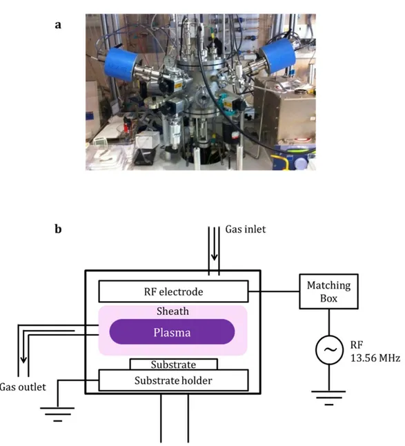
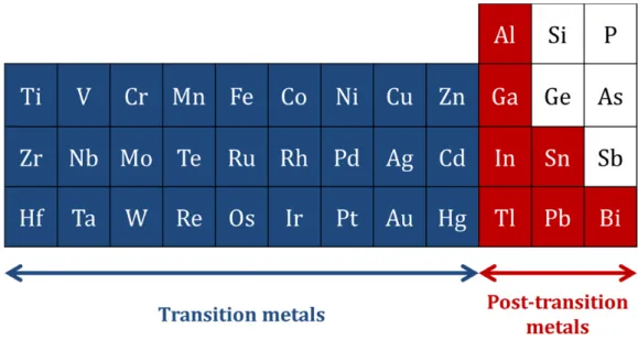
IGURESFigure 1.1 – Band diagram of crystalline silicon with characterized energy level based on vacuum levels. ··· 3 Figure 1.2 – Absorptance of silicon thin film and silicon nanowires as a function of photon energy of incident light. ··· 4 Figure 1.3 – Benefits of silicon nanowire fabricated by (a) etching of crystalline silicon and (b) plasma‐ enhanced chemical vapor deposition. ··· 5 Figure 1.4 – Density of states of hydrogenated amorphous silicon. Exponential band tail states and deep states are illustrated. ··· 6 Figure 1.5 – Graphical description of π‐conjugated system: (a)the example of Benzene (b) bonding between 2 π‐orbitals. According to the wave function overlap, bonding and anti‐bonding states are generated. ··· 7 Figure 1.6 – Energy band formation in organic materials with increased number of atoms. π and π* band is described with HOMO and LUMO levels. ··· 8 Figure 1.7 – Molecular structure of (a) P3HT and (b) PCBM ··· 9 Figure 1.8 – Molecular structure of PEDOT:PSS ··· 11 Figure 1.9 – Examples of SEM images: (a) Tin‐catalyzed SiNWs (b) Bismuth‐catalyzed SiNWs by PECVD ··· 13 Figure 1.10 – Raman spectrum of Sn‐catalyzed SiNWs. Crystal silicon peak is observed at 518 cm‐1 with amorphous silicon peak (broad) at 480 cm‐1. ··· 14 Figure 1.11 – Absorbance measured by UV‐Vis spectroscopy. SiNWs, P3HT:PCBM and SiNWs with P3HT:PCBM are measured based on the same base line ··· 16 Figure 1.12 – Air mass; solar spectral irradiance as a function of wavelength Inset shows incident angle of sunlight relative to zenith (normal to the earth’s surface). ··· 18 Figure 1.13 – A typical solar cell J‐V curve with solar cell parameters. ··· 19 Figure 1.14 – Equivalent circuit model of solar cell consisted of constant current source, diode, series and shunt resistance. ··· 20 Figure 1.15 – The example of type 1 hybrid solar cell based on n‐type silicon nanocone and PEDOTPSS. (a) solar cell structure and (b) solar cell performance ··· 23 Figure 1.16 – The example of type 2 hybrid solar cells based on P3HT and silicon nanocrystals. (a) solar cell structure (b) absorbance and (c) solar cell performance ··· 24 Figure 1.17 ‐ The example of type 3 hybrid solar cell based on n‐type silicon wafer and P3HT. (a) solar cell structure and (b) solar cell performance ··· 25 Figure 2.1 – SEM images of SiNWs fabricated by top‐down (TD) approaches and bottom‐up (BU) approaches. By (a) reactive ion etching (TD) (b) metal‐catalyzed electro‐less etching (TD) (c) chemical vapor deposition (BU) (d) plasma‐enhanced chemical vapor deposition (BU) ··· 34 Figure 2.2 – PECVD system; (a) The photo of PLASFIL system used in this study, (b) Schematic diagram of PLASFIL ··· 36 Figure 2.3 – Schematic diagrams of vapor‐liquid‐solid process. (a) Catalyst metal film deposition (b) catalyst droplet formation (c) dissociation of precursor gas (in this case silane) (d) diffusion of silicon atoms into catalyst droplets (e) continuous integration and diffusion of silicon atoms in catalyst droplets (f) crystalline phase of silicon is precipitated at the interface after the silicon concentration reaches saturation. ··· 38 Figure 2.4 – Periodic table of transition metals and post‐transition metals as potential catalyst metals for VLS process. ··· 39
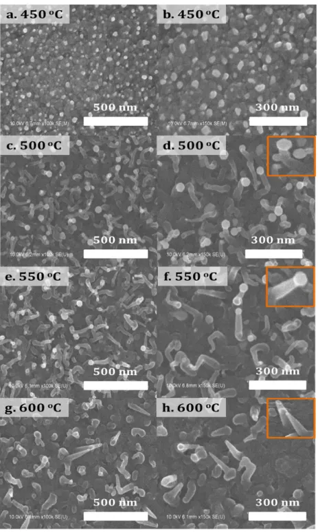
vi Figure 2.5 – Impurities energy level of catalyst metals as a function of eutectic point with silicon. Red triangles and blue squares correspond to post‐transition and transition metals respectively. ··· 40 Figure 2.6 – Sn‐catalyzed SiNWs growth procedures by PECVD. (a) Hydrogen plasma of thin tin deposited ITO/glass substrate (b) Silane plasma with tri‐methyl boron for SiNWs growth (c) VLS growth process and (d) Sn‐catalyzed SiNWs array. ··· 42 Figure 2.7 – SEM images of Sn‐catalyzed SiNWs with the growth time (a) 5 min (b) 5 min, cross‐sectional view (c) 10 min and (d) 15 min ··· 43 Figure 2.8 – Length and diameter of SiNWs as a function of growth time. (Black symbol and line for length, Red symbol and line for diameter) ··· 44 Figure 2.9 – Absorbance of SiNWs for SiNWs arrays of different growth time ··· 45 Figure 2.10 – SEM images of Sn‐catalyzed SiNWs depending on hydrogen plasma duration during catalyst droplets formation. (a) 2 min (b) 4 min (c) 6 min and (d) 8 min. ··· 46 Figure 2.11 – Dimensional characteristics of SiNWs depending on hydrogen plasma duration during catalyst formation. (a) Density (b) Diameter and (c) Length of Sn‐catalyzed SiNWs. ··· 47 Figure 2.12 – Schematic diagram of catalyst generation from thin Sn film and also from ITO. (a) Thin Sn metal deposited on ITO/glass, (b) Hydrogen plasma at 350 oC at the beginning (c) Long time hydrogen plasma at 350 oC. In catalyst starts to generate. (d) Presence of Sn and In catalyst droplets ··· 48 Figure 2.13 – SEM images of Bi‐catalyze SiNWs depending on growth temperature. Growth temperatures are (a,b) 450 oC (c,d) 500 oC (e,f) 550 oC and (g,h) 600 oC. ··· 52
Figure 2.14 – Density and residual catalyst diameters as a function of growth temperature. (Black symbol and line for density, Red symbol and line for residual catalyst diameter) ··· 53
Figure 2.15 – SEM images of Bi‐catalyze SiNWs depending RF power (a,b) 20 W (c,d) 40 W and (e,f) 60 W ··· 54
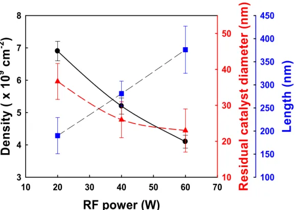
Figure 2.16 – Density, residual catalyst diameters and length as a function of RF power. (Black symbol and line for density, Red symbol and line for residual catalyst diameter, Blue symbol and line for SiNWs’ length)··· 55
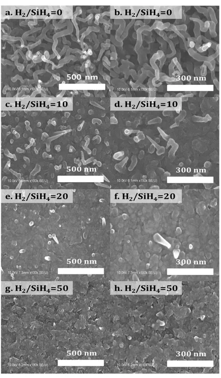
Figure 2.17 – SEM images of Bi‐catalyze SiNWs depending gas flow ratio (H2/SiH4). (a,b) 0 (c,d) 10 (e,f) 20 and (g,h) 50 ··· 57
Figure 2.18 – Density and length as a function H2/SiH4 ratio. (Black symbol and line for density, Red symbol and line for SiNWs’ length) ··· 58 Figure 2.19 – Etching of residual bismuth catalyst on tip of SiNWs by hydrogen plasma at 600 oC. ··· 59 Figure 2.20 – (a) SEM image of Sn‐catalyzed SiNW and (b) spacing between SiNWs: Mean spacing is 180 nm. ··· 60 Figure 2.21 – SEM image: Nano‐morphology variation of Bi‐catalyzed SiNWs ··· 61 Figure 2.22 – (a) SEM image of Bi‐catalyzed SiNW and (b) spacing between SiNWs: Mean spacing is 20 nm. ··· 62 Figure 3.1 – Representatives of hybrid solar cells device structures (a) bi‐layer type (b) blend type (c) nano‐ structure type ··· 68 Figure 3.2 – Description of spin‐coating method; (a) dispensation of prepared solution on substrate (b) spin‐ up stage (c) spin‐off and film formation and (d) the photo of spin‐coating process photo ··· 70 Figure 3.3 – Film thickness of (a) P3HT dissolved in 1,2‐Dichlorobenzene according to the solution concentration from 2 mg/mL to 30 mg/mL and (b) PEDOT:PSS according to the rotation speed from 3000 rpm to 4000 rpm. ··· 71 Figure 3.4 – Nano‐structured hybrid solar cell fabrication process (a) as grown Sn‐catalyzed SiNWs, (b) deposition of PEDOT:PSS buffer layer by spin coating, (c) deposition of P3HT:PCBM layer on PEDOT:PSS and (d) final device with LiF/Al top electrode. ··· 72
vii Figure 3.5 – Band diagram explaining general working principle of organic solar cells which is quite similar with the hybrid solar cell in this study. ··· 73 Figure 3.6 – Absorbance of P3HT:PCBM layer on glass (dashed line) and SiNWs (solid line) ··· 75 Figure 3.7 – Current density‐voltage characteristics of hybrid solar cells under dark (black, left y‐axis in semi‐ log scale) and AM 1.5 (red, right y‐axis in linear scale). The inset figure describes device structure (Glass/ITO/SiNWs/P3HT:PCBM/LiF/Al) ··· 76 Figure 3.8 – Hybrid solar cells performances according to the PEDOT:PSS existence and thickness (a) under AM 1.5 illumination (b) dark··· 77 Figure 3.9 – SEM images of (a) as grown SiNWs and (b) SiNWs covered by PEDOT:PSS and Schematic diagram of (e) as grown SiNWs and (f) SiNWs covered by PEDOT:PSS ··· 79 Figure 3.10 – Schematic diagram of P3HT:PCBM layer on SiNWs (a) without, (b) with PEDOT:PSS and (c) energy band diagram of P3HT, PCBM, SiNWs ··· 81 Figure 3.11 – Transmittance of PEDOT:PSS layer on ITO with thickness variation ··· 83 Figure 3.12 – Experimental photo‐current density – effective voltage plots: Jph is extracted by the equation Jph=JL‐JD. ··· 84 Figure 3.13 – Model diagrams of hybrid solar cells according to length of SiNWs and organic active layer thickness. (a) length of SiNWs > thickness of P3HT:PCBM, (b) length of SiNWs ~ thickness of P3HT:PCBM and (c) length of SiNWs < thickness of P3HT:PCBM, ··· 87 Figure 3.14 – SEM images of hybrid solar cells case by case. (a) Case 1 on P3HT:PCBM. (b) Case 1 on P3HT:PCBM/LiF/Al (c) Case 2 on P3HT:PCBM and (d) Case 3 on P3HT:PCBM ··· 87 Figure 3.15 – Hybrid solar cell performance for three case of SINWs length and organic layer thickness relations. Measured under AM 1.5 condition. ··· 88 Figure 3.16 – Absorbance of P3HT:PCBM with different SiNWs density; SiNWs absorption is excluded. ··· 90 Figure 3.17 – Hybrid solar cell performance according to the density of SiNWs. Measured under AM 1.5 condition. ··· 91 Figure 3.18 – Series resistance dependence of (a) short‐circuit current and (b) power conversion efficiency. ··· 92 Figure 3.19 – Normalized external quantum efficiency of conventional organic bulk‐heterojunction solar cells and hybrid solar cells ··· 93 Figure 4.1 – Schematic diagrams of hybrid solar cells. (a) entire device structure of the hybrid solar cells based on PECVD grown SiNWs and P3HT:PCBM. This device can be divided into two sub‐devices (b) sub‐device 1 containing SiNWs and (c) sub‐device 2 without SiNWs. ··· 100 Figure 4.2 – SEM image of PECVD grown Sn‐catalyzed SiNWs on ITO/glass substrate; 1) Thickness of Sn: 2 nm 2) Catalyst droplets formation (H2 plasma): 350 ℃, 100 sccm of H2, 360 mTorr, 5 W, 2 min 3) SiNWs growth: 600 ℃, 10 sccm of SiH4, 1.5 sccm of TMB, 100 sccm of H2, 1 Torr, 2 W, 3 min ··· 102 Figure 4.3 – Solar cell performance of organic bulk‐heterojunction solar cells based on P3HT:PCBM with and without 1 nm of Tin on ITO under A.M 1.5 ··· 103 Figure 4.4 – Dipping of SiNWs into 5 % HCl to remove residual Sn; the dipping time is optimized by 20 min with consideration of SiNWs’ damage ··· 105 Figure 4.5 – Sheet resistance of ITO with HCl dipping time ··· 106 Figure 4.6 – SEM images of Sn‐catalyzed SiNWs array after dipping into HCl with different time. All SiNWs array was grown with identical condition; 1) Thickness of Sn: 2 nm 2) Catalyst droplets formation (H2
viii plasma): 350 ℃, 100 sccm of H2, 360 mTorr, 5 W, 2 min 3) SiNWs growth: 600 ℃, 10 sccm of SiH4, 1.5 sccm of TMB, 100 sccm of H2, 1 Torr, 2 W, 3 min ··· 107 Figure 4.7 – Results of X‐ray photoelectron spectroscopy of SiNWs array with different HCl dipping time for detecting residual catalyst (here, Sn). The graph describes normalized counts of Sn metal and oxide part as a function of binding energy. Sn metal and oxide are detected at 484.9 and 487.2 eV respectively. The inset table summarizes ratio of Sn metal and oxide compared with silicon according to the HCl dipping time. ··· 108 Figure 4.8 – Schematic of distributed catalyst on as grown SiNWs array (cross‐sectional view). (1) residual catalyst after growth (2) ultra‐thin diffused catalyst on SiNWs’ surface (3) Diffused SiNWs during the growth in SiNWs and (4) catalyst droplets covered by a‐Si:H before initiating SiNWs growth. ··· 109 Figure 4.9 – Transmittances of (a) ITO/glass substrate and (b) SiNWs/ITO/glass substrate as a function of wavelength with various HCl dipping time. ··· 110 Figure 4.10 – Current density – voltage characteristics under dark with various HCl treatments. ··· 113 Figure 4.11 – Solar cell performance of hybrid solar cells under illumination intensity (a) 13 mW/cm2 and (b) 100 mW/cm2 with various HCl dipping time. ··· 114
Figure 4.12 – Open‐circuit voltage (Voc) change as a function of HCl dipping time; Voc is measured under AM
1.5 conditions. ··· 117 Figure 4.13 – Light intensity dependence of open‐circuit voltage with various HCl dipping time. Linear fits for the data are drawn in solid line. While dashed line is drawn as an eye guide line for the slope of kT/q. ··· 120 Figure 4.14 – Dark current density – voltage characteristics with and without HF treatment. ··· 121 Figure 4.15 – Solar cell performance with and without HF treatment measured under AM 1.5 condition ··· 122 Figure 4.16 – Solar cell performance with and without a‐Si:H layer (10 nm) on ITO/glass substrate. Measured under AM 1.5 condition. ··· 125 Figure 4.17 –Raman spectroscopy of Sn‐catalyzed SiNWs array measured by 621 nm wavelength of red laser with 0.15 mW light intensity. (a) Mapping images over 7 x 7 μm2, (b) Raman shift of SiNWs dominant region and (c) Raman shift of a‐Si:H dominant region; SiNWs have diameter, length and density of 20 nm, 240 nm and 4.0 x 10⁹ SiNWs/cm2 ··· 126 Figure 4.18 – Schematic diagram of amorphous silicon etching process by hydrogen plasma; Big dark circle, small yellow and red circles represent silicon atoms, hydrogen atoms bonded during SiNWs growth for hydrogenation and hydrogen atoms supplied by hydrogen plasma. Grey solid lines mean covalent bond between atoms. Dark solid line depicts etching process of a‐Si:H and dark dashed line indicates less sensitivity
of SiNWs. H2 plasma is performed at 100 oC with flow rate, pressure and RF power of 200 sccm, 1 Torr and 20
W respectively. ··· 127 Figure 4.19 – Absorbance of SiNWs/ITO/Glass substrates according to the hydrogen plasma time ··· 129 Figure 4.20 – Dimensional properties of SiNWs array according to the hydrogen plasma duration. (a) Diameter of SiNWs, (b) Length of SiNWs, (c) density of SiNWs, and SEM images (d) 0s, (e) 90 s (f) 180 s of duration of hydrogen plasma. The white scale bars indicate 500 nm ··· 130 Figure 4.21 – Solar cells performance according to the a‐Si:H etching duration by hydrogen plasma ··· 132 Figure 4.22 – Absorbance of P3HT:PCBM film on SiNWs treated by hydrogen plasma. ··· 133 Figure 4.23 – Schematic diagram of holes transport from P3HT:PCBM layer to a‐Si:H layer. [a] electron transfer from P3HT to PCBM [b] hole transport through P3HT to PEDOT:PSS [c] Injection of holes from PEDOT:PSS to a‐Si:H (energy barrier, ф, is 0.5 eV) and [d] hole transport through band‐gap states ··· 134 Figure 4.24 – Experimental photo‐current as a function of effective voltage (V0‐V) according to the H2 plasma duration. ··· 135
ix Figure 4.25 – Solar cells performance according to the optimization method which are measured under AM 1.5 condition. ··· 138 Figure 4.26 – Normalized external quantum efficiency (EQE) of solar cells; comparison of organic bulk‐ heterojunction solar cells (BHJ SC) and hybrid solar cell (HSC) with different treatment conditions. Organic active layer is composed of P3HT and PCBM. The thickness of active layer is same for BHJ SC and HSC. ··· 139 Figure 5.1 – Energy band diagrams of P3HT, crystalline silicon (c‐Si) and hydrogenated amorphous silicon (a‐ Si:H) ··· 145 Figure 5.2 – Solar cell based on c‐Si/P3HT junction. (a) Solar cell structure: P3HT is spin‐coated on n‐Si wafer, and then semi‐transparent palladium is evaporated. (b) Solar cell performance with various thickness of P3HT. (Reprinted from Ref.[3]) ··· 146 Figure 5.3 – Solar cell based on a‐Si:H/P3HT junction. (a) Solar cell structure: n‐type a‐Si:H are deposited by conventional PECVD with 20 nm thick. P3HT is spin‐coated on a‐Si:H layer and then silver (Ag) electrode is deposited by thermal evaporation. (b) Solar cell 0performance. ··· 147 Figure 5.4 – Characteristics of Bi‐catalyzed SiNWs. (a) SEM image: dense SiNWs are chosen for exciton dissociation and (b) Raman spectroscopy: crystalline silicon peak is observed with broad amorphous silicon peak. ··· 148 Figure 5.5 – Hybrid solar cell structures based on Bi‐catalyzed SiNWs on aluminum doped zinc oxide and P3HT with grid silver electrode. ··· 149 Figure 5.6 – Dark current density – voltage characteristics of the hybrid solar cell based on Bi‐catalyzed SiNWs/P3HT interface. Diode parameters are summarized in the graph. ··· 151 Figure 5.7 – Dark current density – voltage characteristics of the hybrid solar cell based on Bi‐catalyzed SiNWs/P3HT interface. Diode parameters are summarized in the graph. ··· 152 Figure 5.8 – Solar cell performance of the hybrid solar cell based on Bi‐catalyzed SiNWs/P3HT interface. Solar cell parameters are summarized in the graph. Average length of Bi‐catalyzed SiNWs and thickness of solar cell are 130 and 150 nm respectively. ··· 153 Figure 5.9 – Band diagram of SiNWs P3HT to explain photo‐generated carrier generation. 1) Exciton generation by absorption of incident light. 2) Diffusion of exciton toward interface of SiNWs/P3HT. 3) Exciton dissociation (electron transfer from LUMO of P3HT to conduction band of SiNWs) 4) electron recombination 5) Transport of photo‐generated carriers ··· 154 Figure 5.10 – Solar cell performance of the hybrid solar cell based on Bi‐catalyzed SiNWs/P3HT interface; dependence of PCBM contents (%) in P3HT solution ··· 155
Figure 5.11 – (a) Jsc and Voc of hybrid solar cells as a function of PCBM content (%) (b) Experimental photo‐
current extracted from the equation of JL‐JD=Jph as a function of effective voltage, V0‐V. ··· 156 Figure 5.12 – Solar cell performance of planar solar cell without SiNWs. Solar cell parameters are summarized in the graph. ··· 159 Figure 5.13 – Summary of solar cell performance of hybrid heterojunction based on SiNWs/P3HT, SiNW/P3HT:PCBM and organic inverted solar cells based on P3HT:PCBM. ··· 160
x
xi
L
IST OFT
ABLESTable 1.1 – Summary of types of hybrid solar cells based on light absorbing materials. ··· 22 Table 3.1 – Summary of solar cell parameters with various PEDOT:PSS thickness ··· 78 Table 3.2 – Summary of hybrid solar cell parameters case by case ··· 88 Table 3.3 – Summary of hybrid solar cell parameters with various SiNWs density··· 91 Table 4.1 – Summary of solar cell parameters with substrates ··· 103 Table 4.2 – Series and shunt resistance of hybrid solar cells under dark with various HCl dipping time. ··· 113 Table 4.3 ‐ Hybrid solar cells parameters with various HCl dipping time. ··· 115 Table 4.4 – Diode parameters of hybrid solar cells: dependence of HF treatment ··· 120 Table 4.5 – Solar cell parameters of hybrid solar cells: dependence of HF treatment ··· 121 Table 4.6 – Solar cell parameters of hybrid solar cells: dependence of a‐Si:H layer existence. ··· 125 Table 4.7 – Solar cells parameters of hybrid solar cells: dependence of a‐Si:H layer existence ··· 131
xii
xiii
L
IST OFA
CRONYMSAcronym a‐Si:H Hydrogenated amorphous silicon AZO Aluminum‐doped zinc oxide c‐Si Crystalline silicon CVD Chemical vapor deposition Ebinding Binding energy (eV) Egap Band‐gap (eV) EQE External quantum efficiencies FF Fill factor (%) HOMO Highest Occupied Molecular Orbital ITO Indium tin oxide J0 Reverse saturation current (mA/cm2) JD‐V Dark current density ‐ voltage characteristic
JL‐V Illumination current density ‐ voltage characteristic
Jph Photo‐current density (mA/cm2) Jsc Short‐circuit current (mA/cm2) LUMO Lowest Unoccupied Molecular Orbital n Diode ideality factor P3HT Poly(3‐hexylthiophene) PCBM Phenyl‐C61‐butyric acid methyl ester PECVD Plasma enhanced chemical vapor deposition PEDOT:PSS Poly(3,4‐ethylenedioxythiophene) poly(styrenesulfonate) Plight Incident light intensity (mW/cm2) Pmax Maximum power (mW/cm2) rpm Revolutions per minute Rs Series resistance (Ω·cm2) Rsh Shunt resistance (Ω·cm2) sccm Standard cubic centimeters per minute SEM Scanning electron microscope SiNWs Silicon nanowires T Absolute temperature (K) V0 Defined as voltage where JL=0 (V) VLS Vapor‐liquid‐solid Voc Open‐circuit voltage (V) XPS X‐ray photoemission spectroscopy (eV) η Power conversion efficiency of solar cell (%) ф Work function (eV)
xiv
1
Chapter 1
B
ACKGROUND KNOWLEDGE1.1 INTRODUCTION ··· 2 1.2 SILICON MATERIALS··· 2 1.2.1 SILICON NANOWIRES ··· 2 1.2.2 HYDROGENATED AMORPHOUS SILICON ··· 6 1.3 ORGANIC SEMICONDUCTOR ··· 7 1.3.1 Π‐CONJUGATED SYSTEM ··· 7 1.3.2 P3HT AND PCBM ··· 9 1.3.3 PEDOT:PSS ··· 11 1.4 CHARACTERIZATION OF MATERIALS AND SOLAR CELLS ··· 12 1.4.1 SCANNING ELECTRON MICROSCOPE ··· 12 1.4.2 RAMAN SPECTROSCOPY ··· 13 1.4.3 X‐RAY PHOTOEMISSION SPECTROSCOPY ··· 15 1.4.4 UV‐VIS SPECTROSCOPY ··· 15 1.4.5 CURRENT‐VOLTAGE CHARACTERISTICS OF SOLAR CELLS ··· 17 1.5 HYBRID SOLAR CELLS BASED ON SILICON AND ORGANIC MATERIALS ··· 22 1.6 APPROACHES OF THESIS ··· 27 REFERENCE ··· 28
2
1.1 Introduction
Here, backgrounds needed to figure out this thesis are briefly introduced. For materials, silicon and organic materials used such as amorphous silicon, silicon nanowires (crystalline silicon), poly‐ 3(hexylthiophene), phenyl‐C61‐butyric methyl ester and poly(3,4‐ ethylenedioxythiophene) poly(styrenesulfonate), are presented. Methods to characterize these materials, for instance, scanning electron microscope, Raman spectroscopy and UV‐visible spectroscopy will be briefly discussed. Furthermore, the basic of solar cells, solar cell parameters and measurement methods are covered. Various types of hybrid solar cells developed during the last decade will be explained according to the working principle for better understanding of hybrid solar cells. Finally, our approaches to organize silicon and organic materials for hybrid solar cell development will be discussed.
1.2 Silicon materials
1.2.1 Silicon nanowires
Silicon is the most popular semiconductor material for solid‐state electronics. For examples, first silicon solar cell based on p‐n junction was presented in 1954 by Chapin et al [1]. Despite of the rapid development of novel materials such as organic materials, carbon nanotube and graphene, the silicon based electronics are supported by the abundance of material and the technical maturity. In recent year, numerous nano‐structures of silicon are drawing strong attentions as efficient energy conversion materials due to their unique characteristics compared to the bulk silicon wafer, for examples nanoparticles [2], nanowires [3‐12], nanorods [13, 14] etc. The physical properties of the nanostructured silicon are adjustable by changing their dimensional characteristics and nano‐morphologies. Among them, silicon nanowires (SiNWs) are one of most interesting configuration because the geometry of nanowires provides the smallest dimension for light trapping, photo‐carrier generation, separation and transport [15].
Chapter 1 – Background knowledge
3
Figure 1.1 – Band diagram of crystalline silicon with characterized energy level based on vacuum levels.
SiNWs are rod‐like crystalline silicon with diameter less than 100 nm. SiNWs stands on the basis of silicon whisker reported in 1957 by Treuting and Arnold where they presented <111> direction of silicon whiskers [16]. And Wagner and Ellis reported vapor‐liquid‐solid mechanism of SiNWs growth, which is still predominant mechanism of SiNWs growth, in 1964 [17]. A boom in research of SiNWs was started from 1998 in earnest with over 100 publications. Next, the dramatic increase in the number of publication was made in 2003‐2007 with over 600 publications [18].
SiNWs fabrication methods can be largely classified into top‐down and bottom‐up approaches. Top‐down method is generally used to crystalline silicon wafer as a source material. Reactive ion etching and metal‐catalyzed electro‐less etching of silicon are employed for physical and chemical etching of bulk silicon wafer [19, 20]. These nanowires have same electrical characteristics with mother silicon wafer. However, the cost of silicon wafer is an obstacle for wide uses of this technique. Bottom‐up approaches are considered as an alternative for low cost SiNWs fabrication. Crystalline phase of SiNWs are synthesized by various methods. For examples, conventional chemical vapor deposition (CVD), plasma‐enhanced CVD, laser ablation, molecular beam epitaxy and silicon dioxide evaporation, etc. SiNWs
4
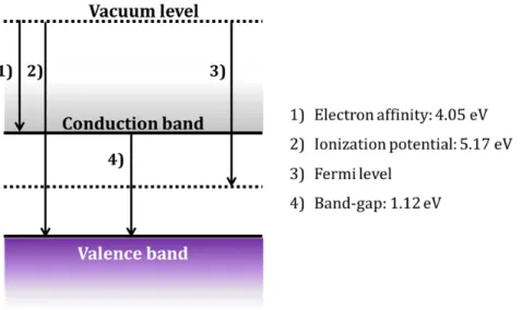
growth can be catalyzed by numerous catalyst metals. The electrical characteristics of SiNWs can be tuned by the choice of catalyst and process parameters like the type of doping gas, doping gas flow ratio, etc. Bottom‐up approaches commonly have higher degree of freedom in nano‐morphology control than that of top‐down approaches. As the SiNWs are crystalline, they have energetic band diagram of crystalline silicon illustrated in Figure 1.1. It describes electron affinity, ionization potential and band‐gap, having 4.05 eV, 5.17 eV and 1.12 eV at 300 K, respectively. Fermi level depends on the doping profile [21].
Figure 1.2 illustrates the optical characteristic of silicon film and SiNWs which was reported by Hu and Chen in 2007 [22]. SiNWs have quite different absorption curves compared to that of silicon thin film of same thickness. The nanowires have lower absorptance in lower photon energy while they show higher absorptance in higher photon energy regime compared to the thin‐film. For the SiNWs, low energy photons under 2 eV are just weakly absorbed in spite of higher energy than band‐gap of silicon. This is mainly attributed to the indirect band gap structure of crystalline silicon. The photon with higher energy than 2 eV, and it shows plateau region over 3 eV.
Figure 1.2 – Absorptance of silicon thin film and silicon nanowires as a function of photon energy of incident light [22].
Chapter 1 – Background knowledge
5
Figure 1.3 shows examples of SiNWs fabricated by top‐down and bottom‐up approaches. SEM image and optical characteristic such as reflectance and absorption are reprinted from the references [23, 24]. Figure 1.3 (a) shows SiNWs by the etching of silicon wafer. It results in a considerable decrease of reflectance. In other words, incident light is well trapped in silicon wafer thanks to the nanowire structure which increases solar cell performance. On the other hands, PECVD grown SiNWs with a hydrogenated amorphous silicon covering are shown in Figure 1.3 (b). The nanowires enhance light‐trapping in the hydrogenated amorphous silicon layer. The increase in absorption is observed with p‐i‐n structure. Optical characteristics of both types of SiNWs are modulated by changing their nano‐morphology and dimensional properties such as length, diameter, density, etc. Figure 1.3 – Benefits of silicon nanowire fabricated by (a) etching of crystalline silicon [24] and (b) plasma‐enhanced chemical vapor deposition [23].
6 1.2.2 Hydrogenated amorphous silicon Hydrogenated amorphous silicon (a‐Si:H) is a silicon material which has no periodic structure at all with hydrogen passivation of dangling bonds. It is still a fascinating light absorbing material for thin‐film solar cells based on p‐ i‐n or n‐i‐p structure due to its high absorption coefficient and easy fabrication on large and various substrates [23, 25, 26]. Since it has disordered structure, the optical and electrical characteristics quite differ from crystalline silicon. a‐Si:H has 1.75 eV of band‐gap and 1 μm thick of a‐ Si:H can absorb up to 90 % of incident light with the photon energy over band‐gap energy. The band structure of a‐Si:H is illustrated in Figure 1.4. The exponential band tails states on both conduction and valence bands and deep trap states are existed in the forbidden gap of a‐Si:H unlike crystalline silicon. This band structure is originated from no periodic bonding structure of a‐ Si:H and dangle bonds. If intrinsic a‐Si:H is doped by p‐ or n‐ type dopants, the defect density is more increased owing to the dopants. These mid‐gap states could be liable for the degradation of device performance. For examples, it promotes the recombination of photo‐generated carriers and increases resistive effects in solar cells.
Figure 1.4 – Density of state of hydrogenated amorphous silicon. Exponential band tail states and deep states are illustrated [27].
Chapter 1 – Background knowledge 7 It has to be taken into accounted that a‐Si:H is co‐deposited during the SiNWs growth by PECVD technique. a‐Si:H could be preferentially deposited on the part of substrate without catalyst droplets by the physorption (Chapter 2). Parasitic absorption and resistive effects are observed in our solar cells due to high absorption coefficient and high ionization potential (~ 5.7 eV) although it is good light absorbing material for p‐i‐n structure of a‐ Si:H (Chapter 4). These factors could veil benefits of SiNWs in our hybrid solar cell structure.
1.3 Organic semiconductor
1.3.1 π‐conjugated system Figure 1.5 – Graphical description of π‐conjugated system: (a) the example of Benzene (b) bonding between 2 π‐orbitals. According to the wave function overlap, bonding and anti‐ bonding states are generated.
Most of organic materials are based on π‐conjugation, namely, materials in which a single and a double or a single and a triplet bonds alternate
8
throughout a molecule or a polymer back bone. Figure 1.5 (a) shows a molecular structure and graphical configurations of the π‐bonds of benzene as an example. The single bond represents a sigma bond and the double and triple bonds mean a sigma bond with one or two π‐bond(s), respectively. Benzene has all p‐orbitals within a ring. The overlapping between p‐orbitals creates a delocalized electron cloud. In benzene ring, π‐electrons are weakly nucleophilic as shown in the electrostatic potential surface by red color (on the right of Figure 1.5 (a)). According to the overlapping of wave functions, a bonding state and an anti‐bonging state are generated in the energetic aspect illustrated in Figure 1.5 (b). They are called π‐ and π*‐bond, respectively. In case of the bonding state, the electrons move between two carbon atoms so that the state is stable. In contrast, the electrons move away from the center of two molecules in case of the anti‐bonding state. Therefore, this state is unstable and has higher energy than that of the bonding‐state. The bonding energy of π‐bond is weaker than σ‐bond. For the polymer, if the polymer back bone is existed along the x‐axis, the π‐bonds are formed by the overlapping of pz or py orbitals. The electrons in the π‐bond are free to roam on the molecule thanks to the π‐conjugation. It is responsible for most of electronic and optical properties of the molecules and the polymers. Figure 1.6 – Energy band formation in organic materials with increased number of atoms. π and π* band is described with HOMO and LUMO levels.
Chapter 1 – Background knowledge 9 In the device electronics, the concept of band is much practical. Figure 1.6 shows how the band structure is created. When the atoms or molecules are brought together, considerable overlap of atomic or molecular wave function is occurred. Thus, the energy levels are split as stated in the previous paragraph. As the number of atoms or molecules increases, namely, the number of added energy levels increases, the gap between the discrete energy levels becomes smaller. The gathering of discrete energy levels could be regarded as a continuous energy level, i.e., energy band. The continuous addition of p‐orbitals forms the π‐ and π*‐band with a certain energy gap. Where the lowest state of the π*‐band is called LUMO (Lowest Unoccupied Molecular Orbital) and the highest state of π‐band is called HOMO (Highest Occupied Molecular Orbital). The band gap (gap between LUMO and HOMO) decrease as the number of added molecules increase. A molecule or polymer has unique band gap according to the molecular configuration. The typical band gap ranges from 1.5 to 3 eV [28]. Energetically, favored electron excitation is from the HOMO to the LUMO. The larger the HOMO (LUMO) band‐width generally results in the higher hole (electron) mobility. 1.3.2 P3HT and PCBM Figure 1.7 – Molecular structure of (a) P3HT and (b) PCBM
Poly(3‐hexylthiophene), simply called P3HT, is the most popular conjugated polymer as a light absorbing material in organic solar cell. During
10
the last decade, it is mostly studied by more than 1,000 papers. Figure 1.7 (a) illustrates the molecular structure of P3HT. It is consisted of a thiophene ring backbone and a hexyl chain (C6H13). The regio‐regularity of P3HT plays an important role for their crystallinity and solar cells performance. Generally, solar cells based on regio‐regular P3HT exhibited better performance because high crystallinity enhances the optical absorption and the carrier transport [29]. In this study, the molecule with head‐to‐tail regio‐regularity over 98 % is used for thin‐film and solar cell fabrication. The number of conjugation ‘n’ in Figure 1.7 (a) has effects on molecular weight dependence of solar cell performance. P3HT shows high absorption coefficient of 105 cm‐1 order which is comparable with a‐Si:H [30]. It was reported that 95 % of the incident light could be absorbed in 240 nm thick P3HT [31]. Excitons, which are strongly bounded electron‐hole pairs, are created by the light absorption of P3HT. The exciton diffuses toward interfaces and then it could be dissociated into a free electron and hole by the band‐offset energy at the interface. The reported values of LUMO and HOMO of P3HT are differed from each other. The LUMO ranges from 2.6 eV to 3.5 eV, while the HOMO ranges from 4.7 eV to 5.2 eV [32‐34]. Thus, the energy band‐gap is 1.7 ~ 2.0 eV range. P3HT generally demonstrates hole mobility of 10‐4 cm2/V∙s measured by the space‐charge limited current [35].
Phenyl‐C61‐butyric acid methyl ester called PCBM is widely used as an electron acceptor in organic solar cells. PCBM is well known as the derivative of fullerene. It was first synthesized in 1995 by Hummelen et al [36]. Figure 1.7 (b) displays the molecular structure of PCBM. This is consisted of buckyball, which is fullerene, with an attached functional group. Due to the functional group, PCBM is soluble in various solvents such as chlorobenzene [37], dichlorobenzene [38], chloroform [39], toluene, etc [40]. PCBM has the absorption peak less than 400 nm of wavelength, thus it doesn’t play a role of a main light absorbing material in solar cell. The LUMO level of PCBM ranges from 3.7 eV to 3.8 eV and the HOMO ranges from 5.5 eV to 5.9 eV. The energy levels of PCBM are preferred to dissociate excitons at the interface with P3HT or other organic semiconducting polymers [32‐34].
Chapter 1 – Background knowledge 11 The blend of both materials, P3HT:PCBM, is widely used for the active layer of organic bulk‐heterojunction solar cells. As both materials are soluble, the thin‐film is easily formed by solution process such as spin‐coating, doctor blading from a prepared solution. Solar cell performance is strongly affected by the solvents, the blend ratio, the morphology, the thickness of active layer etc. Organic bulk‐heterojunction solar cells based on the P3HT:PCBM blend system exhibits 3 % of solar cell efficiency in average [40]. 1.3.3 PEDOT:PSS Figure 1.8 – Molecular structure of PEDOT:PSS
Poly(3,4‐ethylenedioxythiophene) poly(styrenesulfonate) abbreviated to PEDOT:PSS is a transparent conducting polymer. For solar cell application, it is used as a buffer layer (hole injection layer) for the anode side [37, 41, 42]. Figure 1.8 illustrates the molecular structure of PEDOT:PSS. It is consisted of two parts, namely, PEDOT and PSS. PEDOT is a conjugated polymer based on polythiophene which transport positive charges. Meanwhile, PSS part is made by sulfonated polystyrene and sulfonyl groups conducting negative charges. The molecule is existed as the dispersion in water, thus, the films is formed by solution process like P3HT and PCBM.
12
The conductivity of PEDOT:PSS could be modified by adding solvents to pristine PEDOT:PSS solution [43, 44]. The added solvent leads to the conformational change of PEDOT:PSS. The bonding between PEDOT and PSS is broken and that is known as the prime reason of the increase in the conductivity. Pristine PEDOT:PSS demonstrates 0.1‐10 S∙cm‐1 range of the conductivity in literatures. But, it could be improved up to 103 S∙cm‐1 order of the conductivity by the solvent addition and post‐treatment [44]. From results, PEDOT:PSS is also mentioned as a candidate for a solution processible anode in recent year.
1.4 Characterization of materials and solar cells
1.4.1 Scanning electron microscope
Scanning electron microscope (SEM) is an imaging technique used to characterize the surface of samples. Under the vacuum less than 10‐5 Torr, the focused high energy electron beam scans the surface of samples. As the beam is negatively charged, it sensitively interacts with the specimen. Secondary electron, X‐ray, Auger electron and back scattered electrons and cathodoluminescence (electron‐induced luminescence from sample) are detected as signals by the interaction between sample and electron beam. In this study, secondary electron, which is the most common imaging mode for surface characterization, is used as the signal to image SiNWs and hybrid solar cells. By the inelastic scattering of electron beam with the sample, secondary electron is ejected from the k‐shell of sample atoms. It could be generated within only a few nanometer depths from the sample’s surface due to its low energy (under 50 eV).
The magnification of SEM ranges about 6 orders of magnitude, for examples, 10 to 500,000 times which is easily controlled by the modification of current of x, y scanning coils or voltage of x, y detector plate. In addition, SEM is able to produce high resolution images of sample’s surface (1~5 nm). Therefore, SEM is useful for imaging numerous nanostructures. For example,
Chapter 1 – Background knowledge
13
Figure 1.9 (a) and (b) show the SEM image of tin (Sn) and bismuth (Bi)‐ catalyzed SiNWs, respectively. Sn‐catalyzed SiNWs exhibits straight and tapered shape. In contrast, Bi‐catalyzed SiNWs shows winding shape. The difference in the appearance of SiNWs catalyzed by different metals is observable by taking SEM images. Figure 1.9 – Examples of SEM images: (a) Tin‐catalyzed SiNWs (b) Bismuth‐catalyzed SiNWs by PECVD 1.4.2 Raman spectroscopy
Raman spectroscopy is a spectroscopic method that is involved in vibrational spectroscopy domain, to reveal the molecular structure and characteristic by exploiting vibrational modes of the molecule. Raman spectroscopy is known as a simple nondestructive method suitable for nano‐ materials [45]. Monochromatic light, which is usually laser in visible region, is used as a probe to observe the vibrational modes. The incident monochromatic light into samples undergoes the inelastic scattering, namely, Raman scattering. On the pathway of the incident light through the sample, it can gain or lose the energy corresponding to the inherent vibrational energy of the samples. Also, it can be just passed the samples without energy change. The scattered light could possibly have energies; 1) higher (anti‐stokes shift) 2) lower (stoke shift) than the incident light or 3) same (Rayleigh scattering) energy with it. By measuring the shifts, the molecule is characterized. In
14 general, stoke shift is mainly used due to higher intensity than others. Raman shifts are expressed using the equation given by ∆ν (1)
where ∆ν is Raman shift which has unit of inverse length, λ0 is the excitation wavelength and λ is Raman spectrum wavelength. In this study, Raman spectroscopy is employed to verify crystallinity of PECVD grown SiNWs and to characterize SiNWs array. Figure 1.10 shows Raman shift of Sn‐catalyzed SiNWs as an example. It exhibits the peak of crystalline silicon at 518 cm‐1. Figure 1.10 – Raman spectrum of Sn‐catalyzed SiNWs. Crystal silicon peak is observed at 518 cm‐1 with amorphous silicon peak (broad) at 480 cm‐1.
Raman shift (cm
-1)
400 450 500 550 600Intensity (a.u.)
0 2000 4000 6000 8000 10000 Measured Fitted 518Chapter 1 – Background knowledge
15
1.4.3 X‐ray photoemission spectroscopy
X‐ray photoemission spectroscopy called XPS is a spectroscopic approach to measure the elemental composition, the empirical formula and the electronic states of samples. XPS measures the kinetic energy and the number of electrons which are ejected (photoelectrons) from the samples by the X‐ray irradiation. From 1 to 10 nm depth of samples could be analyzed under the ultra‐high vacuum condition. The binding energy of the electron is extracted by the following equation. (2)
where Ephoton is the energy of X‐ray with particular wavelength, which is already knows, Ekinetic is the measured energy of electron and ф is work function of the spectrometer. The unique characteristic of electronic states is analyzed based on the electron binding energy. Here, XPS is employed to reveal the catalyst removal by hydrochloric acid treatment. The binding energy identifies metallic and oxidized catalysts. Besides, the count gives information for the catalyst removal in Chapter 4.
1.4.4 UV‐Vis spectroscopy
The optical characteristics such as absorbance, transmittance and reflectance are closely related with the solar cell performance. UV‐Vis spectroscopy measures the absorption or transmittance in UV‐Vis region. Thin‐films for solar cells such as P3HT and SiNWs can be characterized by measuring the absorbance of materials as a function of wavelength. The molecule undergoes an electrical transition from ground states to the one of discrete energy levels by absorbing the incident light. As a result, the received light at the detector differs from the incident light in terms of intensity after passing the sample. Absorbance is generally given by
16 log (3) where Aλ is the absorbance at a specific wavelength λ, I is the light intensity after passing a sample and I0 is the intensity of incident light. From the absorbance equation, transmittance (I/I0) could be extracted. Figure 1.11 shows the absorbance of SiNWs, P3HT:PCBM blend and SiNWs with P3HT:PCBM. Figure 1.11 – Absorbance measured by UV‐Vis spectroscopy. SiNWs, P3HT:PCBM and SiNWs with P3HT:PCBM are measured based on the same base line
Chapter 1 – Background knowledge 17 1.4.5 Current‐voltage characteristics of solar cells The electrical characterization of solar cell gives the critical information for a diode, solar cell performance and various solar cell parameters. Typically, dark current density – voltage (JD – V) and illumination current density – voltage (JL – V) characteristics are measured. Because the solar cell is a diode, the diode characteristics can be explored by JD – V measurement. The ideal diode (zero resistance in forward bias regime and infinite resistance in reverse bias regime) equation is given by J 1 (4) where J0 is the reverse saturation current, q is the electrical charge, V is an applied voltage, n is diode ideality factor, kB is Boltzmann constant and T is the absolute temperature. By plotting the equation on natural logarithm plot, the linearity which could be extrapolated is normally found in the forward bias regime. From this linearity, slope (S) could be extracted for calculating the diode ideality factor and y‐intercept giving the J0. Slope is extracted by the equation following S , (5) The larger slope results in the smaller diode ideality factor. As n is close to 1, the diode behavior is closer to that of the ideal diode.
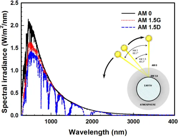
To characterize the solar cell performance, JL – V characteristics are measured under the illumination of air mass (AM) 1.5 conditions which are universally employed like as a standard to characterize the solar cell performance. A solar simulator produces the similar illumination spectrum of AM 1.5. AM defines the optical path length through the atmosphere of Earth. As it travels, the sunlight undergoes the absorption and the scattering
18
by atoms and molecules in the atmosphere. As a result, the intensity of sunlight is attenuated. AM coefficient, which is a number following AM, characterizes the solar spectrum after the solar radiation has traveled through the atmosphere. Figure 1.12 illustrates the spectral irradiance of AM 0 and AM 1.5 as a function of wavelength. AM 0 is the spectrum of sunlight out of Earth’s atmosphere. The AM 1.5G spectrum which is mostly used for the solar cell measurement is for the terrestrial applications. It includes the direct and diffuse light. And it integrates to 100 mW/cm2. The AM 1.5D spectrum is also for terrestrial applications but it includes direct light only. It integrates to 88.8 mW/cm2.
Figure 1.12 – Air mass; solar spectral irradiance as a function of wavelength Inset shows incident angle of sunlight relative to zenith (normal to the earth’s surface).
Chapter 1 – Background knowledge 19 Figure 1.13 – A typical solar cell J‐V curve with solar cell parameters.
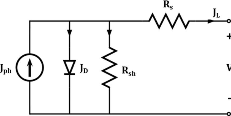
Figure 1.13 illustrates a typical solar cell JL – V characteristic. Important solar cell parameters are noted in the figure. Short‐circuit current density (Jsc) represents the generated current density under AM 1.5 illumination when applied voltage equals zero (V=0, short‐circuited). JL can be ideally expressed as the equation given by 1 (6) where Jph is photo‐current density which depends on the materials, device structures, the power of incident light, etc. However, the practical model of Jsc which contains series (Rs) and shunt (Rsh) resistance can be redefined based on the equivalent circuit model with resistance.
20
Figure 1.14 – Equivalent circuit model of solar cell consisted of constant current source, diode, series and shunt resistance.
Figure 1.14 illustrates an equivalent circuit model of the solar cell. A diode is connected in parallel with Jph (a constant current source) and Rsh. Also it has series connection with Rs. From this equivalent circuit, JL is expressed by
1 (7)
Last term in this equation is called the shunt current which depends on both resistance values. If Rs and Rsh approach to zero and infinity respectively, the diode is the ideal diode. But in general, this shunt current can govern total JL in the inverse case. Open‐circuit current (Voc) is defined as the voltage without current flow in the solar cell (JL=0, open‐circuited). In other words, the same amounts of dark and photo currents flow in reverse direction each other. Voc is given by ln 1 (8)
Chapter 1 – Background knowledge
21
Fill factor (FF) is defined as the ratio of the maximum power (Pmax) to the product of the Jsc and the Voc which is given by the equation in Figure 1.13 inset. FF is always less than 1. FF is severely affected by resistive effects. It means that FF is improved with the increase in Rsh and the decrease in Rs .
The power conversion efficiency (η) is the most effective parameter describing solar cell performance. It is defined as the ratio of energy output from the solar cell to input energy from the sun. η is written as an equation based on the solar cell parameters introduced above.
η
∙ ∙ (9)
where Plight is the power of incident light. Typically, Plight of 100 mW/cm2 is used as a standard.
22
1.5 Hybrid solar cells based on silicon and organic materials
Conventional silicon solar cells based on p‐n junction showed high efficiency about 25 %. However, the high fabrication cost due to crystalline silicon wafer and high temperature process is a barrier for wide use. Organic materials are interesting in terms of fabrication costs because solution processes are possible at room temperature. However, the energy conversion efficiency of organic solar cells is evidently lower (11 %) than silicon based solar cells [46]. Hybrid solar cell is an approach which aims at the low cost and high efficiency solar cell. Basically, there are two kinds of approaches for hybrid solar cells. First, the organic materials are used to improve cost‐efficiency of silicon based solar cells. PEDOT:PSS [20, 47, 48], P3HT [3] and Spiro‐OMETAD [13] are generally deposited by the solution process. Second, many different types of silicon, such as crystalline silicon wafer [49], thin‐films [50], nanocrystals [51], nanorods [13] and nanowires [4, 20, 52], are integrated with organic semiconducting polymers. The silicon materials could improve the efficiency by efficient exciton separation and rapid charge transport (compensation of low mobility of organic materials). The hybrid solar cells based on silicon and organic materials can be classed into three different types according to the main light absorbing material.
Type 1 Type 2 Type 3
Light absorbing material(s) Silicon Organic semiconducting polymer Both Photo‐carrier generation by Electric field in silicon Band energy offset at interface Both Efficiency ~ 10 % 0.1 ~ 1.5 % 2 ~ 6 % Table 1.1 – Summary of types of hybrid solar cells based on light absorbing materials.
Chapter 1 – Background knowledge 23 Table 1.1 summarizes the types of hybrid solar cells and related factors. Type 1 hybrid solar cell employs silicon as the main light absorbing material. Organic materials are used to create the built‐in potential in silicon and to transport photo‐generated carriers. Here, a key point is how many photo‐ generated carriers in silicon can be efficiently collected by the organic material. Therefore, the conductivity of organic material and surface states of silicon are significantly important. Figure 1.15 shows an example of Type 1 solar cells presented by Jeong et al [53]. It bases on silicon nanocone fabricated by the colloidal lithography of n‐type silicon wafer to decrease reflectance of silicon surface. The p‐n junction is formed by depositing PEDOT:PSS by a solution process (Figure 1.15 (a)). The incident light from top side is mainly absorbed by silicon through highly transparent 60 nm thick PEDOT:PSS. Silicon nanocone generates electron‐hole pairs which are separated by the built‐in potential created by PEDOT:PSS [49]. Photo‐ generated holes are transferred from silicon to PEDOT:PSS. It demonstrated high Jsc of 30 mA/cm2. The efficiency reaches 11 % (Figure 1.15 (b)). This approach lowers the cost of fabrication compared to conventional silicon p‐n junction solar cell owing to the solution process at room temperature. Type 1 hybrid solar cells normally show higher efficiency than that of other types due to the use of silicon wafer. Figure 1.15 – The example of type 1 hybrid solar cell based on n‐type silicon nanocone and PEDOTPSS. (a) solar cell structure and (b) solar cell performance (reprinted from Ref. [53])
24
Type 2 hybrid solar cells are used organic semiconducting polymers, which create excitons by light absorption, as a main absorber. Silicon is employed as an electron acceptor. Thus, Type 2 solar cell is an excitonic solar cell [54]. For the high power conversion efficiency, the efficient exciton separation and the carrier transport are important. Figure 1.16 illustrates one of Type 2 solar cells based on P3HT absorber and silicon nanocrystals (SiNCs) reported by Liu et al [51]. The solar cell is constructed like organic bulk‐heterojunction solar cells from the blend of P3HT and SiNCs (Figure 1.16 (a)). Figure 1.16 (b) clearly showed that the absorbance of the blend imitates the absorbance of P3HT. Surely, P3HT plays a role of the main light absorbing material. The excitons generated in P3HT are dissociated at the interface with SiNCs. The solar cell performance is altered by the concentration of SiNCs which is concerned with the interface area, the percolated pathway, the absorption of SiNCs, etc. Despite of low cost process and materials, the efficiency is seriously limited to 1 % (Figure 1.16 (c)). Among solar cell parameters, Jsc is quite lower compared to that of Type 1 hybrid solar cells.
Figure 1.16 – The example of type 2 hybrid solar cells based on P3HT and silicon nanocrystals. (a) solar cell structure (b) absorbance and (c) solar cell performance. (reprinted from Ref. [51])
Chapter 1 – Background knowledge
25
Type 3 hybrid solar cells are also available. Some solar cell devices are not easy to determine main absorber because they employed both silicon and organic material that show the efficient light absorption. In this case, both types’ (Type 1 and 2) characteristics can be observable. It means that the incident light is absorbed in both materials and electron‐holes pair and excitons are generated in silicon and organic semiconducting polymers, respectively. Figure 1.17 shows an example of type 3 hybrid solar cells reported by Zhang et al [3]. P3HT is deposited on nanostructured n‐type silicon wafer by spin‐coating of P3HT dissolved in chlorobenzene with 15 mg/mL concentration. P3HT and silicon wafer carry photo‐generated holes and electrons, respectively. In this paper, P3HT plays a dominant role on the hydrogen terminated silicon surface. But, the efficiency is only 0.006 %. A surface modification of silicon strongly changed the trend of external quantum efficiency. Methyl‐terminated silicon improves power conversion efficiency up to 5.9 % by the efficient collection of photo‐generated holes from silicon. Jsc is considerably raised from 0.031 to 26.2 mA/cm2. Another report on Type 3 hybrid solar cells based on a‐Si:H and organic semiconducting polymers demonstrated lower efficiency (2~3 %) than that of crystalline silicon based solar cells [25, 26]. From this fact, the efficiency might be dominantly governed by silicon part. Figure 1.17 ‐ The example of type 3 hybrid solar cell based on n‐type silicon wafer and P3HT. (a) solar cell structure and (b) solar cell performance (reprinted from Ref. [3])
26
The three different types of hybrid solar cells using silicon and organic materials have been explored. The power conversion efficiency is mostly dependent on the main light absorbing material. The hybrid solar cells based on silicon absorber demonstrated the higher efficiency than that of the hybrid solar cells based on organic polymer absorber. However, the hybrid solar cell based on crystalline wafer should be avoided for the next‐ generation of solar cells due to the cost efficiency. The organic semiconducting polymers could be potential alternatives to silicon absorber. They have advantages of the tuning of molecule by synthesis, the high absorption coefficient and the easy fabrication process. Nevertheless, researches on the hybrid solar cell with organic semiconducting polymer as an absorber still have a long way to go regard to the efficiency improvement and the understanding of device physics.
Chapter 1 – Background knowledge 27
1.6 Approaches of thesis
In this thesis, we investigated the integration of organic semiconducting polymer with PECVD grown SiNWs for a hybrid solar cell application. The hybrid solar cells based on P3HT absorber and SiNWs were fabricated. It is classed as Type 2 hybrid solar cell since P3HT showed dominant light absorption than SiNWs. PECVD grown SiNWs by Sn or Bi catalysts clearly showed the difference in their nano‐morphology. According to their morphologies, hybrid solar cells are designed with the different role of SiNWs.First, we explored the potential application of SiNWs as light trapping media. In this purpose, the blend of P3HT and PCBM was spin‐coated on Sn‐ catalyzed SiNWs as an organic light absorbing material. The nanowires are not concerned in exciton dissociation because they are separated from the organic active layer by PEDOT:PSS. The SiNWs mainly concern with the light trapping and the extraction of photo‐generated holes from the organic layer. Particularly, the correlation of the quality of SiNWs with solar cell performances in optical and electrical aspects is focused in Chapter 4.
Second, the investigations on hybrid heterojunction were performed based on P3HT and Bi‐catalyzed and Bi‐doped SiNWs. The ideal structure (large area of interface and electron/hole transport pathway) is available due to the nanostructure given by the SiNWs. Since Bi‐catalyzed SiNWs exhibited the electrical n‐type nature, they were employed as an electron acceptor to take electrons from P3HT. The exciton dissociation would be a key role of Bi‐catalyzed SiNWs. The solar cell performance is discussed in Chapter 5.
28
R
EFERENCE1. Chapin, D.M., C.S. Fuller, and G.L. Pearson, A New Silicon p‐n Junction
Photocell for Converting Solar Radiation into Electrical Power. Journal of
Applied Physics, 1954. 25(5): p. 676‐677.
2. Liu, C.‐Y., Z.C. Holman, and U.R. Kortshagen, Optimization of Si NC/P3HT
Hybrid Solar Cells. Advanced Functional Materials, 2010. 20(13): p. 2157‐
2164.
3. Zhang, F.T., et al., Air Stable, Efficient Hybrid Photovoltaic Devices Based on
Poly(3‐hexylthiophene) and Silicon Nanostructures. Chemistry of Materials,
2011. 23(8): p. 2084‐2090.
4. Kuo, C.Y. and C. Gau, Arrangement of band structure for organic‐inorganic
photovoltaics embedded with silicon nanowire arrays grown on indium tin oxide glass. Applied Physics Letters, 2009. 95(5): p. 053302‐3.
5. Golap, K. and et al., Silicon nanowire array/polymer hybrid solar cell
incorporating carbon nanotubes. Journal of Physics D: Applied Physics,
2009. 42(11): p. 115104.
6. Garnett, E.C., et al. Silicon nanowire hybrid photovoltaics. in Photovoltaic
Specialists Conference (PVSC), 2010 35th IEEE. 2010.
7. Garnett, E.C. and P. Yang, Silicon Nanowire Radial p−n Junction Solar Cells. Journal of the American Chemical Society, 2008. 130(29): p. 9224‐9225. 8. Tsakalakos, L., et al., Silicon nanowire solar cells. Applied Physics Letters,
2007. 91(23): p. 233117‐3.
9. Syu, H.‐J., S.‐C. Shiu, and C.‐F. Lin, Silicon nanowire/organic hybrid solar cell
with efficiency of 8.40%. Solar Energy Materials and Solar Cells, 2012. 98(0):
p. 267‐272.
10. Davenas, J., et al., Silicon nanowire/poly(3‐hexylthiophene) hybrids for thin
film solar cells. Journal of Non‐Crystalline Solids, 2012. 358(17): p. 2534‐
2536.
11. Th, S. and et al., Silicon nanowire‐based solar cells. Nanotechnology, 2008. 19(29): p. 295203.
12. Cho, J., et al., Sn‐catalyzed silicon nanowire solar cells with 4.9% efficiency
grown on glass. Progress in Photovoltaics: Research and Applications, 2012:
13. He, L., et al., Highly efficient Si‐nanorods/organic hybrid core‐sheath
heterojunction solar cells. Applied Physics Letters, 2011. 99(2): p. 021104‐3.
14. Huynh, W.U., J.J. Dittmer, and A.P. Alivisatos, Hybrid Nanorod‐Polymer Solar
Cells. Science, 2002. 295(5564): p. 2425‐2427.
15. Qu, Y. and X. Duan, One‐dimensional homogeneous and heterogeneous
nanowires for solar energy conversion. Journal of Materials Chemistry, 2012.
![Figure 1.4 – Density of state of hydrogenated amorphous silicon. Exponential band tail states and deep states are illustrated [27].](https://thumb-eu.123doks.com/thumbv2/123doknet/2995656.83992/27.892.258.624.732.1054/figure-density-hydrogenated-amorphous-silicon-exponential-states-illustrated.webp)
![Figure 1.16 – The example of type 2 hybrid solar cells based on P3HT and silicon nanocrystals. (a) solar cell structure (b) absorbance and (c) solar cell performance. (reprinted from Ref. [51])](https://thumb-eu.123doks.com/thumbv2/123doknet/2995656.83992/45.892.166.757.693.1016/figure-example-silicon-nanocrystals-structure-absorbance-performance-reprinted.webp)