0
République Algérienne Démocratique et Populaire
Ministère de l’Enseignement Supérieur et de la Recherche Scientifique
Université Ferhat Abbas–Setif
THESE
Présenté à la Faculté des Sciences
Département de Physique
Pour l‟obtention du diplôme de
DOCTORAT EN SCIENCES
Spécialité : Physique énergétique
Par
Azzouzi Ghania
THEME
STUDY OF SILICON SOLAR CELLS PERFORMANCES
USING THE IMPURITY PHOTOVOLTAIC EFFECT
Soutenue Publiquement le 03/03 /2012
Devant la commission d‟examen :
Président : Mr A. Layadi Professeur (Université Ferhat Abbas– Sétif)
Rapporteur: Mr M. Chegaar Professeur (Université Ferhat Abbas– Sétif)
Examinateur:M
meC. Azizi Professeur (Université Oum labouaghi)
Examinateur:Mr A. Bouabellou Professeur (Université Constantine)
1
Acknowledgements
It has been a long journey finishing this thesis and it would have been much harder without the aid of many excellent people.
First, I thank Pr Mohamed Chegaar for being my thesis supervisor all these years.
This thesis would not have been possible without the generous assistance of Pr Abdelhamid Layadi who has been a tireless source of encouragement, support and wisdom over these last years.
My gratitude also goes to the members of the jury who accepted to examine and evaluate my work. I thank heartily Mr A. Layadi Pr at Ferhat Abbas University who accepted to preside the jury. I thank greatly Mr A. Bouabellou, Pr at Mantouri (Constantine) university and many thank to Meme C. Azizi Pr at Larbi ben Mhidi (Oum Labouaghi) University who honoured me by their acceptation to examine my thesis.
I must thank Mr Marc Burgelman from University of Gent (Belgium) for offering me the opportunity to use the Scaps Simulator and for email responses clarifying and explaining about details of IPV effect and SCAPS.
My thanks also go to Pr. Pierre Mialhe from Via Domitia University (Perpignan – France) for his kindness and patience given to me throughout the duration of my training period in France.
Finally, I thank my parents, my brothers , my sisters and my friends for their endless love and support that have made the hard times so much easier.
2
Table of contents
ACKNOWLEDGEMENTS ... 1
GENERAL INTRODUCTION ... 5
CHAPTER ONE :PRINCIPLES OF SOLAR CELLS ... 6
I.1INTRODUCTION ... 7
I.2 Solar Spectrum ... 7
I.3 Basic Principles of a Solar Cell ... 8
I.4SOLAR CELL CHARACTERISTICS ... 12
I.4.1 Short Circuit Current Isc ... 12
I.4.2 Open Circuit Voltage ... 12
I.4.3 Fill Factor FF ... 13
I.4.4 Efficiency ... 13
I.5LOSSES IN SOLAR CELLS ... 13
I.5.1 Loss of Low Energy Photons: ... 13
I.5.2 Thermalization Loss (loss due to excess energy of photons)... 13
I.5.3 Voltage loss ... 14
I.5.4 Fill Factor Loss ... 14
I.5.5 Reflection losses: ... 15
I.5.6 Loss by Incomplete Absorption due to the Finite Thickness ... 15
I.5.7 Loss Due to Metal Coverage ... 15
I.5.8 Recombination losses ... 15
I.6MODEL OF A SOLAR CELL ... 15
I.6.1 Ideal Solar Cell ... 15
I.6.2 Real Solar Cell ... 18
I.7QUANTUM EFFICIENCY AND SPECTRAL RESPONSE ... 21
I.8SOLAR CELL MATERIALS AND DIFFERENT GENERATIONS ... 22
I.8.1 Technology Generation ... 22
I.8.2 Photovoltaic Materials ... 23
I.8.2.1 Silicon ... 24
I.8.2.2 Cadmium Telluride (CdTe) ... 25
I.8.2.3 Copper-Indium Selenide (CuInSe2) ... 26
3
I.8.2.5 Light-absorbing Dyes ... 28
I.8.2.6 Organic/Polymer Solar Cells ... 29
I.8.2.7 Nano-crystalline Solar Cells ... 29
I.9TECHNOLOGIES FOR THE REDUCTION OF EFFICIENCY LOSSES ... 32
I.9.1 Technologies for the Reduction of Optical Losses (light confinement) ... 32
I.9.2 Technologies for the Reduction of Losses Due to Recombination ... 36
I.10CONCLUSION ... 46
References ... 47
Chapter Two :Third Generation Solar Cells ... 49
II.1INTRODUCTION ... 50
II.2 Shockley Queisser Limit ... 50
II.3 Price and Efficiency Projections for Solar Cell Generations... 51
II.4DIFFERENT THIRD GENERATION SOLAR CELLS ... 52
II.4.1 Multiple Junction (MJ) Solar Cells (Tandem Solar Cell) ... 53
II.4.2 Spectrum Conversion Solar Cells: Down and Up Conversion ... 55
II.4.3 Hot Carrier Solar Cells ... 58
II.4.4 Intermediate-band solar cells ... 60
II.4.5 Impurity Photovoltaic Effect ... 63
II.4.5.1 Introduction ... 63
II.4.5.2 Theory of the IPV Effect ... 65
II.4.5.3 Requirements for the IPV Effect ... 67
II.5CONCLUSION ... 73
References ... 74
CHAPTER THREE :SCAPSSIMULATOR,RESULTS AND DISCUSSION ... 77
III.1INTRODUCTION ... 78
III.2 Part I: SCAPS Simulator: ... 78
III.2.1 Principal Operations and Main Panels ... 78
III.2.1.1 Define the working point ... 79
III.2.1.2 Select the Measurement(s) To Simulate ... 81
III.2.1.3 Define the problem ... 81
III.2.2 General Remark on Defects and Recombination: ... 82
4
III.3 Part II: results and discussion ... 85
III.3.1 Introduction ... 85
III.3.2 Aim of the study ... 86
III.3.3 Silicon solar cell structure and physical parameters used in the simulation ... 86
III.3.4 Results and Discussion ... 88
III.4CONCLUSION ... 94
References ... 94
5
General Introduction
The very important goal nowadays is to find a new renewable form of energy. The renewable sources of energy derived from the sun are one of the promising options. Extensive studies on the photovoltaic cell as one of a renewable energy sources have been carried out in order to obtain cheap PV cells that are more efficient and safe.
The most important loss mechanisms in single band gap cells are the incapability to absorb photons with energy less than the band gap and thermalization of photon energy exceeding the band gap. The third generation solar cells have attracted wide attention in these last years, the concepts of this generation are still under fundamental investigation and are based on tackling one or both of the previous loss mechanisms in order to increase cell conversion efficiency. The impurity photovoltaic effect (IPV) is one of these concepts. It can, improve the conversion efficiency of a conventional single junction solar cell by the incorporation of optically active impurities into the device. These impurities permit electrons to be excited from the valence band to the conduction band via the defect level through the absorption of sub-band-gap photons.
The work presented in this thesis is focused on attempts to develop the efficiency of the silicon solar cell above the Shockley-Queisser efficiency limit through the IPV effect. We investigate numerically the potential of the IPV effect in silicon solar cell doped with sulphur as novel IPV impurity. The influences of light trapping and certain impurity parameters like impurity concentration and position in the gap on the silicon solar cell performances (Short circuit current density Jsc, open circuit voltage Voc, conversion efficiency η and quantum efficiency QE) were studied.
In chapter I, the essential principles of a solar cell, the main concepts and materials used for making solar cells, the efficiency loss mechanisms in PV cells and how to reduce or overcome these losses will be explicated. In the present day there are many attempts to invent and develop new concepts aimed to obtain high efficiency over the present limit. Chapter II will describe in detail many classes of these concepts and will further explain in more detail the impurity photovoltaic effect which is the purpose of our study. Chapter III comprises two parts: in the first part, a detailed description will be given of the Solar Cell Capacitance Simulator in one Dimension (SCAPS-1D) that is used in this work. In part two, the most significant results and discussion of the study will be presented.
6
Chapter One
7
I.1 Introduction
This chapter lays out the theoretical foundations on which the analyses in this thesis are based. First, some notions about the sun as source of energy will be presented. Than, we will present the basic principles of a solar cell, the principal materials used in this field, the efficiency losses mechanisms in solar cells and the methods used to reduce these losses will be also analysed.
I.2 Solar Spectrum
The study of solar cells (progress, optimization and characterization….etc.) need some information about the source of energy used; the sun. This star is the biggest member of the solar system. The sun is a big sphere of plasma composed of H and He and some small amounts of other elements, it has an effective black-body temperature TS of 5777 K. The diameter of the sun is around 1.39x10⁹ m and the distance between it and the earth is about 1.5x10¹¹ m. The solar radiation is partially absorbed and scattered by its passage through the atmosphere. The absorption of the X–rays and extreme ultraviolet radiations of the sun is principally caused by nitrogen and oxygen while the absorption of the ultraviolet (λ<0.40 μm) and infrared radiations (λ>2.3 μm) is mainly caused by the ozone and water vapors. The atmosphere of the earth absorbs the ultraviolet (UV) and far infrared radiation and allows only short wavelength radiation (i.e. between 0.29 μm and 2.3 μm). It does not permit radiation having wavelength λ>2.3 μm, (i.e. long wavelength radiation) [1]. Figure (I-1) shows the solar spectrum as a function of photon energy. The terms AM0 and AM1.5 used in this figure are the designations of a particular radiation conditions. The concept „Air Mass
(AM)‟ represents the amount of atmosphere through which the solar radiation has travelled
and is correlated to the amount of absorption.
AM 1/ cos (θ
The θrepresents the angle of the sun to the vertical.Outside the atmosphere the spectrum is
AM0 and that on the surface of the earth for normal incidence is AM1. The spectrum AM1.5
8 This energy spectrum is regarded as the standard spectrum for measuring the efficiency of PV cells used for terrestrial applications.
Figure I-1: Solar spectrum for different Air Mass and blackbody radiation corresponding to the sun.
I.3 Basic Principles of a Solar Cell
The photovoltaic effect was first observed by Henri Becquerel [2] in 1839. This phenomenon is the basic physical process in which a solar cell converts solar energy to electricity. In a global sense, the device intended to capture solar and non solar radiation is usually known as solar cell. Verily, this device require to realise two steps: the first, is the photogeneration of charge carriers (electrons and holes) and secondly the separation of these carriers to a conductive contact that will transmit the electricity. Currently, the majority of solar cells in use are silicon semi-conductor junction devices. Therefore, in order to study the photovoltaic cells we must have an understanding of the basics of the semi-conductor materials and particularly the PN junction, although, PN junctions and semiconductors are not
9 the only principles and materials to understand photovoltaic cell. Many materials, mechanisms and new concepts have been studied in the last years (see chapter 2).
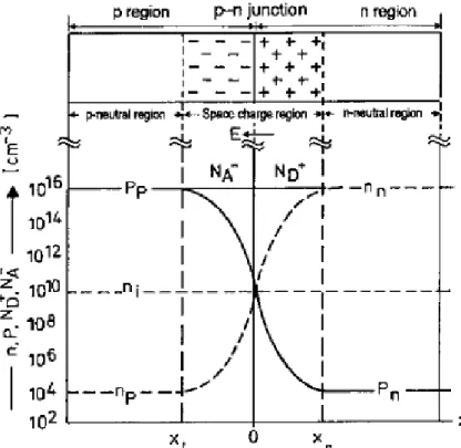
To recognize the function of semiconductor devices and therefore, of solar cells, it necessary to understand deeply, the processes within a p-n junction is important. The semiconductor junction is generally the base unit of many PV cells, in which two different dopants directly adjoin one another. This is called a p-n junction if a p-doped layer merges into an n-doped layer within the same lattice. In a simple example, we assume that – in silicon – both dopants are of the same magnitude and merge together abruptly. Figure I-2 may clarify this behaviour. The left-hand side x < 0 would, for example, be doped with boron atoms with a concentration of NA = 1016 atoms per cm−3, making it p-conductive. The right-hand side x > 0, on the other hand, could be doped with phosphorus atoms, at ND = 1016 cm−3, making it n-conductive. The freely moving charge carriers will not follow the abrupt change in concentration from NA to ND. Rather, the carriers will diffuse due to the difference in
concentration, i.e., the holes from the p region will move into the n region, and the electrons from the n area will move into the p region. Diffusion currents will arise. The ionized acceptors and donors, which are no longer electrically compensated, remain behind as fixed space charges (Figure I-2). Negative space charges will arise on the left-hand side in the p region, and positive space charges arise on the right-hand side in the n region. Correspondingly – as occurs in a plate capacitor – an electric field is created at the p-n junction, which is directed so that it drives the diffusing charge carriers in the opposite direction to the diffusion. This process continues until equilibrium is created or, in other words, until the diffusion flow is compensated by a field current of equal magnitude. An (extremely large) internal electric field exists – even if both sides of the semiconductor are grounded. When the p-n junction is illuminated, charge carrier pairs will be generated wherever light is absorbed. The strong field at the junction pulls minority carriers across the junction and a current flow results. The semiconductor device is not in thermal equilibrium, which means that electric power can be delivered to a load. This is the basic mechanism of a solar cell[3]. A typical such solar cell according to Figure I-3 consists of a p-n junction, which has a diode characteristic. This characteristic can be derived from standard solid state physics. It is: 0 T 1 A V V e I I (I-2)
The I is the current through the diode at applied voltage VA. VT is a constant, the so-called thermal voltage. I0 is the diode saturation current, which depends on the type, doping density,
10 and quality of the semiconductor material and the quality of the p-n junction. If this junction is illuminated, a supplementary current, the light-generated current Iph is added: than the
equation I-2 becomes
ph V V I e I I T A 0 1 Or 0 k T 1 qV ph B e I I I (I-3)
The kB is the Boltzmann constant, T is the absolute temperature, q (>0) is the electron charge,
and V is the voltage at the terminals of the cell. I0 is well known to electronic device
engineers as the diode saturation current serving as a reminder that a solar cell in the dark is simply a semiconductor current rectifier, or diode. The photogenerated current Iph is closely related to the photon flux incident on the cell and its dependence on the wavelength of light is frequently discussed in terms of the quantum efficiency or spectral response. The photogenerated current is usually independent of the applied voltage with possible exceptions in the case of a-Si and some other thin film materials [4-6].
Figure I-2: Doping and concentration distribution of a symmetrical p-n junction in thermal equilibrium.
11
Figure (I-3) Operation mechanism of single-crystal silicon p-n junction solar cell.
The negative sign in equation (I-3) results from polarity conventions. Now the current I is no longer zero at zero voltage but is shifted to Iph. Power can be delivered to an electric load. The
I-V characteristic with and without illumination is shown in Figure I-4.
12
I.4 Solar Cell Characteristics
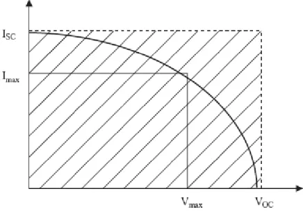
PVcells are usually characterised with four performances: short circuit current Isc, open circuit voltage Voc, fill factor FF, and conversion efficiency η. These parameters can be represented using Figure (I-5). The curve drawn in figure (I-5) is same as illuminated curve shown in figure (I-4), but negative current axis is shown as positive, this signification is done for the sake of convenience.
Figure I-5 Typical plot of a solar cell‟s I-V curve and its parameters.
I.4.1 Short Circuit Current Isc
The short-circuit current is the current through the solar cell when the voltage across the solar cell is zero (i.e., V=0). When we put V=0 in equation I-3 we obtain the short circuit current as Jsc =-Iph. The Isc is usually represented in terms of current density and current per unit area in terms of mA/cm2.
I.4.2 Open Circuit Voltage
The open circuit voltage is the maximum possible voltage generated across the terminals of a solar cell when they are kept open, i.e., I=0 (Figure I-5).
13 I.4.3 Fill Factor FF
The fill factor is defined as the ratio of maximum power Pm Vm.Im that can be
extracted from a solar cell to the ideal power P0 Voc.Isc . So,
sc oc m m I V I V FF . . (I-4)
The FF is a key parameter in evaluating the performance of solar cells. It is represented in terms of percentage.
I.4.4 Efficiency
The conversion efficiency is the most important property of a solar cell. It is defined as the ratio between the generated maximum power, Pm, generated by a solar cell and the incident power, Pin. in oc sc in m m in m P V I FF P V I P P . . (I-5)
I.5 Losses in Solar Cells
The conversion efficiency of a real solar cell is generally lower than that of an ideal solar cell due to the various loss factors, some of these are avoidable but others are intrinsic to the system. Schematic presentation of the important loss mechanisms in solar cells is presented in Figure I-6 and these factors are:
I.5.1 Loss of Low Energy Photons:
In the solar cell a significant part of the solar spectrum is not utilised because of the incapability of the material to absorb the photons which have energy less than the band gap energy. Therefore, these photons do not contribute to the generation of electron hole pairs. This is referred to as “transmission loss”, and is almost equal to 23% for a single junction solar cell.
I.5.2 Thermalization Loss (loss due to excess energy of photons)
A photon which have energy equal to that of the band gap energy is needed to excite an electron from valance band to conduction band. If the energy of the absorbed photons E is
14 larger than the band gap energy Eg, the excess energy E-Eg is dissipated into lattice vibrations within a picoseconds. This loss is referred to as thermalization loss. For a single junction solar cell, this loss is equal to about 33%.
I.5.3 Voltage loss
The voltage factor is the ratio of the maximum voltage Voc developed by the cell to the band gap voltage Eg/q. This loss happens due to the unavoidable intrinsic Auger recombination. The ration Voc/ (Eg/q) lies in the range of 0.65 to 0.72 for a thick silicon solar cell.
I.5.4 Fill Factor Loss
The fill factor FF describes the squareness of the IV curve. If the FF is equal to one, the (I-V) curve of an ideal solar cell is square. In reality, the cell I-V curve is given by the exponential behaviour. This form of loss appears from the parasitic resistances (series and shunt resistance) of the cell.
15 I.5.5 Reflection losses:
The reflection loss occurs from the top surface of the PV cells. A part of incident photons are reflected from this surface and not absorbed.
I.5.6 Loss by Incomplete Absorption due to the Finite Thickness
Incomplete absorption in the absorber due to its limited thickness is an additional loss that reduces the efficiency of the energy conversion. It refers to the loss of photons which has enough energy to be absorbed in the cell, but can not absorbed in the cell by reason of limited solar cell thickness. The incomplete absorption is becoming important in the current when the wafer becomes thinner in order to save the active material for cost reduction purpose. Light trapping methods are generally used to reduce this loss.
I.5.7 Loss Due to Metal Coverage
The front contact of the solar cell is made by the form of finger, and busbar. This metal contact shadows some light. This loss is equal to about 10%.
I.5.8 Recombination losses
Not all the generated (electron – hole) pairs contribute to solar cell current and voltage due to recombination. The carriers recombine in the bulk, at the interfaces, and/or at the surfaces of the junction. Many techniques are used to minimize several recombination problems including passivation techniques.
The optical and electrical losses mentioned above should be minimized in order to get high solar cell characteristics. Many methods and techniques can be used for reducing efficiency losses. In the last two sections, these methods will be described in detail.
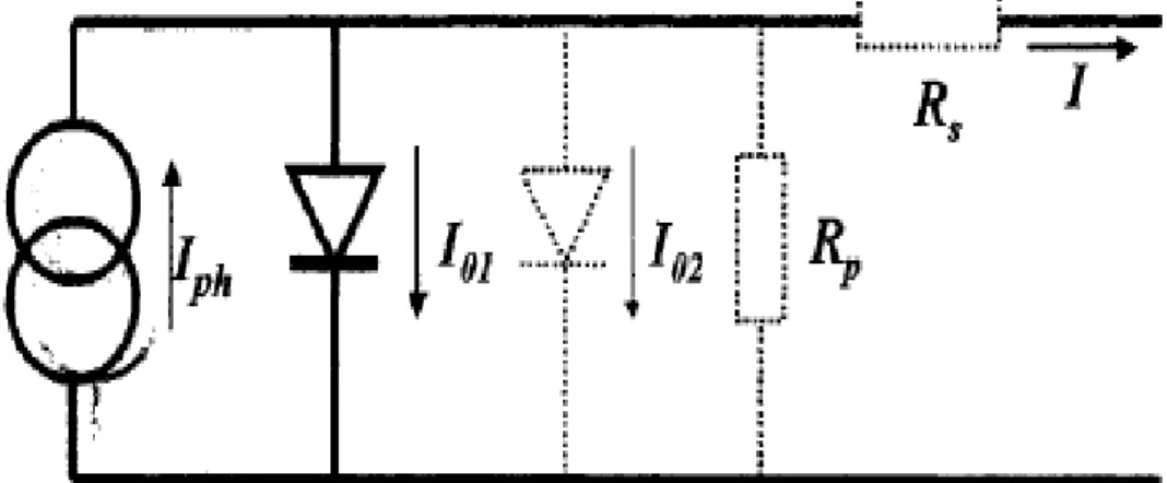
I.6 Model of a Solar Cell
I.6.1 Ideal Solar CellAn ideal solar cell can be considered as current source connected in parallel with a rectifying diode, as shown in the equivalent circuit of Figure I-7. The I-V characteristic is described by the Shockley solar cell equation (equation (I-3)):
16 0 kT 1 qV ph B e I I I
The term I0 represents the the diode saturation current. kB represents the Boltzmann constant, T is the absolute temperature, q : is the electron charge, and V is the voltage at the terminals of the cell and Iph is the photogenertated current.
Figure I-7: The equivalent circuit of an ideal solar cell (full lines). Non-ideal components are shown by the dotted line.
Figure I-8(a) shows the I-V characteristic (Equation (I-3)). For the ideal solar cell, the short circuit current Isc is equal to the photogenerated current Iph,
Open circuit voltage is obtained by setting I=0 in the expression for overall current i.e. I=0 when V=Voc. Therefore, the open circuit voltage Voc is given by equation
0 1 ln I I q T K Voc B ph (I-6)
The power P = I V produced by the cell is shown in Figure I-8 (b). The cell generates the maximum power Pmax at a voltage Vm and current Im, and it is convenient to define the fill factor FF by oc sc oc sc m m V I P V I V I FF m ax (I-7)
17 The fill factor FF of a solar cell with the ideal characteristic will be furnished by the subscript
0(i.e. FF=FF0 in the absence of any parasitic resistance) as given by the approximate
expression [7]
1 72 . 0 ln 0 oc oc oc FF (I-8)a
b
Figure I-8. The I-V characteristic of an ideal solar cell (a) and the power produced by the cell (b). The power generated at the maximum power point is equal to the shaded
18 I.6.2 Real Solar Cell
The behaviour of a real solar cell is deviated from the ideal due to electrical and optical losses. The I-V equation of equivalent circuit (Figure I-7) of real solar cell can be written in the form of the following equation.
Rp IRs V T K RsI V I T K IRs V I I I B B ph 1 1 2 exp 1 exp 02 01 (I-9)
The form of this equation is called “two-diode model”. The term I01 and I02 represent the saturation current densities. The first term represents the recombination in the base and emitter of the cell. While I02 represents the recombination in the space charge region of the cell. The real solar cell (or circuit) may also contain series (Rs) and parallel (or shunt, Rp or
(Rsh)) resistances. The series resistance arises from the bulk resistance of the silicon wafer, the resistance of the metallic contacts of the front- and back surface and further circuit resistances from connections and terminals. The parallel resistance is principally caused by leakage currents by reason of p-n junction non-idealities and impurities near the junction, which cause partial shorting of the junction, particularly near the cell edges. These parameters are shown in the equivalent circuit of Figure (I-7) by the dotted lines.
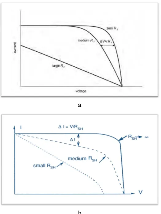
Influence of Shunt and Series Resistances on Solar cell Efficiency
The effect of the series and parallel resistances, on the I-V characteristic of the solar cell is shown in Figures I-9 (a and b). The series and shunt resistances affect mainly the fill factor and therefore affect the efficiency of the solar cell. The influence of these parameters on the fill factor can be written as
rs
FF FF 0 1 (I-10) Where, oc sc s V I Rs r . . And sh r FF FF 0 1 1 (I-11)19 Where, oc sc sh sh V I R r .
The fill factor indicates how well a junction was made in the cell and how low the series resistance was. Preferably the value of Rsh must be very large, in range of hundred Ohms. Only larger series resistances reduce the short-circuit current but very small shunt resistances reduce the open-circuit voltage. However, their effect reduces mainly the value of the Fill factor. Therefore, the maximum power output is decreased.
It must also be taken into consideration, other parameters such as radiation intensity and temperature which also affect the efficiency of a solar cell.
a
b
Figure I-9 The effect of series (a) and parallel (b) resistance on the I-V characteristic of the solar cell.
20 Temperature and Insolation Effects
For practical uses, solar cells do not operate under standard conditions (1000w/m2,
AM1.5global spectrum, 25°C). Two important effects that must be taken into account are due
to the variable temperature and insolation level.
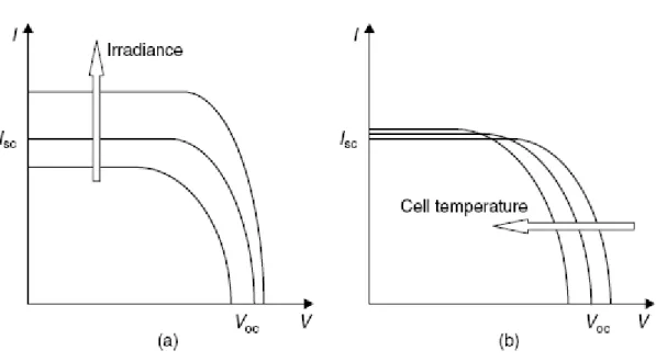
The I-V characteristic of the solar cell, presented in Figure I-8(a), is only for a certain irradiance, Gt, and cell temperature T. The I-V curve in figure I-10, is plotted to demonstrate the influence of these two parameters on the cell characteristic. As shown in Figure I-10(a), the open circuit voltage increases logarithmically by increasing the solar radiation, while the short circuit current increases linearly. The influence of cell temperature on the cell characteristics is shown in the Figure I-10(b). The most significant effect of the increase in cell temperature is on open circuit voltage, which decreases with increasing temperature; thus the cell efficiency decreases. The temperature variation of the current is less marked.
Figure I-10 influence of irradiation and cell temperature on PV cell characteristics (a) Effect of increased irradiation. (b) Effect of increased cell temperature.
21
I.7 Quantum Efficiency and Spectral Response
The quantum efficiency of a solar cell is defined as the ratio of the number of carriers collected by the PV cell to the number of photons of a given energy incident on the solar cell. One can define external and internal quantum efficiencies (designated by EQE(λ) and IQE(),
respectively). They are different in the treatment of photons reflected from the cell: For the value of EQE all photons impinging on the cell surface are taken into account, however, for the value of IQE just photons that are not reflected are considered. The QE is given as a function of either wavelength or energy. If the internal quantum efficiency is identified, the total photogenerated current is given by
d IQE R q Iph
1 (I-12)The Φ(λ) represents the photon flux incident on the cell at wavelength , R(λ) is the reflection
coefficient from the top surface. In an ideal case, Quantum efficiency has a square shape, in which the QE value is fairly constant across the entire spectrum of wavelengths measured. In general, the QE of solar cells is reduced due to some factors like the effect of recombination, in which charge carriers are not capable of move into an external circuit. The same mechanisms that affect the collection probability also affect the QE. For example, modifying the front surface of a PV cell can affect carriers generated near the surface. A quantum efficiency curve for silicon solar cell is shown in Figure I-11 [8].
The spectral response SR(λ) of a solar cell permits an examination of how photons of different wavelengths contribute to the short circuit current. The SR (λ) is defined as the ratio of the photocurrent generated by a solar cell under monochromatic illumination of a given wavelength, to the value of the spectral irradiance at the same wavelength. The SR (λ) is given by [9]:
QE QE hc q SR( ) 0.808. . (I-13)Spectral response in equation (I-13) can be either internal or external, depending on which value is used for the quantum efficiency.
22 Figure I-11 The quantum efficiency of a silicon solar cell.
I.8 Solar Cell Materials and Different Generations
I.8.1 Technology Generation
According to M. A. Green‟s classification there are three major classes of solar cells (first, second and third generation). His classification is based on the nature of the material, the maximum efficiency reachable, and the cost of each type. There are a lot of researches into all these types but the first-generation technologies are dominant in the commercial production, accounting for 89.6% of 2007 production[10].
I.8.1.1 First Generation
First-generation cells consist of large-area, high-quality and single junction devices. These cells are usually made using a silicon wafer. The highest conversion efficiencies
23 obtained up to now are in first generation PV cells. Single junction silicon devices are approaching the theoretical limiting efficiency of 33, 2%.
I.8.1.2 Second Generation
This generation is considerably cheaper to produce than first generation cells; low cost is associated with the use of such though they have lower efficiencies. The most successful second-generation materials are cadmium telluride (CdTe), copper indium gallium selenide, amorphous silicon and micromorphous silicon. These technologies do hold promise of higher efficiencies and offer cheaper production costs.
I.8.1.3 Third Generation
Principally, Third-generation technologies aim to improve poor electrical performance of second-generation thin-film technologies and keep the low production costs. Recent research has marked conversion efficiencies of 30–60% while retaining low cost materials and manufacturing techniques [11]. In order to achieve these high efficiencies, many concepts have studied in this last years such as intermediate solar cell, tandem solar cell, up and down conversion, impurity photovoltaic effect….etc (each of these approaches will be described in detail in chapter 2).
I.8.2 Photovoltaic Materials
The previous generations of technologies are made of various materials and with different structures in order to diminish the cost and reach maximum efficiency. Many types of solar cell material can be distinguished; single crystal, polycrystalline and amorphous silicon, compound thin-film materials and other semi-conductor absorbing layers.
The most popular type of Photovoltaic cells is made of crystalline silicon, while this type is expensive. The amorphous silicon thin-film solar cells are less expensive. The efficiency of an a-Si module is about 6–8% [12]. A variety of compound semi-conductors can furthermore be used to fabricate thin-film solar cells. These compound materials are CuInSe2,
24 I.8.2.1 Silicon
After oxygen, the silicon is the most abundant element in the earth‟s crust; it constitutes about 26% of this crust. It is never occurs free in nature, but in combination with oxygen forming oxides and silicates. In addition to the previous properties, silicon is a non toxic and stable element. It has dominated the majority semi-conductor applications for a long period. Elemental silicon is used in photovoltaic as the main semiconductor material converting light to electricity. The most prevalent bulk material for solar cells is crystalline silicon. Crystalline silicon panels are the most expensive. Bulk silicon is classified into several categories according to crystallinity and crystal size in the resulting ingot, ribbon or wafer [12].
1. Monocrystalline silicon (c-Si): Often made using the Czochralski process. Single-crystal wafer cells tend to be expensive and, because they are cut from cylindrical ingots, do not completely cover a square solar-cell module without a substantial waste of refined silicon. Therefore, generally mono-crystalline panels have uncovered gaps at the four corners of the cells.
2. Poly- or multicrystalline silicon (poly-Si or mc-Si): is produced using of cast square ingots – large blocks of molten silicon carefully cooled and solidified. Mc-silicon cells are cheaper to produce than single-crystal cells but are less efficient (around 12%). Polycrystalline silicon wafers are made by wire-sawing block-cast silicon ingots into very thin (180 to 350 micrometre) slices or wafers. The wafers are usually lightly p-type doped. To make a solar cell from the wafer, a surface diffusion of n-p-type dopants is performed on the front side of the wafer. This forms a p-n junction a few hundred nanometres below the surface.
3. Ribbon silicon: formed by drawing flat thin-films from molten silicon and having a multicrystalline structure. These cells have lower efficiencies than poly-Si, but save on production costs due to a great reduction in silicon waste, as this approach does not require sawing from ingots.
Silicon thin-films are mainly deposited by chemical vapour deposition (typically plasma-enhanced (PE-CVD)) from silane gas and hydrogen gas. Depending on the deposition‟s parameters, this can yield:
1. amorphous silicon (a-Si or a-Si:H) 2. protocrystalline silicon or
25 These types of silicon present dangling and twisted bonds, which results in deep defects as well as deformation of the valence and conduction bands. The solar cells made from these materials tend to have lower energy conversion efficiency than bulk silicon, but are also less expensive to produce. The quantum efficiency of thin-film solar cells is also lower due to the reduced number of collected charge carriers per incident photon. Amorphous silicon has a higher band gap (1.7 eV) than crystalline silicon (c-Si) (1.1 eV), which means it absorbs the visible part of the solar spectrum more strongly than the infrared portion of the spectrum. As
nc-Si has about the same band gap as c-Si, the two materials can be combined in thin layers,
creating a layered cell called a tandem cell. The top cell in a-Si absorbs the visible light and leaves the infrared part of the spectrum for the bottom cell in Nanocrystalline Si.
Recently, solutions to overcome the limitations of thin-film crystalline silicon have been developed. Light trapping schemes, where the incoming light is obliquely coupled into the silicon and the light traverses the film several times, enhance the absorption of sunlight in the films. Thermal processing techniques enhance the crystallinity of the silicon and pacify electronic defects. Despite the several attempts at making better solar cells by using new materials, the reality is that the photovoltaic market is still dominated by solar cells based on silicon wafer.
I.8.2.2 Cadmium Telluride (CdTe)
Cadmium telluride has a direct band gap (about 1.45eV) which enables it to convert solar energy into electricity more efficiently than the indirect band gap semiconductors. It is an efficient light-absorbing material for thin-film solar cells. CdTe is easier to deposit and more appropriate for large-scale production. In 2008, CdTe modules accounted for over 6% of the word production, more than any other thin film technology. In addition their conversion efficiencies of around 11% look set to advance towards 15% in the next few years [13]. Despite the toxicity of CdTe-based solar cells, this is the only technology (except for amorphous silicon) that can be delivered on a large scale.
The toxicity of CdTe is derived from the toxicity of elemental cadmium, a heavy metal that is a cumulative poison. Many studies, principally by researchers of the National Renewable Energy Laboratories (NREL) in the USA, have shown that the release of cadmium to the atmosphere is lower with CdTe-based solar cells than with silicon photovoltaics and other thin-film solar cell technologies [14].
26 The main layers in these thin films solar cells are a transparent top contact, a
CdS/CdTe heterojunction and absorber, and a metallic back contact as shown in Figure
(I-12). A suitable supporting substrate of glass, metal or plastic depending on the rigidity or flexibility of the cell is necessary.
Figure I-12 CdTe solar cell structure.
I.8.2.3 Copper-Indium Selenide (CuInSe2)
The materials based on CuInSe2 that are of interest for photovoltaic applications take into account several elements from Groups I, III and VI in the periodic table. These semi-conductors are particularly attractive for thin-film solar cell applications because of their high optical absorption coefficients and versatile optical and electrical characteristics.
The basic structure of a Cu(In,Ga)Se2 thin-film solar cell is shown in Figure(I-13). The most common substrate is soda-lime glass of 1–3 mm thickness. This is coated on one
27 side with molybdenum (Mo) that serves as metal back contact. The Cu(InGa)Se2 is deposited on top of the molybdenum back electrode as a PV absorber material. The heterojunction is then completed by chemical bath deposition of CdS and by the sputter deposition of a nominally undoped ZnO as an intrinsic layer and then a heavy doped ZnO layer. ZnO layer acts as the window layer of the solar cell. Efficiencies approaching 19% have been reported for laboratory scale service [15].
Figure I-13 Cross section of CIGS solar cell structure
.
I.8.2.4 Gallium Arsenide (GaAs)
Gallium is one of the elements in Group III of the periodic table while arsenic is in Group V. For this reason, gallium arsenide (GaAs) is referred to as a Group III- V semiconductor. The GaAs semiconductor has been used in photovoltaic field in space thanks to its higher efficiency than silicon. Its high efficiency is partly as a result of its direct band gap which means that light is absorbed much more efficiently than it is by silicon. The total active thickness is only a few micrometers. Other advantages for the current interest in GaAs space solar cells are its high radiation tolerance and high conversion efficiency. But there are some notable disadvantages of GaAs solar cell compared to silicon are its high cost, heavy weight and weak nature.
High-efficiency cells, especially multijunction cells have been developed for satellites application and space discovery. These cells consist of multiple thin films produced using
28 molecular beam epitaxy. A triple-junction cell, for example, may consist of the semi-conductors GaAs, Ge and GaInP2 [16].
A multijunction photovoltaic cell is a cell which has several layers of film, all of which operate to absorb energy from the sun. Each layer (semi-conductor) will have a characteristic band-gap energy which causes it to absorb light most well at a certain colour or, more precisely, to absorb electromagnetic radiation over a portion of the spectrum. The semi-conductors are carefully chosen to absorb nearly the entire solar spectrum, thus generating electricity from as much of the solar energy as possible.
Up to now, GaAs multijunction devices are the most efficient solar cells. This type of solar cell reaches about 40.7% efficiency under solar concentration and laboratory conditions [17]. These devices use 20 to 30 different layers in series. This will be explained in more detail in chapter II.
I.8.2.5 Light-absorbing Dyes
Dye sensitized solar cells were discovered by the Michael Greatzel et al in 1991, these cells also called „greatzel cells‟. They are photoelectrochimical cells that use photo-sensization of large band gap mesoporous oxide semiconductors. Figure (I-14) represents a
Schematic representation of a dye-sensitized solar cell.
29 Typically a ruthenium metal organic dye (Ru-centred) is used as a monolayer of light-absorbing material. The dye-sensitized solar cell (DSSC) depends on a mesoporous layer of nanoparticulate titanium dioxide to greatly amplify the surface area (200–300m2/ g TiO2, as compared to approximately 10m2/ g of flat single crystal). The photogenerated electrons from
the light-absorbing dye are passed on to the n-type TiO2, and the holes are passed to an electrolyte on the other side of the dye[12]. The circuit is completed by a redox couple in the electrolyte, which can be liquid or solid [18]. This type of cell permit a more flexible use of materials, and is in general manufactured by screen printing, with the potential for lower processing costs than those used for bulk solar cells. However, the dyes in this type of cells also suffer from degradation under heat and UV light. Furthermore, the cell casing is difficult to seal due to the solvents used in assembly. These cells are extremely promising due to their make-up of low cost materials.
I.8.2.6 Organic/Polymer Solar Cells
Organic solar cells are studied extensively for their potential as solution-processable, light-weight, low-cost, and large-area energy generators. Organic solar cells and polymer solar cells are built from thin films (typically 100 nm) of organic semi-conductors such as polymers and small-molecule compounds like polyphenylene vinylene, copper phthalocyanine (a blue or green organic pigment) and carbon fullerenes. [19]. The organic materials like conjugated polymer, dyes or molecular organic glasses can offer the possibility for the production of thin solar cells due to their high optical absorption coefficients. Energy conversion efficiencies achieved up to now using conductive polymers are low compared to inorganic materials, with the highest reported efficiency of 6.5% [17] for tandem cell architecture.
I.8.2.7 Nano-crystalline Solar Cells
These structures make use of some of the same thin-film light absorbing materials but are overlain as an extremely thin absorber on a supporting matrix of conductive polymer or mesoporous metal oxide having a very high surface area to increase internal reflections (and hence increase the probability of light absorption). Using nanocrystals allows one to design architectures on the length scale of nanometres, the typical exciton diffusion length. In particular, single-nanocrystal (channel) devices, an array of single p-n junctions between the
30 electrodes and separated by a period of about a diffusion length, represent a new architecture for solar cells and potentially high efficiency [12].
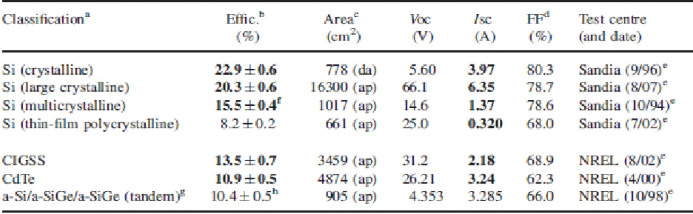
Table 1 provides a summary of the state of the art conversion efficiency reported for various semiconductors based solar cells (sources adapted from MA Green [20].
Table I. Confirmed terrestrial cell and submodule efficiencies measured under the global
AM1.5 spectrum (1000W/m2) at 25°C
a
CIGS=CuInGaSe2; a-Si=amorphous silicon/hydrogen alloy.
b
Effic.=efficiency.
c
(ap)=aperture area; (t)=total area; (da)=designated illumination area.
d
31
e
FhG-ISE=Fraunhofer Institut fu¨r Solare Energie systeme; JQA=Japan Quality Assurance; AIST=Japanese National Institute of Advanced Industrial Science and Technology.
f
Recalibrated from original measurement.
gReported on a „per cell‟ basis. h
Not measured at an external laboratory.
i
Stabilised by 800 h, 1 sun AM1.5 illumination at a cell temperature of 50°C.
j
Measured under IEC 60904-3 Ed. 1: 1989 reference spectrum.
k
Stability not investigated.
l
Stabilised by 174 h, 1 sun illumination after 20 h, 5 sun illumination at a sample temperature of 50°C.
Table II. Confirmed terrestrial module efficiencies measured under the global AM1.5
spectrum (1000 W/m2) at a cell temperature of 25°C
a
CIGS=CuInGaSe2; a-Si=amorphous silicon/hydrogen alloy.
b
Effic.=efficiency.
c
(ap)=aperture area; (t)=total area; (da)=designated illumination area.
d
FF=fill factor.
e
Recalibrated from original measurement.
h
Not measured at an external laboratory
g
Light soaked at NREL for 1000 hours at 50°C, nominally 1-sun illumination.
h
32
I.9 Technologies for the Reduction of Efficiency Losses
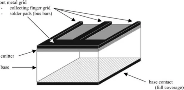
A schematic representation of part of a conventional solar cell is depicted in Figure
(I-15).
Figure I-15 Schematic representation of a conventional solar cell
The base is the main part of the mechanical structure. The emitter is located near the top or front surface. A metal grid to extract the carrier from the device, contacts each of these silicon regions. Whereas the rear surface is often fully covered (as in the drawing), on the front surface the metal grid is the result of a trade-off between having low coverage to limit optical losses and high coverage to limit resistive losses. Most manufactures apply a front grid consisting of thin parallel lines (fingers) that transport the current to centrally located bus bars. The bus bars are relatively wide and can be used as solder pads to connect to the external leads. In order to reduce the optical and electrical losses mentioned above, in this part, the optical and electrical technologies made for reducing efficiency losses will be described.
I.9.1 Technologies for the Reduction of Optical Losses (light confinement)
It is generally accepted that the cost of photovoltaic conversion has to diminish for PV to become of major importance as a renewable energy source. For crystalline silicon wafer technology, the silicon material is a major cost item. One decision to make more efficient use of the costly silicon material is the use of thinner silicon layers.
33 The current of a cell is directly related to the amount of light absorbed. One source of optical losses is that silicon (as indirect band gap material) absorbs infrared light in a rather weak way. Current wafers typically have a thickness of 300 μm. This is not enough to absorb the infrared light in one pass through the wafer. This effect becomes more important as wafers become thinner. Silicon however has a relatively large refractive index (around 3.5) [21]. This high refractive index enables the use of total internal reflection as a powerful means to make light bounce up- and down many times in the silicon wafer, enhancing the path length of rays and hence increase the chance that an infrared photon is absorbed. Thinner silicon solar cells require light-trapping methods to be used in order to maintain good absorption of infrared light and hence maintain cell current and efficiency.
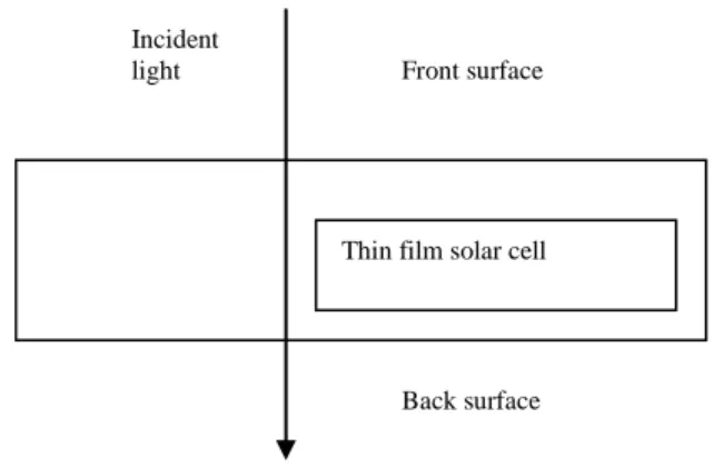
Light trapping technology is able to diffract and reflect the light inside the cell, such that the light bounces back and forth inside the cell, results in increase of optical path length. Front surface of cell is defined to be the surface where the incidence light comes. Back surface of cell is defined as the other side of front surface. Figure I-16 illustrates front and back surface.
There are three general methods to confine/ trap light inside a solar cell by using Antireflection Coating (ARC), surface texturing, and back reflector.
I.9.1.1 Antireflection Coating (ARC)
Anti-reflection coatings reduce the light loss by making use of phase changes and the dependence of the reflectivity on the refractive index. Antireflection Coating (ARC) by
Front surface
Back surface Thin film solar cell Incident
light
34 depositing a layer of material that has lower refractive index (nARC) is used to reduce the
amount of incident light that would normally be reflected ( i.e. this layer reduces the light loss) . Single layer ARC has zero reflection at its center λc wavelength when the thickness of layer is tARC=0.13 λc/nARC , where λc=576nm and nARC=1.87 [22].
There are many candidate of ARC, such as, ZnO, SiOxNy, Si3N4. ZnO, SiOxNy, and
Si3N4 can be deposited using RF sputtering [21], LPCVD [23]. Silicon nanowire can be used
as antireflection coating too. For thin film solar cell with intergitated top contacts, the function of an ARC is to reduce the reflection of incoming light, passivize the surface, and provide insulation allowing selective plating of intergitated top contacts [23].Si3N4 is chosen since it can perform all three functions well.
I.9.1.2 Surface Texturing
Surface texturing, either in combination with an anti-reflection coating or by itself, can also be used to minimise reflection. Any "roughening" of the surface reduces reflection by increasing the chances of reflected light to bounce back onto the surface, rather than out to the surrounding air. Surface texturing of front or both front and back surface of a solar cell (based on silicon for example) is used to scatter the photon such that optical path length increases. Texturization is achieved by creating a topology of small, densely packed tetrahedral grooves, V-grooves or random pyramids that act as light traps on the solar cell‟s surface. When light impinges on this textured surface, reflection occurs at such an angle that it is deflected into a new point on the surface.
Multiple interactions occur with the silicon, thus reducing the amount of light normally lost through reflection. Together with an antireflection coating the reflection of sunlight can be kept well under 3%, making the cell appear black (“black cell”). The textured surface also provides a reduction in path length to the junction which is most pronounced for longer wavelength light, thereby increasing longer wavelength collection efficiency (an important factor for thin devices). As bulk region diffusion length is reduced by the effects of radiation, the reduced effective path length enables a contoured surface device to maintain more of the lower wavelength response than a comparable smooth cell. Texturization increases solar absorbance also in the wavelength region not contributing to the carrier generation. Figure (I-16) illustrates the pyramid surface texture.
35 Figure I-16 Texturization by raised pyramids
I.9.1.3 Back Surface Reflector (BSR)
The absorption of photons from the incident sunlight depends on the absorption coefficient, which is high for short wavelengths and low for longer wavelengths. Accordingly red and infrared light penetrate deeper into the silicon material and a big portion is scattered or absorbed at the rear side contact. Polishing and coating the rear side with a thin aluminium reflector makes the back contact reflective give longer wavelengths a second chance at being absorbed and the energy which is not absorbed is re-emitted through the front surface leading to a reduction in cell absorbance.
Back reflector is used to reflect back the incident photon. Distributed back refractor (BDR) is proposed to replace current metal back refractor. The reflectivity of aluminium back reflector is typically > 95% for normal incidence and <80% for oblique incidence, while the reflectivity of distributed brag reflector is much more superior of >99.8% over a wide range of wavelength (800-1100nm) and better for oblique incidence [22]. The limitation of back reflector is that at most it can only enhance optical path length to twice of the cell thickness. To address this limitation, diffraction grating DG is used on back surface to diffract the light inside solar cell to certain angles based on different diffraction orders [23]. When only BDR is used, 70% of light was lost due to low reflection; when BDR coupled with DG are used, they complement each other such that fewer light is lost [23].
DBR consists of pair of Si and SiO3 layers in 8 stacks, and deposited using PECVD. The
DBR is deposited at temperature less than 450°C but DBR performance is stable even after
36 I.9.2 Technologies for the Reduction of Losses Due to Recombination
I.9.2.1 Recombination Mechanism in Silicon Solar Cell
In a conventional silicon solar cell, recombination can occur in five regions: • The front surface;
• The emitter region (N+
);
• The junction (the depletion region of the junction); • The base region (P);
• The back surface
Therefore, there are principally two types of recombination: the recombination mechanisms in bulk (volume) and the surface recombination.
1. Recombination Mechanisms in the Bulk of the Silicon Solar Cell
There are three fundamental recombination mechanisms in a bulk semiconductor. (a) Radiative or band-to-band recombination
(b) Auger recombination
(c) Recombination through defect or trap levels (often referred to as Shockley-Read-Hall recombination (SRH recombination))
These different processes are further illustrated with the Figure (I-17)
Figure I-17 Schematic representation of carrier recombination mechanisms in semiconductors
37
Radiative Recombination
Radiative recombination (band-to-band recombination) corresponds to the recombination process where a free electron falls directly from the conduction band and recombines with a free hole in the valence band with all or most of the excess energy dissipated in the form of a photon. The radiative volume recombination rate, UBB, is simply proportional to the electron concentration in the conduction band (the free-electron concentration) and the hole concentration in the valence band (the free-hole concentration):
Bnp
UBB (I-14)
Where: B is the coefficient of radiative recombination, n is the free-electron concentration and
p is the free-hole concentration. From detailed balance calculation, the value of B for Si was
calculated to be 2×10 -15 cm 3 s -1
[24]. At thermal equilibrium (Δn=0), UBB is equivalent to the thermal generation rate, Gth; the expression for UBB at thermal equilibrium is
2 0 0 i th BB G Bn p Bn U (I-15)
Where: n0 and p0 are the thermal equilibrium concentrations of free electrons and free holes and ni is the intrinsic carrier concentration. From Equation I-14 and I-15, the radiative recombination lifetime can readily be obtained as
n n
p n
B n BB 0 0 . . (I-16)Consequently, the expressions for the radiative recombination lifetime under low and high injection are as follows:
doped lli BB N B. 1 , and n B hli BB . 1 , (I-17)
Ndoped is the donor (ND) or the acceptor (NA) concentration for n- or p-type semiconductors, respectively. Note that the radiative recombination lifetime stays constant at low injection and decreases with injection in intermediate and high injection regimes.
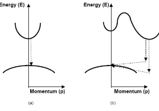
The radiative recombination in an indirect band gap semiconductor such as Si is considered to be small compared to other types of recombination. This is because the process
38 involves phonon as the fourth particle (apart from an electron, a hole, and a photon) to conserve the momentum (see Figure I-18).
Figure I-18 Schematic representation of radiative recombination for (a) direct band gap (e.g. GaAs) and (b) indirect band gap (e.g. Si).
Auger Recombination
Auger recombination is a three-particle interaction where an electron in the conduction band and a hole in the valence band recombine giving the excess energy to the third electron or hole. The eeh and ehh denote the cases where the excess energy is transferred to an electron and a hole, respectively. The Auger recombination rate, UAuger, is given by
eeh ehh Auger U U U Or 2 2 . . . .n p C np C UAuger n p (I-18)
The Cn and Cp are the Auger coefficients for electrons and holes, respectively. Consequently, the expressions for the Auger recombination lifetime under low and high injection are as follows:
39 N type Si , 2 . 1 D n lli Auger N C and ,
2 . 1 n C Cn p hli Auger (I-19) P-type Si , 2 . 1 A p lli Auger N C and ,
2 . 1 n C Cn p hli Auger (I-20)The most commonly used values for the Auger coefficients were determined by Dziewior and Schmid (Cn=2.8×10
-31 cm 6 s -1 and Cp=0.99×10 -31 cm 6 s -1
) for Si with a doping concentration greater than 5×10
18
cm
-3
[25].
The Auger recombination lifetime is, to the first order, a quadratic function of the carrier concentration, as opposed to a linear function in the case of the radiative recombination lifetime. As a result, Auger recombination dominates the lifetime at high doping or at high injection.
Shockley Read Hall Recombination (SRH)
Defects in semiconductors can create energy levels within the band gap that can greatly enhance the recombination process. These trap levels form stepping stones whereby an electron falls from the conduction band to the defect level and then from the defect level to the valence band. This type of recombination normally dominates the net recombination rate in low quality materials with a high defect density. The dynamic of the recombination process via trap levels inside the band gap was first derived by Shockley and Read and Hall (so-called SRH recombination theory) [26-27]. Important assumptions made in the derivation of the SRH recombination rate are summarized in [27] and are listed below
(a) No radiative recombination or Auger recombination involves.
(b) The semiconductor is non-degenerate.
(c) The energy level of the defects does not change with their charging properties.
(d) The relaxation time of the charge carriers caught by the defects is negligibly small compared to the average time between two emission processes.
(e) Fermi-Dirac statistic applies.
(f) The defects do not interact with each other (i.e., an electron cannot make a transition from a defect level to another).
40 The SRH volume recombination rate, USRH, for single-energy level traps is then given by:
1
0
1
0 2 p p n n n np U n p i SRH (I-21)The τn0 and τp0 are the characteristic electron and hole lifetimes, which are related to the thermal velocity of the charge carrier, υth, the defect concentration, Nt, and the capture cross-sections of electron and hole of the specific defect, σn and σp as
t th n n N 0 1 And t th p p N 0 1 (I-22) KT E E n n1 iexp t i And KT E E n p1 iexp i t (I-23)
By definition, n1 and p1 are the free-electron and the free-hole concentrations in the case in which the Fermi level (EF) lies at the trap energy level (Et). The SRH recombination lifetime can then be obtained as follows:
n p n p p n n n p SRH 0 0 1 0 1 0 (I-24)Consequently, the expressions for the SRH recombination lifetime under low and high injection are as follows:
N-type Si
D n p lli SRH N p n 1 0 0 , and SRH,hli n0 p0 (I-25)
P-type Si
A p n lli SRH N n n 1 0 0 , and SRH,hli n0 p0 (I-26)
For traps located at the middle of the band gap (Et≅Ei), both n1 and p1 become small and equal to ni Consequently, the SRH lifetime under low injection can further be simplified as:
N-type Si SRH,lli p0 for mid-gap traps (I-27) P-type Si SRH,lli n0 for mid gap traps. (I-28)
41 As can be seen from Equation I-24 through I-25, with respect to the location of the traps in the band gap, the SRH lifetime becomes lowest when the traps lie at the middle of the band gap. Consequently, the mid-gap traps are considered to be the most damaging traps that can greatly enhance the overall recombination in the device.
In reality, all three recombination processes discussed above take place at the same time. The net volume recombination can be obtained simply by adding the three recombination rates as follows: SRH Auger BB net U U U U (I-29)
The net lifetime can therefore, be obtained as:
SRH Auger BB net 1 1 1 1 (I-30) 2. Surface Recombination
Surface recombination corresponds to a phenomenon where excited electrons in the conduction band recombine with holes in the valence band via defect levels at the surface, called surface states (Figure I-19). These surface states are the result of the abrupt discontinuity of a crystalline phase at the surface, which forms unsatisfied dangling Si bonds. The recombination via these surface states can be explained through minor modification of the volume SRH recombination theory.
42 It is useful to first introduce two main quantities that are used to quantify the surface recombination activity:
(a) Surface recombination rate, Us (cm
-2
s
-1
): A recombination rate of carriers per unit area per
unit time
(b) Surface recombination velocity, S or SRV (cm/s): A velocity of the excited carrier flowing to a surface.
These parameters are related to the surface recombination rate by the following equation:
n Us S
(I-31)
With minor modifications to the expression of the volume SRH recombination (Equation I-21), the surface recombination rate, Us, for single-energy level surface states can be obtained as 0 1 0 1 2 . n s p s i s s s S p p S n n n p n U (I-32)
Where ns and ps are the electron and the hole volume concentrations at the surface and Sn0 and
Sp0 are the characteristic surface recombination velocities of the surface states, which are related the surface states density, Nst (cm
-2 ) as: st th p p N S 0 . . and Sn0 n.th.Nst (I-33)
Consequently, through the definition of the surface recombination velocity (Equation I-31), the SRH surface recombination velocity can be obtained as
0 1 0 1 0 0 n s p s s s S p p S n n n P n S (I-34)
In reality, surface states are not localized at a single-energy level but are distributed across the band gap of a semiconductor. Here, the total surface recombination rate is obtained by integrating Equation I-31 through the entire band gap of a semiconductor:
![Table 1 provides a summary of the state of the art conversion efficiency reported for various semiconductors based solar cells (sources adapted from MA Green [20]](https://thumb-eu.123doks.com/thumbv2/123doknet/3467129.101295/31.892.166.844.318.972/provides-summary-conversion-efficiency-reported-semiconductors-sources-adapted.webp)