HAL Id: tel-03209228
https://hal.archives-ouvertes.fr/tel-03209228
Submitted on 27 Apr 2021HAL is a multi-disciplinary open access archive for the deposit and dissemination of sci-entific research documents, whether they are pub-lished or not. The documents may come from teaching and research institutions in France or abroad, or from public or private research centers.
L’archive ouverte pluridisciplinaire HAL, est destinée au dépôt et à la diffusion de documents scientifiques de niveau recherche, publiés ou non, émanant des établissements d’enseignement et de recherche français ou étrangers, des laboratoires publics ou privés.
bandgap semiconducting nanoparticles of ZnO for
application as white light emitting diodes
Yu Zhang
To cite this version:
Yu Zhang. Fabrication, structural and spectroscopic studies of wide bandgap semiconducting nanopar-ticles of ZnO for application as white light emitting diodes. Material chemistry. Université de Lyon, 2020. English. �tel-03209228�
N°d’ordre NNT : 2020LYSEI046
THESE de DOCTORAT DE L’UNIVERSITE DE LYON
opérée au sein de
l’INSA de Lyon
Ecole Doctorale
N° 34
MATÉRIAUX DE LYON
Spécialité/ discipline de doctorat
:Matériaux
Soutenue publiquement le 30/06/2020, par :
Yu Zhang
Fabrication, structural and spectroscopic studies
of wide bandgap semiconducting nanoparticles of
ZnO for application as white light emitting diodes
Devant le jury composé de :
Nom, prénom grade/qualité établissement/entreprise Président.e (à préciser après la soutenance)
Chadeyron, Geneviève Professeure ICCF- Sigma Clermont Rapporteure
Charra, Fabrice Directeur de Recherche IRAMIS-CEA Rapporteur
Andraud, Chantal Directrice de Recherche CNRS, LC-ENS Lyon Examinatrice
Rinnert, Hervé Professeur IJL-Univ. Lorraine Examinateur
Masenelli, Bruno Professeur, INL-INSA Lyon Directeur de thèse Apostoluk, Alexandra Maitresse de conférence, INL-INSA Lyon Co-directrice de thèse
Danièle, Stéphane Professeur, C2P2-UCBL1 Invité
Département FEDORA – INSA Lyon - Ecoles Doctorales – Quinquennal 2016-2020
SIGLE ECOLE DOCTORALE NOM ET COORDONNEES DU RESPONSABLE
CHIMIE CHIMIE DE LYON
http://www.edchimie-lyon.fr Sec. : Renée EL MELHEM Bât. Blaise PASCAL, 3e étage [email protected] INSA : R. GOURDON
M. Stéphane DANIELE
Institut de recherches sur la catalyse et l’environnement de Lyon IRCELYON-UMR 5256
Équipe CDFA
2 Avenue Albert EINSTEIN 69 626 Villeurbanne CEDEX [email protected]
E.E.A. ÉLECTRONIQUE, ÉLECTROTECHNIQUE,
AUTOMATIQUE http://edeea.ec-lyon.fr
Sec. : M.C. HAVGOUDOUKIAN
M. Gérard SCORLETTI
École Centrale de Lyon
36 Avenue Guy DE COLLONGUE 69 134 Écully
Tél : 04.72.18.60.97 Fax 04.78.43.37.17
E2M2 ÉVOLUTION, ÉCOSYSTÈME,
MICROBIOLOGIE, MODÉLISATION http://e2m2.universite-lyon.fr
Sec. : Sylvie ROBERJOT Bât. Atrium, UCB Lyon 1 Tél : 04.72.44.83.62 INSA : H. CHARLES
M. Philippe NORMAND
UMR 5557 Lab. d’Ecologie Microbienne Université Claude Bernard Lyon 1 Bâtiment Mendel
43, boulevard du 11 Novembre 1918 69 622 Villeurbanne CEDEX
EDISS INTERDISCIPLINAIRE SCIENCES-SANTÉ
http://www.ediss-lyon.fr Sec. : Sylvie ROBERJOT Bât. Atrium, UCB Lyon 1 Tél : 04.72.44.83.62 INSA : M. LAGARDE
Mme Sylvie RICARD-BLUM
Institut de Chimie et Biochimie Moléculaires et Supramoléculaires (ICBMS) - UMR 5246 CNRS - Université Lyon 1
Bâtiment Curien - 3ème étage Nord 43 Boulevard du 11 novembre 1918 69622 Villeurbanne Cedex Tel :
+33(0)4 72 44 82 32
INFOMATHS INFORMATIQUE ET MATHÉMATIQUES
http://edinfomaths.universite-lyon.fr Sec. : Renée EL MELHEM
Bât. Blaise PASCAL, 3e étage
Tél : 04.72.43.80.46
M. Hamamache KHEDDOUCI
Bât. Nautibus
43, Boulevard du 11 novembre 1918 69 622 Villeurbanne Cedex France Tel : 04.72.44.83.69
Matériaux MATÉRIAUX DE LYON
http://ed34.universite-lyon.fr Sec. : Stéphanie CAUVIN Tél : 04.72.43.71.70 Bât. Direction [email protected] M. Jean-Yves BUFFIÈRE INSA de Lyon MATEIS - Bât. Saint-Exupéry 7 Avenue Jean CAPELLE 69 621 Villeurbanne CEDEX
Tél : 04.72.43.71.70 Fax : 04.72.43.85.28
MEGA MÉCANIQUE, ÉNERGÉTIQUE,
GÉNIE CIVIL, ACOUSTIQUE http://edmega.universite-lyon.fr Sec. : Stéphanie CAUVIN Tél : 04.72.43.71.70 Bât. Direction [email protected]
M. Jocelyn BONJOUR INSA
de Lyon
Laboratoire CETHIL Bâtiment Sadi-Carnot 9, rue de la Physique
69 621 Villeurbanne CEDEX
ScSo
ScSo*
http://ed483.univ-lyon2.fr Sec. : Véronique GUICHARD INSA : J.Y. TOUSSAINT Tél : 04.78.69.72.76
M. Christian MONTES
Université Lyon 2 86 Rue Pasteur
69 365 Lyon CEDEX 07
Acknowledgement
This thesis was accomplished under the direction of my two supervisors, Bruno Masenelli and Aleksandra Apostoluk, who helped me in so many ways throughout the PhD years, from resolving scientific issues, to planning personal career, and to adapting to local environment. It was reassuring to have two mentors to whom I could always turn for help when needed. They always encouraged me to become an independent researcher and gave me invaluable advice without reservation on how to achieve it. The lessons I learnt from them not only assisted me in conquering the biggest challenge in my life, but will also benefit me in the long term, both professionally and personally. I am forever grateful for their guidance.
The projects in the thesis would not have been possible without our collaborators, the team of Stéphane Daniele from C2P2, IRCELYON, and Lotus Synthesis SAS. The preparation of the materials is attributed to Nicolas Le Bail, Thibaut Cornier, Christophe Theron, and Timoté Gard. The expertise of the team in the chemical processes is valuable and their cooperation in the design of the materials is highly appreciated.
My heartfelt appreciation also goes to those who provided their assistance in certain characterizations and analyses. I would like to thank Karine Masenelli-Varlot for her expertise in TEM and Bruno Canut for his expertise in RBS. Jean-Marie Bluet helped me with several characterizations, including FTIR and PLE measurements. Fabien Mandorlo shared his knowledge in CIE color space and calculated the positions of the spectra of our samples in UCS diagrams. Sandrine Cardinal provided technical and scientific assistance in the acquisition of XRD spectra. I learnt a great deal from each of them and I am grateful for their kind help and shared knowledge.
We are indebted to the team of Christophe Dujardin from iLM for their contribution in the characterization of thermal stability. In particular, I wish to thank Gilles Ledoux for his thorough guidance in the experiments.
The thesis program was supported by the cooperation between INSA Lyon and China Scholarship Council. My sincerest gratitude is obliged to both establishments, for providing me with the opportunity to join the excellent team at Institute of Nanotechnology of Lyon (INL). The scientific platform provided by INL is deeply appreciated and I am grateful for the administration team and the technical staff as they made my time at the laboratory easy and enjoyable.
I would like to express my thanks to the colleagues at INL whom I have the honor to call my friends, Ali Jaffal, Nicolas Gaignebet, Florian Berry, Benoit Guillo-Lohan, Nelly Moulin, Xiao Li, Benjamin Fornacciari, Solène Brottet, Alexander Singaevsky, and Sofia Rodichkina, for sharing some of the most memorable moments in my PhD years. It has been a great pleasure to work and discuss with them. I
would also like to acknowledge many other friends, for their support and encouragement, especially the PhD holders, for sharing their personal experience and wisdom.
I
Fabrication, études structurales et spectroscopiques de nanoparticules semi-conductrices à large bande interdite de ZnO pour application en diodes électroluminescentes blanches
Résumé
L’industrie de l'éclairage est actuellement dominée par les luminophores à base de terres rares. Une utilisation à si grande échelle d’éléments de terres rares est à l’origine de problèmes environnementaux et contribue au changement climatique. Grâce à ses défauts intrinsèques, ZnO a été considéré comme un luminophore potentiellement exempt de terres rares pour les diodes électroluminescentes blanches (WLEDs). L'objectif de cette thèse est de développer un matériau électroluminescent blanc efficace et stable à base de nanoparticules de ZnO. Un système nanohybride de nanoparticules de ZnO incorporées dans des mésosphères d'acide polyacrylique (PAA) a été développé par voie d'hydrolyse. Trois défis doivent être relevés pour que le système nanohybride ZnO / PAA soit applicable aux WLEDs. La première consiste à régler la couleur, ou la chaleur, d'émission du système, pour répondre aux exigences spécifiques des WLEDs; la deuxième est d'améliorer le rendement quantique de photoluminescence (PL QY); la dernière consiste à améliorer la stabilité thermique du système, car les WLEDs fonctionnent généralement au-dessus de la température ambiante. Deux études sont menées pour aborder ces questions.
Dans la première étude, le dopage par des éléments autres que des terres non rares est employé pour régler la couleur d'émission de ZnO. L'objectif est d'acquérir une compréhension générale de l'effet du dopage sur les propriétés structurales et optiques du nanohybride ZnO / PAA. Une série de dopants métalliques de nature, taille, valence et concentration différentes sont introduits indépendamment dans le système nanohybride au cours du processus d'hydrolyse. On constate que la présence de dopant a un impact sur la structure mésosphérique. Des concentrations de dopage élevées peuvent rendre les mésosphères plus grosses et les gros ions peuvent même inhiber la formation des mésosphères. La taille des cristaux de ZnO est également affectée par le dopage. Les nanohybrides dopés présentent une large émission visible, avec un décalage vers le rouge du pic d'émission de 2,47 eV de ZnO non dopé jusqu'à 2,08 eV. Le décalage dépend de la nature, de la valence et de la concentration du dopant. Le PL QY est généralement réduit par le dopage, quel que soit le dopant. Cependant, il peut être maintenu ou même amélioré en dopant avec de petits ions à une faible concentration de dopage (0,1 at%). La couleur d'émission du ZnO dopé peut être réglée entre 2,47 eV et 2,17 eV sans dégrader PL QY.
Dans la deuxième étude, un revêtement de silice est adopté pour améliorer le PL QY et la stabilité thermique du nanohybride ZnO / PAA. Différents précurseurs de ZnO / PAA sont enrobés de silice par l’hydrolyse d'orthosilicate de tétraéthyle (TEOS) en présence d'ammoniac (NH4OH). Les quantités de TEOS et de NH4OH sont deux facteurs corrélés qui déterminent l'intégrité des mésosphères de PAA et
II
l'épaisseur du revêtement de silice. Les effets de la dose de TEOS et de la concentration d’ammoniac sont étudiés indépendamment. La structure cristallographique des nanocristaux de ZnO n'est pas modifiée par le revêtement de silice, qui est incorporé sous forme de phase amorphe. Le PL QY est aisément amélioré par un revêtement de silice dans la plupart des cas, avec une amélioration optimale du PL QY de 619 % par rapport à celle du précurseur ZnO / PAA. Un modèle de structure est établi pour expliquer l'évolution des mésosphères au cours du processus de revêtement. Le cœur du modèle est l'amination des groupes COOH dans les chaînes de PAA, qui dégrade les mésosphères. L'amélioration optimale de PL QY est obtenue lorsque les mésosphères sont conservées par une quantité appropriée d'ammoniac et sont renforcées par un revêtement de silice d'une épaisseur appropriée. Enfin, la stabilité thermique du ZnO / PAA dopé au métal ou revêtu de silice est examinée de la température ambiante à 100 ° C. Pour les deux matériaux, l'intensité de l'émission visible diminue à mesure que la température augmente. Le revêtement de silice réduit l'impact de la chaleur sur le matériau en améliorant considérablement le PL QY. Le problème est atténué dans une certaine mesure mais pas complétement éliminé.
III
Abstract
The lighting industry is currently dominated by earth-based phosphors. Such large-scale use of rare-earth elements is causing environmental issues and contributing to the climate change. Owing to its intrinsic defects, ZnO has been considered a potential rare-earth-free phosphor for white light-emitting diodes (WLEDs). The objective of the thesis is to develop an efficient and stable white light-emitting material based on ZnO nanoparticles. A nanohybrid system comprising mainly ZnO nanocrystals embedded in polyacrylic acid (PAA) mesospheres has been developed via hydrolysis route. Three challenges are to be met for the ZnO/PAA nanohybrid system to be applicable in WLEDs. The first is to tune the emission color, or warmth, of the system, to meet specific requirements of WLEDs; the second is to improve the photoluminescence quantum yield (PL QY); the last is to enhance the thermal stability of the system, for WLEDs usually operate above room temperature. Two studies are carried out to undertake the above issues.
In the first study, doping of non-rare-earth elements is employed to tune the emission color of ZnO. The aim is to gain a general understanding of the effect of doping on the structural and optical properties of the ZnO/PAA nanohybrid. A series of metal dopants of different nature, size, valence, and concentration are independently introduced into the nanohybrid system during the hydrolysis process. It is found that the presence of dopant has an impact on the mesospheric structure. High doping concentrations may render bigger mesospheres and large ions can even inhibit the formation of the mesospheres. The crystal size of ZnO is also affected by doping. The doped nanohybrids exhibit a broad visible emission, with a redshift of emission peak from 2.47 eV of undoped ZnO to as far as 2.08 eV. The redshift is dependent on the nature, valence, and concentration of the dopant. The PL QY is generally reduced by doping, regardless of the dopant. However, it can be maintained or even improved by doping small ions at a low doping concentration (0.1 at%). The emission color of doped ZnO can be tuned between 2.47 eV and 2.17 eV without degrading PL QY.
In the second study, silica coating is adopted to improve the PL QY and the thermal stability of ZnO/PAA nanohybrid. Different ZnO/PAA precursors are coated by silica via hydrolysis of tetraethyl orthosilicate (TEOS) under the presence of ammonia (NH4OH). The amounts of TEOS and NH4OH are two correlated factors that determine the integrity of the PAA mesospheres and the thickness of silica coating. The effects of TEOS loading and ammonia concentration are investigated independently. The crystallographic structure of ZnO nanocrystals is not modified by silica coating, which is incorporated as an amorphous phase. The PL QY is readily improved by silica coating in most cases, with an optimal PL QY improvement by 619 % from that of ZnO/PAA precursor. A structure model is established to explain the evolution of mesospheres during the coating process. The core of the model is the amination of COOH groups in PAA chains, which degrades the mesospheres. The optimal PL QY improvement is
IV
achieved when the mesospheres are preserved under an appropriate amount of ammonia and are strengthened by silica coating with an appropriate thickness.
Finally, the thermal stability of both metal-doped and silica-coated ZnO/PAA is examined from room temperature to 100 °C. For both materials, the intensity of the visible emission decreases as the temperature increases. Silica coating reduces the impact of heat on the material by drastically improving the PL QY. The issue is alleviated to some extent but not completely eliminated.
i
Contents
Résumé
... IAbstract
... IIIList of Acronyms and Abbreviations
... vList of Figures
... viiChapter 1 State-of-the-Art
... 1Context ... 1
1.1 White light-emitting diodes (WLEDs) ... 1
1.1.1 WLEDs criteria ... 2
1.1.1.1 Quantum efficiency ... 2
1.1.1.2 Correlated color temperature ... 3
1.1.1.3 Color rendering index ... 3
1.1.1.4 Other criteria ... 5
1.1.2 UV-excited phosphors ... 5
1.1.3 Blue-excited phosphors ... 6
1.1.4 ZnO as RE-free phosphor ... 8
1.2 Undoped ZnO ... 9
1.2.1 Photoluminescence of undoped ZnO ... 9
1.2.2 UV emission ... 11 1.2.3 Visible emission ... 14 1.3 Doping of ZnO ... 17 1.3.1 Rare-earth doping ... 17 1.3.2 Non-rare-earth doping ... 21 1.3.3 Summary on doping ... 25 1.4 ZnO nanostructures ... 26
Chapter 2 Materials and Characterizations
... 29ii
2.1.1 Hydrolysis of ZnEt2 ... 29
2.1.2 Metal-doped ZnO nanohybrids ... 30
2.1.3 Silica-coated ZnO nanohybrids ... 32
2.2 Structural characterizations ... 33
2.2.1 X-Ray Diffraction ... 34
2.2.2 Transmission Electron Microscopy ... 36
2.2.3 Rutherford Backscattering Spectrometry ... 38
2.2.4 Fourier Transform Infrared spectroscopy ... 39
2.3 Optical characterizations ... 41
2.3.1 Photoluminescence spectroscopy ... 41
2.3.2 Photoluminescence Excitation spectroscopy ... 42
2.3.3 Measurement and calculation of photoluminescence quantum yield ... 43
2.3.4 Photoluminescence at high temperature ... 47
Chapter 3 Metal-Doped ZnO Nanohybrids
... 493.1 Microstructure of metal-doped ZnO nanohybrids ... 49
3.1.1 Morphology ... 49
3.1.2 Crystal structure indexing ... 52
3.1.3 Presence of PAA... 54
3.1.4 Presence of dopants ... 55
3.1.5 Effect of dopant on the microstructure ... 57
3.1.5.1 Mesosphere structure ... 57
3.1.5.2 Crystal structure... 58
3.1.5.3 Crystal size ... 61
3.1.5.4 Summary ... 62
3.2 Optical properties of metal-doped ZnO nanohybrids ... 62
3.2.1 Photoluminescence ... 62
3.2.1.1 Effect of dopant type ... 63
iii
3.2.1.3 Effect of valence ... 64
3.2.1.4 Summary ... 67
3.2.2 Photoluminescence quantum yield ... 68
3.2.3 Photoluminescence excitation ... 69
3.2.4 Role of dopant ... 70
3.2.4.1 Dopants during hydrolysis synthesis ... 70
3.2.4.2 Dopants in the nanohybrid ... 72
3.2.5 Photoluminescence at high temperature ... 74
3.3 Conclusion ... 75
Chapter 4 Silica-Coated ZnO Nanohybrids
... 774.1 Instability of ZnO/PAA precursors ... 77
4.2 Effect of TEOS ratio ... 81
4.2.1 Microstructure ... 81
4.2.1.1 X-ray diffraction ... 81
4.2.1.2 Transmission electron microscopy ... 83
4.2.1.3 Fourier transform infrared spectroscopy ... 84
4.2.1.4 Summary ... 85
4.2.2 Optical properties ... 86
4.2.2.1 Photoluminescence ... 86
4.2.2.2 Photoluminescence quantum yield ... 86
4.3 Effect of ammonia content ... 87
4.3.1 Microstructure ... 88
4.3.1.1 X-ray diffraction ... 88
4.3.1.2 Transmission electron microscopy ... 89
4.3.1.3 Rutherford backscattering spectrometry ... 92
4.3.1.4 Structure model ... 93
4.3.2 Optical properties ... 94
iv
4.3.2.2 Photoluminescence quantum yield ... 96
4.3.2.3 Photoluminescence excitation ... 97
4.3.3 Thermal stability ... 98
4.4 Role of silica coating ... 101
4.5 Conclusion ... 102
General Conclusions
... 105References
... 107Appendix I
XRD spectra of metal-doped ZnO nanohybrids ... 121Appendix II
HRTEM images of metal-doped ZnO nanohybrids ... 124Appendix III
FTIR spectra of metal-doped ZnO nanohybrids ... 126Appendix IV
RBS spectra of metal-doped ZnO nanohybrids ... 131Appendix V
PL spectra of metal-doped ZnO nanohybrids ... 133Appendix VI
EDX spectrum of silica-coated ZnO/PAA nanohybrid (3.8Si-1A) ... 138v
List of Acronyms and Abbreviations
BBE Band to Band Emission
CB Conduction Band
CCD Charge-Coupled Device
CCT Correlated Color Temperature
CIE Commission Internationale de l'Éclairage
CRI Color Rendering Index
DAP Donor-Acceptor Pairs
DLE Deep Level Emission
EDS, EDX Energy Dispersive X-Ray Spectroscopy
EQE External Quantum Efficiency
FFT Fast Fourier Transform
FTIR Fourier Transform Infrared Spectroscopy HAADF High Angle Annular Dark-Field
HRTEM High-Resolution Transmission Electron Microscopy
IQE Internal Quantum Efficiency
IR Infrared
LED Light-Emitting Diode
MBE Molecular Beam Epitaxy
NBE Near Band Edge Emission
Oi Oxygen Interstitial
OZn Oxygen Anti-Site
PAA Polyacrylic Acid
PAAH Protonated Polyacrylic Acid
vi
PLE Photoluminescence Excitation
QE Quantum Efficiency
RBS Rutherford Backscattering Spectrometry
RE Rare Earth
REE Rare Earth Elements
RGB Red, Green and Blue
RT Room Temperature
STEM Scanning Transmission Electron Microscopy
TEM Transmission Electron Microscopy, Transmission Electron Microscope TEOS Tetraethyl Orthosilicate
TM Transition Metal
UV Ultraviolet
VB Valence Band
VO Oxygen Vacancy
VOZni Oxygen Vacancy Zinc Interstitial Defect Complex
VZn Zinc Vacancy
WLED White Light-Emitting Diode
XPS X-ray Photoelectron Spectroscopy
XRD X-Ray Diffraction
YAG:Ce Cerium-doped Yttrium Aluminum Garnet
PL Photoluminescence
PL QY Photoluminescence Quantum Yield
ZnEt2 Diethyl Zinc
ZnO Zinc Anti-Site
Zni Zinc Interstitial
vii
List of Figures
Figure 1.1 Three approaches to generate white light with LEDs: (a) with single RGB LEDs, (b) with full conversion of UV LED, and (c) with partial conversion of blue LED. [7] ... 2 Figure 1.2 (a) Commission Internationale de l'Éclairage (CIE, 1931) diagram with a black-body radiation curve (black solid line) and CCT values. (b) Luminescence spectrum of YAG:Ce and human eye sensitivity curve in grey-shaded spectrum. [7] ... 4 Figure 1.3 PL spectra of Ba2Ca(B3O6)2:0.04Eu2+, yMn2+ phosphors (λex = 330 nm). Inset shows the dependence of the energy transfer efficiency ηT on the Mn2+ content (y). [18] ... 6 Figure 1.4 PL excitation and PL emission spectra of 2 mol% Ce-doped YAG (λem = 532 nm, λex = 470 nm). [29] ... 7 Figure 1.5 (a) Wurtzite crystal structure of ZnO with indicated lattice parameters a and c. (b) Calculated band structure of ZnO. The energy of the valence band maximum was set to zero. [55] ... 9 Figure 1.6 Photoluminescent processes in ZnO. ... 10 Figure 1.7 PL spectra from ZnO epilayer obtained at (a) low temperature and (b) room temperature. The inset in (a) displays the details of the PL spectrum at near band edge (NBE) region. [65] ... 12 Figure 1.8 Normalized PL spectra of ZnO thin films for various excitation intensities at (a) room temperature and at (b) 550 K. [60] ... 13 Figure 1.9 Thermodynamic transition levels for defects in ZnO. [78] ... 14 Figure 1.10 Transition levels (measured with respect to the edge of the conduction band) of defects in ZnO reported in literature by different groups. (a) Ref [83]. (b) Ref [84]. (c) Ref [85]. (d) Ref [86]. (e) Ref [87]. (f) Ref [78]. (g) Ref [88], [89]. ... 15 Figure 1.11 Schematic diagram for the mechanism of visible emission from Ce-doped ZnO. [105] .. 18 Figure 1.12 XRD patterns of Ce-doped ZnO nanoparticles. [110] ... 19 Figure 1.13 (a) PL spectra of undoped ZnO and Ce-doped ZnO. The inset shows a schematic diagram of Ce3+ electronic levels in ZnO bandgap. (b) Normalized PL spectra in the visible range of undoped and Ce-doped ZnO. ... 20 Figure 1.14 Schematic of the energy level diagram of Cu-doped ZnO system. [131] ... 22
viii
Figure 1.15 Various morphologies of ZnO nanostructures: (a) and (b) tetrapod structures; (c) variable diameter structures; (d) nanosheets; (e) nanoshells; (f) multipods; (g), (h), and (i) nanorods.
[120] ... 26
Figure 1.16 Illustration of the mechanism on the origin of the visible emission in ZnO nanocrystal. . 27
Figure 2.1 Mesospheres of ZnO nanocrystals embedded in PAA matrix. The inset permits to notice small nanocrystals of ZnO, smaller than 10 nm. [187] ... 29
Figure 2.2 PL spectrum of ZnO nanohybrid obtained in previous study. [187] ... 30
Figure 2.3 XRD setup for the study of polycrystalline materials. ... 34
Figure 2.4 X-ray scattering from crystalline planes. ... 35
Figure 2.5 Theoretical diffraction lines of polycrystalline wurtzite ZnO. ... 35
Figure 2.6 Schemes of imaging mode (left) and diffraction mode (right) of TEM. ... 37
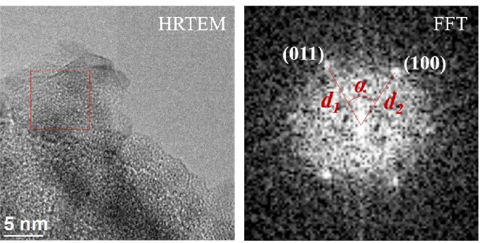
Figure 2.7 Structure indexing via fast Fourier transform (FFT) in HRTEM image. ... 37
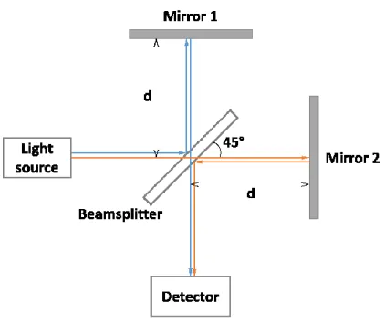
Figure 2.8 Schematic of a Michelson interferometer. ... 40
Figure 2.9 Exemplary IR spectrum of bulk ZnO. The transmittance is normalized between 0 and 1. [193] ... 40
Figure 2.10 PL spectroscopy experimental setup ... 42
Figure 2.11 Typical PLE spectrum (in blue) of ZnO along with its PL spectrum (in green). λem = 577 nm, λex = 266 nm. [195] ... 43
Figure 2.12 Illustration of three configurations with an integrating sphere for PL QY measurement. (a) The sample is not present in the sphere. (b) The sample is present but the laser is not directed onto the sample. (c) The sample is present and the laser in directed onto the sample. ... 44
Figure 2.13 Schematic of the setup for PL QY measurements. ... 45
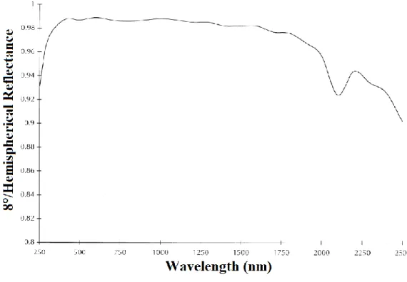
Figure 2.14 Reflectance spectrum of Spectralon coating material of the integrating sphere. ... 45
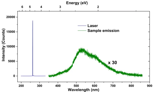
Figure 2.15 Typical laser profile and emission profile from measurement (c) for ZnO nanohybrids. The emission profile is enlarged 30 times. ... 46
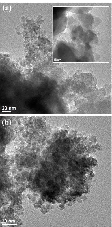
Figure 3.1 Morphologies of (a) 0.1 % Mn-doped ZnO nanohybrid and (b) 5 % Mn-doped ZnO nanohybrid. ... 50
Figure 3.2 Morphologies of ZnO nanohybrids doped with different elements at 0.1 %. (a) Cu(II) doping. (b) Bi doping. ... 51
Figure 3.3 XRD spectra of Co-doped ZnO nanohybrids at 0.1 %, 1 % and 5 % doping concentrations. ... 52
ix
Figure 3.4 HRTEM images of (a) 0.1 % Mn, (b) 5 % Mn, (c) 0.1 % Cu(II) and (d) 0.1 % Bi doping, showing nanocrystals of ZnO. The insets are FFT images of each HRTEM image, indexed to wurtzite ZnO polycrystalline structure, respectively. More HRTEM images of these samples
can be found in Appendix II. ... 53
Figure 3.5 FTIR spectra of Co-doped ZnO nanohybrids at 0.1 %, 1 % and 5 % doping. ... 54
Figure 3.6 RBS spectrum of 5 % Mn-doped ZnO nanohybrid with simulated curve (red curve) and contribution of each element (other colored curves). The inset shows contribution from Mn in detail. ... 56
Figure 3.7 EDX spectrum of 5 % Mn-doped ZnO nanohybrid. ... 57
Figure 3.8 XRD spectra of Bi-doped ZnO nanohybrids. ... 59
Figure 3.9 XRD spectra of Ag-doped ZnO nanohybrids. ... 59
Figure 3.10 XRD spectra of Ag-doped ZnO nanohybrids after calcination at 400 °C for 4 hours. ... 60
Figure 3.11 Diffraction domain size of doped ZnO nanonhybrids estimated by Scherrer equation in function of dopants and doping concentration. The dopants are arranged in the ascending order of the ionic radius. ... 61
Figure 3.12 Normalized PL spectra of Co-, Fe(III)-, Mn- and Cu(II)-doped ZnO nanohybrids at 0.1 % doping concentration in comparison with the PL spectrum of undoped ZnO nanohybrid. ... 63
Figure 3.13 PL spectra of undoped ZnO nanohybrid and Fe(II)-, Fe(III)-, Cu(I)-, and Mn-doped ZnO nanohybrids at (a) 0.1 %, (b) 1 %, and (c) 5 % doping concentrations. ... 65
Figure 3.14 PL spectra of Cu-doped ZnO nanohybrids with two different Cu valences (+1 and +2) at (a) 0.1 %, (b) 1 %, and (c) 5 % doping concentrations. ... 66
Figure 3.15 PL spectra peak position of the doped-ZnO nanohybrids in energy (eV) and wavelength (nm). The horizontal dashed line indicates the peak position of undoped ZnO nanohybrid. ... 67
Figure 3.16 PL QY of doped ZnO nanohybrids normalized to the PL QY of undoped ZnO nanohybrid. ... 68
Figure 3.17 PLE spectra of Cu(II)-doped ZnO nanohybrids at three doping concentrations. ... 70
Figure 3.18 Role of dopant during hydrolysis synthesis and in the nanohybrid composite ... 71
Figure 3.19 Position of the spectra of selected doped samples in the gamut chart in Judd’s UCS diagram (figure produced by Fabien Mandorlo)... 73
Figure 3.20 PL spectra of 0.1 % Fe(III) doped ZnO nanohybrid obtained at various temperatures from room temperature (RT) to 100 °C. ... 74
x
Figure 4.1 Normalized PL spectra of ZnO/PAA synthesized in two different batches. ... 78 Figure 4.2 Absolute PL QY values of 14 samples of ZnO/PAA precursor. The 15th uncoated sample was obtained in the same manner as the silica-coated samples but without any TEOS coating and is used as a reference. The red dashed lines indicate a PL QY window between 9 % and 19 %. ... 79 Figure 4.3 Distribution of PL QY of 15 uncoated ZnO/PAA samples. ... 79 Figure 4.4 XRD spectra of xSi-1A (x = 2, 3 and 10) ZnO nanohybrids (a) before calcination and (b) after calcination at 400 °C for 4 h... 82 Figure 4.5 TEM images of xSi-1A ZnO nanohybrids. (a) TEM and HAADF image (inset) of 3.8Si-1A. (b) HRTEM image of 3.8Si-1A with the inset showing fast Fourier transformed (FFT) image of the red square area. (c) HRTEM of 1.1Si-1A. (d) HRTEM of 10Si-1A. ... 83 Figure 4.6 FTIR spectra of ZnO/PAA and 3.8Si-1A nanohybrids. ... 85 Figure 4.7 Normalized PL spectra of silica-coated ZnO/PAA with different amount of TEOS loading.
... 86 Figure 4.8 PL QY improvement of xSi-1A samples in function of TEOS:ZnO ratio. ... 87 Figure 4.9 XRD spectra of 3.8Si-yA (y = 1, 2 and 4) ZnO/PAA nanohybrids. ... 88 Figure 4.10 Diffraction domain size of ZnO (squares) and the unassigned phase (diamonds) of three silica-coated samples (3.8Si-yA (y = 1, 2, and 4)) in function of the amount of NH4OH in solution A. The size of the unassigned phase is estimated by Scherrer equation from the peak at 2θ = 33.4°. ... 89 Figure 4.11 TEM images of 3.8Si-yA silica-coated ZnO nanohybrids. (a) and (b) 3.8Si-1A; (c) and (d) 3.8Si-2A; (e) and (f) 3.8Si-4A. ... 91 Figure 4.12 RBS spectra of 3.8Si-yA (y = 1, 2, and 4) samples. ... 92 Figure 4.13 Atomic ratio of Si to Zn in 3.8Si-yA samples calculated by RBS. ... 92 Figure 4.14 Structure model of silica-coated ZnO/PAA nanohybrids under different concentrations of NH4OH in solution A. ... 93 Figure 4.15 Normalized PL spectra of (a) 3.8Si-1A, (b) 3.8Si-2A, and (c) 3.8 Si-3A, with the spectrum of their respective uncoated ZnO/PAA precursor as the reference. ... 95 Figure 4.16 PL QY improvement of 3.8Si-yA silica-coated ZnO nanohybrids compared to their respective uncoated ZnO/PAA precursor in function of the ratio of NH4OH y in solution A. . 96 Figure 4.17 PLE spectra at λem = 550 nm of ZnO/PAA precursor and 3.8Si-yA (y = 1 and 2) samples. The spectra are normalized to the intensity at λex = 266 nm. ... 97
xi
Figure 4.18 PL spectra of (a) ZnO/PAA, (b) 3.8Si-1A and (c) 3.8Si-2A at different temperatures from 25 °C to 100 °C. ... 99 Figure 4.19 Evolution of (a) maximum PL intensity and (b) retention of maximum PL intensity relative to the initial maximum at different temperatures up to 100 °C of uncoated ZnO/PAA, 3.8Si-1A, and 3.8Si-2A. The three points standing alone at 25 °C in (b) represent the retentions of maximum PL intensity after cooling down. ... 100
1
Chapter 1 State-of-the-Art
Context
The world today is faced with increasing severity of climate change and environmental issues related to energy supply crisis. While new sources of sustainable energy are being developed, global reduction in energy consumption comes to be of prime urgency. The production of artificial lighting accounts for approximately 6.5 % of the global consumption of primary energy and 16 % of the world’s total generated electrical energy. [1] While white light is essential in modern life, conventional white light sources are gradually losing their ground due to relatively low luminous efficacy, low color rendering index (CRI) and short lifespan, compared to new generation of lighting – light emitting diodes (LEDs). Akasaki, Amano and Nakamura, laureates of the Nobel Prize in Physics in 2014, first demonstrated efficient blue GaN LEDs in 1990s, opening the era of bright and energy-saving white light sources. [2], [3] The use of current LED technology is estimated to decrease the world electricity consumption by 40 % (a reduction of annual costs of 130 billion euros), saving 670 million tons of CO2 per year. [4] While the contribution of LED to the lighting industry is tremendous, the pursuit of better white lighting (high CRI, high brightness, low cost and long lifetime) did not cease there but continues up till today. Due to policies banishing obsolete halogen lamps and the decrease of LED manufacturing costs, a considerable amount of LED products will enter the lighting market to reduce energy consumption, resulting in potential crisis in rare-earth elements (REEs) supply, since the current LEDs heavily rely on REEs. Therefore, developing rare-earth-free LEDs is crucial for the upcoming transformation of lighting industry.
1.1 White light-emitting diodes (WLEDs)
An LED is a semiconducting, electrically powered device that emits light, the wavelength of which depends on the bandgap structure of the emitting material. Red and green LEDs based on GaAs and GaP were developed and commercialized long before blue GaN LED because high-quality crystalline GaN were difficult to grow. [5] White light generation relies on these LEDs, in particular blue to UV LEDs that can be utilized as excitation source in WLED devices. WLEDs include two main categories, inorganic and organic LEDs (OLEDs), the latter being more cost effective yet less attractive due to moisture sensitivity and ageing issues.
There are three approaches to generate white light with LEDs. The first approach involves three independent LED chips emitting primary colors – red, green and blue (RGB) – as demonstrated in
2
Figure 1.1(a). These chips are highly efficient InGaN single quantum wells (blue and green LEDs) or GaAlAs (red LED) with high power and high brightness. [6] Despite the high CRI, the complex structure and high fabrication cost of this polychromatic LED device make it impossible for industrialization on a large-scale so far. On the other hand, the second (Figure 1.1 (b)) and third (Figure 1.1 (c)) approaches utilize inorganic phosphors to convert high-energy excitation source into low-energy visible light to generate white light, a simple process also known as shifting. Thanks to the simplicity of down-shifting, the phosphor-converted WLEDs have been industrialized and remain the research cornerstone of lighting industry.
Figure 1.1 Three approaches to generate white light with LEDs: (a) with single RGB LEDs, (b) with full conversion of UV LED, and (c) with partial conversion of blue LED. [7]
In this section, the selection criteria for WLED materials will be introduced first. Then, phosphor materials for down-shifting will be discussed in two parts, UV-excited phosphors (in full conversion as shown in Figure 1.1(b)) and blue-excited phosphors (in partial conversion as shown in Figure 1.1(c)) with a focus on YAG:Ce, the industrially used WLED material, the emission spectrum of which is shown in Figure 1.2 (b). Finally, ZnO as a new down-shifting phosphor will be briefly introduced.
1.1.1 WLEDs criteria
1.1.1.1 Quantum efficiencyThere are a couple of definitions of quantum efficiency (QE) for WLED devices. First, the internal quantum efficiency (IQE) is defined as the ratio of the number of photons emitted from electron-hole recombination to the total number of recombinations (radiative and non-radiative). To put it more
3
simply, IQE determines the efficiency of light generation of a material. Second, the external quantum efficiency (EQE) is the product of IQE and the extraction efficiency of the WLED device. EQE depends on both the inherent characteristics of the semiconducting material and the device architecture. While IQE describes the inherent characteristic of a material, EQE is usually adopted by the industry to describe the performance of a WLED device. In the present thesis, IQE will be our main concern, as this parameter is a determining factor for the EQE of the LED device. However, the total number of recombinations is rather difficult to determine. The term photoluminescence quantum yield (PL QY), defined as the ratio of the number of photons emitted to the number of photons absorbed, is therefore adopted to represent IQE in the present thesis. Note that PL QY is sometimes referred as EQE in the literature, in which case the device efficiency is beyond consideration. The details on how to calculate PL QY will be presented in Section 2.3.3. In order to obtain high PL QY, a strong absorption of the excitation source radiation by the luminescent material is essential.
1.1.1.2 Correlated color temperature
Correlated color temperature (CCT) describes the warmth of the emitted white light. The performance of a WLED is compared with a reference source, usually a black-body radiator in thermal equilibrium. According to Planck’s law of radiation in Equation (1.1):
Bλ(λ, T) =
2hc2
λ5
1
ehc/(λkBT) - 1, (1.1)
where B is the spectral radiance of a physical body, λ the wavelength, T the absolute temperature, h the Planck constant, c the speed of light in the medium, and kB the Boltzmann constant, the emission spectrum of an incandescent black body depends on its temperature. The chromatic points corresponding to its radiation at different temperatures are represented in the CIE diagram as a black solid curve called Planckian locus, as illustrated in Figure 1.2 (a). [7] The higher the CCT is, the colder human beings perceive the light. The dotted line represents all perceived colors that can be obtained from YAG:Ce by additive mixing. The luminescence spectrum of YAG:Ce is presented in Figure 1.2(b). The possibility to tune the CCT of a phosphor material is a prerequisite for specific applications based on the same material.
1.1.1.3 Color rendering index
Color rendering index (CRI) defines the ability of a WLED to render the true colors of an object to human visual perception with respect to a reference light source (e.g., natural daylight). CRI is rated on a scale from 0 to 100, with 100 meaning colors of the object illuminated by the WLED would appear
4
the same as those illuminated by the reference source. The industrialized YAG:Ce has a CRI lower than 75 due to low spectral power distribution situated in the red region. [8]
Figure 1.2 (a) Commission Internationale de l'Éclairage (CIE, 1931) diagram with a black-body radiation curve (black solid line) and CCT values. (b) Luminescence spectrum of YAG:Ce and human eye sensitivity curve in grey-shaded spectrum. [7]
5
1.1.1.4 Other criteria
For a longer lifetime of WLED devices, the phosphor material should meet some other criteria. Small thermal degradation is required to maintain the brightness and color coordinates of WLEDs over long period of time, since the luminescence process generates heat. Chemical stability is necessary for usage under ambient atmosphere. For high-power and high-brightness WLEDs, small luminance saturation is obligatory to retain luminance under high power or high flux density irradiations. [9]
1.1.2 UV-excited phosphors
As demonstrated in Figure 1.1(b), a UV-excited phosphor is incorporated in a full-conversion WLED device where a violet or ultra-violet (UV) excitation source is converted into red, green and blue light by the phosphor. Since a large Stokes shift (wavelength shift, or energy shift, between absorbed photon and emitted photon) is observed in full conversion, such WLED devices inherently suffer from low efficiency, which is the major drawback of full-conversion devices. On the bright side, the UV-excited phosphors have high CRI (up to 98), high luminous efficiency and stable color temperature, making them highly desirable for indoor lighting.
The majority of the UV-excited phosphors relies on Eu2+ or Ce3+ doping, because they can absorb UV light efficiently and emit blue or green light. Bright and persistent luminescence from Eu2+ doping was first reported by Matsuzawa et al. in SrAl2O4:Eu2+ co-doped with Dy3+ ions. [10] Ever since, numerous phosphors doped with Eu2+ have been developed in various luminescent compounds. [11]–[15] Ce3+ has long been utilized as an activator in phosphors, especially in blue-excited phosphors (to be discussed in Section 1.1.3). [16] Eu2+ and Ce3+ are excellent activators in luminescent materials thanks to the nature of their electron shell structure. Visible emission from these rare-earth (RE) ions generally originates from 5d ↔ 4f transition. The emission peak positions can be easily tuned over a wide range, depending on the local coordination environment of the dopant ion in the crystal structure of the phosphor. [17] In order to obtain a broadband emission, it is often required to co-dope Eu2+ or Ce3+ with Mn2+, since Mn2+ can be a good source of red emission. Co-doping makes it possible to generate white light with a single-phase phosphor, which has been the endeavor of many researchers. [18]–[21]
Figure 1.3gives typical emission spectra of single-phase phosphors co-doped with Eu2+ and Mn2+. [18] The blue emission band (at around 459 nm) is ascribed to 5d-4f transition of Eu2+ and the red band (608 nm) originates from Mn2+. The quenching of blue emission and the increase of red emission intensity allow tuning of the emission from blue to white and then to red under UV excitation by adjusting the amount of Mn2+, which closely correlates to the energy transfer efficiency η
T from Eu2+ to Mn2+, as shown in the inset of Figure 1.3. Other examples of single-phase phosphors involve co-doping with
6
Ce3+-Mn2+, Eu2+-Ce3+, Bi3+-Eu2+, Ce3+-Tb3+, etc., with white light emission consisting of two or three emission peaks from the blue band to the red band. [22]–[28]
Figure 1.3 PL spectra of Ba2Ca(B3O6)2:0.04Eu2+, yMn2+ phosphors (λex = 330 nm). Inset shows the dependence of the energy transfer efficiency ηT on the Mn2+ content (y). [18]
Besides single-phase phosphors, the excitation of a mixture of RGB phosphors by UV light is another approach to obtaining white light. These phosphors also rely on Eu2+ doping or Ce3+ doping, or even co-doping. The red component, however, is scarce, and requires careful design of the energy transfer between different luminescent centers (such as Mn2+, Eu3+), because the red phosphor can usually absorb not only UV light, but also visible light emitted from green and blue phosphors.
1.1.3 Blue-excited phosphors
As demonstrated in Figure 1.1 (c), a blue-excited phosphor is incorporated in a partial-conversion WLED device, where a blue excitation source is partially converted into yellow light by the phosphor. The currently industrialized WLEDs is a partial-conversion device employing a blue GaN LED chip covered by Ce-doped yttrium aluminum garnet phosphor Y3Al5O12: Ce3+ (YAG:Ce). Smaller Stokes shift in this design ensures higher efficiency compared to full-conversion WLEDs. Other merits of YAG:Ce are easy fabrication and low cost, which made its industrialization possible. What is unsatisfactory, though, is the low CRI (lower than 75) due to lack of red component in the emission of YAG:Ce phosphor. Therefore, much effort is still devoted to the improvement of CRI in YAG:Ce.
7
Figure 1.4demonstrates a typical excitation and emission spectra of YAG:Ce. [29] In this particular case, it is evident that white light can be generated by combining blue excitation at 470 nm and yellow emission peaking at 532 nm, unfortunately, with no red component in the final emitted spectrum. The photoluminescence of YAG:Ce was thoroughly studied and discussed in several articles. [16], [30]–[33] Strong crystal field splitting of 5d energy level of Ce3+ in terms of its coordination environment allows not only such excitation and emission as shown in Figure 1.4,but also the tuning of the bands to fit specific requirements such as obtaining red emission. The most common method to add red component in YAG:Ce is, again, co-doping with other activators such as Cr3+, Pr3+, Tb3+ and Sm3+. [34]–[39] These activators can introduce new luminescent centers or modify the crystal field splitting of Ce3+, resulting in enhancement of red emission. [38] Nevertheless, while CRI is enhanced by co-doping other activators, the luminous efficiency tends to decrease. It is still a challenge to balance CRI and luminous efficiency of YAG:Ce.
Figure 1.4 PL excitation and PL emission spectra of 2 mol% Ce-doped YAG (λem = 532 nm, λex = 470 nm). [29]
Another challenge with YAG:Ce is the thermal quenching, especially for applications in high-power WLEDs. The working temperature of YAG:Ce in commercially available LED products can reach well above 450 K mainly due to the heat generated from pn-junction. Decrease of the intensity of yellow emission was reported by many, but in fact, the intrinsic quenching temperature of YAG:Ce is well above 700 K. [33] Quenching at lower temperature is actually related to the concentration of Ce3+. Therefore, low doping is preferred for high-power WLEDs in order to minimize the thermal quenching phenomenon.
8
Besides YAG:Ce, other garnet phosphors and non-garnet oxides, sulfides, nitrides and oxynitrides can also be excited by blue LED to generate white light. Numerous compounds are summarized in some review articles. [9], [11], [34], [40]–[44] The luminescence of these compounds, like UV-excited phosphors, relies on doping or co-doping with RE ions, principally Ce3+ and Eu2+. Therefore, other materials without RE elements are attractive to replace YAG:Ce for their lower environmental impact.
1.1.4 ZnO as RE-free phosphor
As mentioned above, either UV-excited or blue-excited, the most common luminescent phosphors all rely heavily on RE elements such as Ce3+ and Eu2+. RE elements are expensive and the existing mining industry related to them has serious impacts on the environment concerning soil and water. Furthermore, they are essential for the development of innovative technologies in the information era. As the consumption of electricity in lighting increases, RE-free materials are more suitable for large-scale application in the lighting industry. Therefore, it is of great significance to develop RE-free materials to replace YAG:Ce as the new phosphor for WLEDs.
There are four main strategies to design RE-free phosphors: 1) using transition metals as luminescent centers, 2) creating defects, 3) using quantum dots, and 4) designing inorganic-organic hybrid phosphors. [45] Among these strategies, creating defects is particularly interesting and practical for metallic oxides such as zinc oxide (ZnO). ZnO possesses many intrinsic defects, making it an inherent phosphor of great potential for WLEDs.
ZnO has been considered as a complement or even an alternative for GaN for optoelectronic device applications because ZnO has a wide direct bandgap of ~ 3.3 eV and a large exciton binding energy of 60 meV (much larger than 24 meV of GaN) at room temperature (RT). Thanks to its good optical properties, ZnO is widely applied in the field of UV photodetectors, solar cells, photodiodes, sensing,
etc. [46]–[54] More interestingly, ZnO can be an excellent material for WLEDs due to broad absorption
band in the UV range and broad emission band in the visible range, as well as strong bandgap emission (also in the UV). The visible emission originates from various native point defects such as oxygen interstitials (Oi), oxygen vacancies (VO), oxygen anti-sites (OZn), zinc interstitials (Zni), zinc vacancies (VZn), and zinc anti-sites (ZnO). These defects have a significant impact on the photoluminescence of ZnO. It is, therefore, imperative to understand and to be able to manipulate the defects for the development of specific devices.
9
1.2 Undoped ZnO
1.2.1 Photoluminescence of undoped ZnO
Photoluminescence (PL) is the process of light emission from a material under photoexcitation. An electron is excited by the absorbed photon to a higher energy state. After relaxation to the lowest available energy level of the energy band to which the electron was excited, the electron returns to the ground state and a lower-energy photon (as compared to the excitation photon) is released. Down-shifting is PL with a given Stokes shift. Visible PL from ZnO is usually accompanied by a large Stokes shift.
Figure 1.5 (a) Wurtzite crystal structure of ZnO with indicated lattice parameters a and c. (b) Calculated band structure of ZnO. The energy of the valence band maximum was set to zero. [55]
ZnO is an important II-VI semiconductor with a wide direct bandgap that crystalizes in wurtzite structure under ambient conditions, where a = 3.25 Å and c = 5.20 Å (see Figure 1.5). It belongs to the space
10
group C6v4 , or P63mc. Hexagonal close packed (hcp) sublattices of Zn and O interpenetrate each other along the c axis. Each Zn atom is surrounded by four O atoms at the corners of a tetrahedron, and vice versa. The direct bandgap of ZnO makes it easy for radiative recombinations to occur since no crystal momentum is required. The radiative recombination is the reason for PL. The large exciton binding energy indicates that efficient excitonic emission can persist at room temperature or higher.
PL from ZnO occurs in two manners, namely, band to band emission (BBE) and deep level emission (DLE), as demonstrated in Figure 1.6.When excited by UV light, an electron can absorb a UV photon and jump up to the conduction band (CB), leaving a hole in the valence band (VB). The resulting electron-hole pair (e--h+) due to Coulomb interaction is called an exciton. For BBE (i.e., excitonic emission), the electron and hole recombine after thermalization (i.e., the non-radiative relaxation which takes a few picoseconds through interaction with phonons), emitting a photon with an energy equal to the bandgap minus the exciton binding energy. The decay time of BBE is on a timescale of ~ 1 ns. For DLE, the electron or the hole can be trapped by deep-level defects. This trapping process takes about 1 ns. When the electron and hole recombine, a photon is emitted, its energy equal to the energy difference between the trap level and the top of VB or the bottom of CB. The decay time of DLE is much longer, ranging from several ns to hundreds of ns. The decay time of BBE is thus much shorter than that of DLE, meaning BBE is usually the dominant emission in ZnO. However, DLE can also dominate when the defect density increases. The two types of PL of ZnO can be applied in many fields, notably in laser diodes for BBE and LEDs for DLE.
11
1.2.2 UV emission
ZnO is a potential candidate for room temperature UV or violet laser diodes, owing to its large exciton binding energy (60 meV at RT), which allows efficient excitonic lasing mechanisms at room temperature, even under low excitation intensity. Stimulated UV emission and lasing were first observed at cryogenic temperature in the 60s and 70s. [56]–[59] The materials in question then were bulk ZnO of very high quality in platelet form, pumped by an electron beam. Since late 90s, many researchers have reported optically pumped lasing in ZnO. [60]–[65] Such lasing has been realized at RT and at low pump power thanks to the growth techniques such as laser-assisted molecular beam epitaxy (MBE), which produces ZnO micro- or nanostructures of even higher quality. Stimulated UV emission at RT can be attributed to the exciton-exciton collision, an important process for the realization of low-threshold lasing, in which one exciton is scattered into continuum state and the other recombines radiatively, generating one photon and an exciton scattered into n = 2 state. [61]
Nevertheless, leaving lasing aside and focusing on PL, the UV emission spectrum can be rather complex. Numerous peaks and shoulders are strongly superimposed at low temperature so it requires various experimental techniques to fully explain the emission mechanisms. Figure 1.7(a) and Figure 1.7 (b) give a typical example of PL spectra of ZnO at low temperature (10 K) and at RT, respectively. [65] The spectra are comprised of three emission regions: near band edge emission (NBE), low energy tail extending from NBE, and DLE. The first two regions are in the UV range, with I9 line at 3.347 eV being the dominant peak, which is assigned to the recombination of excitons bound to neutral donors or acceptors. Other peaks are associated with longitudinal optical phonon replicas. PL at room temperature shows a dominant emission from free exciton near 3.2 eV. Table 1.1 tabulates some observed excitonic peak energies reported from high-quality ZnO single crystals by techniques such as reflectance, photoreflectance, absorption, and PL measurements. [66] Reference [66] describes in detail the free excitons as listed in
Table 1.1, as well as bound excitons, two-electron satellites, donor-acceptor pairs (DAP), and longitudinal optical phonon replicas, which are all characteristic of UV emission of ZnO. Controversy on the assignment of certain peaks due to the complexity of UV emission from ZnO stimulates continuous investigation by many researchers. At RT, the origin of the UV emission peak is believed to be a combination of multiple peaks from free excitons, phonon replica, etc., whose positions are red-shifted from those at low temperature.
When the temperature increases up to room temperature, lasing of ZnO can persist under two conditions. One is good crystal quality with decreased number of impurities and defects (such as VO), the other is quantum confinement effect related to nanostructure of ZnO crystals. [65] Therefore, many ZnO nanostructures have been developed for blue-UV laser diodes. Bagnall et al. employed plasma-enhanced
12
MBE to grow ZnO thin films on c-plane sapphire, which exhibited UV lasing not only at room temperature but also at temperature as high as 550 K, as manifested by the EHP (electron-hole plasma) line in Figure 1.8. [60] In polycrystalline ZnO, where the particle size is less than its emission wavelength, random lasing can be observed due to strong optical scattering among self-formed cavities cavities (similar to the so-called Anderson localization of electrons in disordered systems). [76] In quantum wells of ZnO-based alloys, stimulated emission is made possible by the enhancement of the binding energy. [77]
Figure 1.7 PL spectra from ZnO epilayer obtained at (a) low temperature and (b) room temperature. The inset in (a) displays the details of the PL spectrum at near band edge (NBE) region. [65]
13
Table 1.1 Excitonic peak energies (eV) in ZnO single crystals. A, B, and C refer to three excitons of distinct symmetry, i.e., three transitions between the conduction band and three split valence bands, namely, heavy hole (A), light hole (B), and crystal-field split band (C). [66]
FXAn=1(Γ5) FXAn=1(Γ6) FXAn=2(Γ5) FXAn=2(Γ6) LPBA UPBA FXBn=1 FXBn=2 FXCn=1 FXCn=2 Ref [67] 3.3771 3.3757 3.4220 3.4206 3.3740 3.3810 3.3898 Ref [68] 3.3773 3.3756 3.4221 3.4209 3.3895 Ref [69] 3.3793 3.3775 3.3743 3.3829 Ref [70] 3.378 3.374 3.385 Ref [71] 3.40 (295 K) 3.45 (295 K) 3.55 (395 K) 3.455 (77 K) 3.516 (77 K) 3.60 (77 K) Ref [72] 3.4231 3.3768 3.3783 3.4290 3.4679 Ref [73] 3.3931 3.4243 3.4331 3.4696 Ref [74] 3.3768 3.3828 3.4208 Ref [75] 3.3781 3.4282 3.3856 3.4324 3.4264 3.4722
Figure 1.8 Normalized PL spectra of ZnO thin films for various excitation intensities at (a) room temperature and at (b) 550 K. [60]
14
1.2.3 Visible emission
As indicated above, low density of defects are favored for UV applications; on the other hand, defects in ZnO can trap electrons or holes and induce visible emissions, which is a great example of turning a demerit into a merit. Despite the fact that most defects act as quenching centers inducing non-radiative recombination, the native defects, or intrinsic defects, play a significant role in rendering visible luminescence from ZnO. These defects strongly influence the minority carrier lifetime, luminescence efficiency and diffusion mechanisms related to the growth and degradation processes. Therefore, it is of tremendous importance to study the intrinsic defects in ZnO if visible LEDs based on ZnO are to be developed.
Janotti and Van de Walle performed a comprehensive first-principles investigation of all six native point defects in ZnO based on density functional theory. [78] Defects often introduce intermediate levels in the band gap of semiconductors and these levels involve transitions between different charge states of the same defect. Figure 1.9shows the position of the transition levels in the band gap for all the native point defects in ZnO. Their results provide theoretical indication that VZn is a deep acceptor that is a possible source of green luminescence in ZnO, and that VO is a deep donor, which is a potential source of compensation in p-type ZnO. VZn is the dominant defect under O-rich conditions, while VO is more abundant than Zni under Zn-rich conditions. Other defects have higher formation energies (Zni, ZnO of donor characteristic and Oi, OZn of acceptor characteristic) and they are not likely to exist stably in significant concentrations.
Figure 1.9 Thermodynamic transition levels for defects in ZnO. [78]
In parallel, based on experimental results from different groups, Figure 1.10 schemes the transition levels of the native defects in the band gap of ZnO. [79] The position of VZn is in good agreement with calculated results and among different reports; but for other defects, there is no consensus yet on their positions in the band gap. Another thing that is agreed in the literature is that these defects are the sources of visible emissions from ZnO. Table 1.2 lists some emission colors and possible energy transitions related to defects proposed by different research groups. [79] Different colors over the entire visible range have been reported, but their origins are still controversial because of the complexity of native
15
defects in ZnO fabricated under different conditions. Many experimental attempts have been made to resolve the controversies and PL is one simple and universal technique for analyzing the components of the visible emission of ZnO. Via deconvolution of the broad spectrum, emissions of ZnO are generally discussed over three emission bands: blue (short wavelength), green (middle wavelength), and red (long wavelength).
Figure 1.10 Transition levels (measured with respect to the edge of the conduction band) of defects in ZnO reported in literature by different groups. (a) Ref [83]. (b) Ref [84]. (c) Ref [85]. (d) Ref [86]. (e) Ref [87]. (f) Ref [78]. (g) Ref [88], [89].
Table 1.2 Some reported emission colors from ZnO and proposed energy transitions from point defects. (Adapted from Ref [79])
Emission color (nm) Proposed deep level transition
Violet Zni to VB
Blue Zni to VZn, CB to VZn, Zni to VB, CB to Oi
Green CB to VO or VZn, VO to VZn, Zni to VO, CB to Oi, CB to OZn Yellow CB to Li, CB to Oi, surface OH groups
Orange CB to Oi, Zni to Oi, surface OH groups Red Lattice disorder along the c-axis (i.e., due to Zni),
16
Blue emission is primarily associated with Zn defects. This remark is made on the basis of the calculated and measured energy levels of Zn defects, as demonstrated in Figure 1.9and Figure 1.10. Zni locates near the bottom of the CB (0.22 eV below CB, as reported in Ref [80]) and VZn can be found near the top of the VB (0.30 eV above VB, as reported in Ref [81] and Ref [82]). Three transitions related to Zn defects can possibly give rise to blue emission, i.e., Zni to VB, Zni to VZn, CB to VZn. The exact position of Zni and VZn varies within a small range, depending on the annealing and other conditions, so the blue emission is also dispersed in a reasonable range. However, it is yet difficult to discriminate different transitions responsible for blue emission.
Green emission is the most reported emission that has been attributed to various defects including intrinsic defects and extrinsic defects, such as copper impurities. Extrinsic defects will be discussed in Section 1.3. As far as intrinsic defects are concerned, VO is the primary origin of green emission. Calculations of VO level suggested very different positions of VO in the band gap, as shown in Figure 1.10. Unsurprisingly, different transitions are proposed, such as singly charged oxygen vacancy (VO+) to VB, VO or another donor level to VZn, Zni to VO and CB to VO. Two other intrinsic defects were also proposed to induce green emission. One involves transition from CB to Oi, if we assume the Oi level to be at 1.09 eV above VB. [90], [91] The other concerns transition from CB to OZn, which is located at 2.38 eV below CB. [85] Without doubt, green emission band is often a superposition of luminescence from multiple transitions involving different intrinsic defects. More interestingly, defects residing in the bulk ZnO and on the surface or at grain boundary-induced depletion regions give rise to different green emissions. [92]–[94] Thus, the microstructure of the material plays an important role in the green luminescence. The overall green emission band depends on the contribution of emissions from the bulk and the surface.
Coming to the long wavelength emission, the lack of red component in WLED phosphors also applies to ZnO-based materials. Despite many reports on yellow-orange emission from ZnO, red emission is either difficult to obtain or too weak. The enhancement of red emission from ZnO is urgently needed to produce white light with higher CRI. The origin of red emission has long been associated with excess oxygen. Various annealing studies in oxygen and forming gas atmosphere suggested a greater density of surface oxygen could enhance the intensity of the red component. [95] No specific transitions were proposed for the red emission although oxygen-related defects, such as Oi and VO, and defect complex, such as VOZni, are believed to be responsible. [96], [97] As for the yellow-orange emission, possible sources are extrinsic Li impurities and transitions involving OH groups at the surface. [97]–[99] Broad visible emission can be obtained from different undoped ZnO structures and by different synthesis methods, but the interpretation of the emission components is a persevering difficulty despite the efforts in both theoretical calculations and experimental investigations. From the perspective of practical
17
application in WLEDs, the priority here is to find the key to control the visible photoluminescence and enhance its intensity.
1.3 Doping of ZnO
Doping is the intentional introduction of impurities into a semiconductor to modulate its electrical, optical, magnetic and other properties. Doping of ZnO has been extensively studied, with a particular interest in achieving p-type doping for realizing high quality p-n homojunction for applications in optoelectronics. The difficulty to obtain p-type ZnO arises from the nature of native defects (VO and Zni) and unintentional doping of hydrogen, which are the sources of n-type conductivity. When it comes to photoluminescence of ZnO, the type of carriers is not the first concern for optical properties, but the defects introduced by unintentional doping and intentional doping are of critical significance for the production of visible emission. In this section, doping of ZnO will be introduced in two categories, namely, rare-earth doping and non-rare-earth doping. For both categories, the focus is placed on the influence of dopant on the optical properties of ZnO.
1.3.1 Rare-earth doping
As discussed in Section 1.1, RE elements are widely used in phosphors as activators for visible luminescence. RE elements include Sc, Y and the lanthanide series. Lanthanides have a unique electron configuration where 4f electron shell is incompletely filled. Sc and Y are classified as “rare earths”, albeit lacking 4f electrons, because they have similar chemical properties as lanthanides and have the same separation difficulties in ore bodies. [17] There are two types of optical transitions of RE ions in crystals: intraconfigurational-4fn transitions and interconfigurational transitions. [100] The former usually yields narrow absorption and emission lines due to small crystal field splitting. The latter gives broadband emissions in two ways: 4fn - 4fn-15d transitions and charge-transfer transitions. 4fn - 4fn-15d transitions occur for RE ions that like to be oxidized, while charge-transfer transitions are found for the ions that like to be reduced. [101] More details on RE luminescence can be found in references [17], [100], [101]. The interest in doping ZnO with RE elements stems from their stable luminescence in ZnO crystals and high luminescence quantum yield. [102]–[104] Studies of ZnO (co-)doped with RE elements are numerous in the literature. Herein, only cerium will be discussed as a dopant in ZnO as the aim of the present thesis is to design RE-free phosphors.
Ce doping. Ce is one of the most studied RE dopants in ZnO for the modification of its optical properties.
Trivalent cerium ions (Ce3+) have a single 4f electron shielded by closed 5s and 5p shells. Spin-orbit coupling effect causes 2F
![Figure 1.4 demonstrates a typical excitation and emission spectra of YAG:Ce. [29] In this particular case, it is evident that white light can be generated by combining blue excitation at 470 nm and yellow emission peaking at 532 nm, unfortunately, with n](https://thumb-eu.123doks.com/thumbv2/123doknet/14529482.723343/30.892.236.656.465.825/demonstrates-excitation-emission-particular-generated-combining-excitation-unfortunately.webp)


![Figure 1.14 Schematic of the energy level diagram of Cu-doped ZnO system. [131]](https://thumb-eu.123doks.com/thumbv2/123doknet/14529482.723343/45.892.234.658.568.907/figure-schematic-energy-level-diagram-cu-doped-zno.webp)
![Figure 2.2 PL spectrum of ZnO nanohybrid obtained in previous study. [187]](https://thumb-eu.123doks.com/thumbv2/123doknet/14529482.723343/53.892.221.675.525.800/figure-pl-spectrum-zno-nanohybrid-obtained-previous-study.webp)