HAL Id: hal-02494693
https://hal.archives-ouvertes.fr/hal-02494693
Submitted on 29 Feb 2020HAL is a multi-disciplinary open access archive for the deposit and dissemination of sci-entific research documents, whether they are pub-lished or not. The documents may come from teaching and research institutions in France or abroad, or from public or private research centers.
L’archive ouverte pluridisciplinaire HAL, est destinée au dépôt et à la diffusion de documents scientifiques de niveau recherche, publiés ou non, émanant des établissements d’enseignement et de recherche français ou étrangers, des laboratoires publics ou privés.
Deep traps localization in AlGaN/GaN MIS-HEMTs by
a comparative study using capacitance and current deep
level transient spectroscopies
Mariam El Khatib, Philippe Ferrandis, Erwan Morvan, Gérard Guillot,
Georges Bremond
To cite this version:
Mariam El Khatib, Philippe Ferrandis, Erwan Morvan, Gérard Guillot, Georges Bremond. Deep traps localization in AlGaN/GaN MIS-HEMTs by a comparative study using capacitance and current deep level transient spectroscopies. Journal of Physics: Conference Series, IOP Publishing, 2019, 1190, pp.012013. �10.1088/1742-6596/1190/1/012013�. �hal-02494693�
Journal of Physics: Conference Series
PAPER • OPEN ACCESS
Deep traps localization in AlGaN/GaN MIS-HEMTs by a comparative
study using capacitance and current deep level transient spectroscopies
To cite this article: Mariam El-Khatib et al 2019 J. Phys.: Conf. Ser. 1190 012013
View the article online for updates and enhancements.
Content from this work may be used under the terms of theCreative Commons Attribution 3.0 licence. Any further distribution of this work must maintain attribution to the author(s) and the title of the work, journal citation and DOI.
Published under licence by IOP Publishing Ltd
19th International Conference on Extended Defects in Semiconductors (EDS2018) IOP Conf. Series: Journal of Physics: Conf. Series 1190 (2019) 012013
IOP Publishing doi:10.1088/1742-6596/1190/1/012013
1
Deep traps localization in AlGaN/GaN MIS-HEMTs by a
comparative study using capacitance and current deep level
transient spectroscopies
Mariam El-Khatib1, Philippe Ferrandis2,3, Erwan Morvan3, Gérard Guillot1 and
Georges Bremond1
1 Univ. de Lyon, Institut des Nanotechnologies de Lyon, CNRS UMR 5270, INSA de
Lyon, Bat. Blaise Pascal, 7 avenue Jean Capelle, F-69621 Villeurbanne Cedex, France
2 Aix Marseille Université, CNRS, Université de Toulon, IM2NP UMR 7334, 83957 La Garde,
France
3 Univ. Grenoble Alpes, CEA, LETI, 38000 Grenoble, France
E-mail: [email protected]
Abstract. In this study, deep traps in multiple-finger normally-off AlGaN/GaN metal-insulator-semiconductor high-electron mobility transistors (MIS-HEMTs) were identified. The localization of these traps has been established by a comparative study using capacitance and current deep level transient spectroscopies (DLTS). The Cgd-DLTS measurements cover the
GaN buffer region between the gate and drain contacts. On the other hand, the IDS-DLTS
measurements cover the channel region in GaN including the zone under the gate. Two electron traps, E2 (0.31eV) and E4 (0.5eV) have been detected. They are respectively attributed to reactive ion etching (RIE) induced surface damage. These two traps are more likely located in the GaN channel close to the gate. Two other deep electron traps E5 (0.64eV) and E6 (0.79eV) have also been detected and are localized in the GaN buffer layer.
1. Introduction
GaN material holds an advantageous position in the fabrication of power devices [1]. This advantage is manifested by the possibility to perform GaN based devices working in high voltage, high current, high frequency and high temperature conditions. However, despite these theoretical forecasts, trapping mechanisms limit the performances of the GaN devices [2]. In this context, the deep level transient spectroscopy (DLTS) is one of the most well-adapted techniques for deep-level characterization. The DLTS developed by Lang [3] was originally applied to depleted layers of semiconductors in Schottky or p-n junctions and measured capacitance transients, though it was mentioned that DLTS is equally applicable to current transients [4]. The DLTS technique can be applied to depletion regions of MIS structures (depletion mode) [5]. In this paper, the deep levels in the MIS-HEMTs were examined and localized by comparing capacitance deep level transient spectroscopy (C-DLTS) and drain-source current DLTS (I-DLTS) applied directly on MIS-HEMT transistors.
2. Experiments and discussions
19th International Conference on Extended Defects in Semiconductors (EDS2018) IOP Conf. Series: Journal of Physics: Conf. Series 1190 (2019) 012013
IOP Publishing doi:10.1088/1742-6596/1190/1/012013
2
The DLTS study was carried out with MIS transistors grown by metalorganic chemical vapor deposition on a 200mm diameter Si substrates, oriented (111). The epitaxy consists of an AlN nucleation layer, followed by AlGaN buffer layers, then a 1.8µm thick semi-insulating carbon doped GaN buffer layer, 100nm of back barrier layer, a 200nm unintentionally doped GaN layer acting as the channel material, a 1nm unintentionally doped AlN layer and a 21.4nm unintentionally doped Al0.20Ga0.80N barrier layer. Si3N4 was used for the passivation of the stack. Interdigitated comb-like transistors with one hundred 1×1000µm2 gate fingers were then formed using TiN/W as gate metal and Ti/Al annealed for 30s at 875°C as ohmic contact. Recessed gate electrodes were achieved by etching Si3N4 passivation and 35nm of the AlGaN/GaN bilayer using a dry etching process. The gate-to-drain distance LGD is 15µm. 30nm of Al2O3 was used to form the gate oxide. Electrical characteristics and
deep level transient spectroscopy data were acquired with a Fourier transform deep level transient spectroscopy (FT-DLTS) system from PhysTech (FT 1030) using a Boonton 72B capacitance meter with a 100mV test signal at 1MHz. Capacitance and current transients were recorded between 80K and 450K in the warm up mode.
2.2 Experiments and results
2.2.1 Capacitance DLTS
The concept of Capacitance DLTS (C-DLTS) technique is based on using a depletion region. In such region, the population of holes and electrons is low as a result of the repulsion and drift of these carriers in the depletion field. In case of MIS-HEMTs with recessed gate, the extension of this depletion region around the gate is given in a first approximation by the usual parallel-plate capacitor approximation C=S.ε/d, where «S» is the recessed gate area in GaN, «ε» is the insulator or the GaN dielectric constant and «d» is the insulator or the depletion region thickness.
Fig.1 The distribution of the depletion region in the structure according to the applied reverse bias VR in (a) accumulation
and (b) depletion mode.
Two conditions of reverse bias polarization were chosen for the DLTS experiments: i) VR=0V≈Vth.
In this case, the studied region is primarily confined between the 2DEG channel and the insulator of the recessed gate as shown by the schematic in Fig. 1a; ii) When the gate bias is much smaller than Vth
(VR=-10V), the 2DEG is pinched-off. In this case, the depletion depth is much larger than the gate
insulator thickness, so «d» is primarily constituted by the GaN buffer layers vertically under the gate
and laterally between the gate and the drain as shown in Fig. 1b.
The Fig. 2 presents the DLTS spectrum carried out with a MIS-HEMT transistor structure described in section 2.1. This spectrum is recorded with a reverse bias VR=0V, a filling pulse height
VP=2V, a filling pulse width tP=1ms and a period width TW=200ms. We determined that, by taking
into account a pinch-off voltage of 0V at 300K found by Cgd(V) measurements, the probed zone under
these Cgd-DLTS measurement conditions is located in the channel. The three main detected electron
traps were found in a previous work [6]. Traps E2 (0.31eV) and E4 (0.50eV) can be related to RIE-induced surface damage near the gate [7]-[8] and trap E5 to gallium vacancy related defect [9]-[10]. By keeping a filling pulse height VP=2V, we applied a reverse bias VR=-10V to increase the depletion
19th International Conference on Extended Defects in Semiconductors (EDS2018) IOP Conf. Series: Journal of Physics: Conf. Series 1190 (2019) 012013
IOP Publishing doi:10.1088/1742-6596/1190/1/012013
3
region of the transistor and probe a deeper region in the GaN buffer layer between the gate and the drain (Fig. 1b).
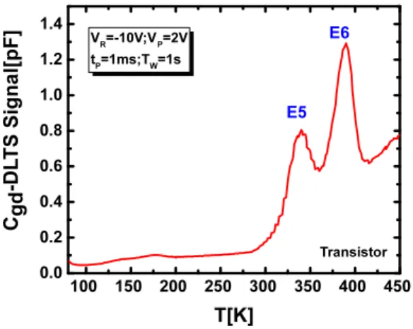
Fig.2: Gate-Drain DLTS measurement of an AlGaN/GaN
MIS-HEMT transistor recorded with VR=0V, VP=2V,
tP=1ms and TW=200ms.
Fig. 3: Gate-Drain DLTS measurement of an AlGaN/GaN
MIS-HEMT transistor recorded with VR=-10V, VP=2V,
tP=1ms and TW=1 s.
The Cgd-DLTS spectrum in Fig. 3 depicts two traps E5(0.64eV) and E6(0.79eV) related to native
defects [6], [8]-[10]. At VR=-10V, the amplitude of E5 is higher than for the case of VR=0V. This could
reveal that the concentration of E5 defect in depth of GaN is higher than the one at the interface. The absence of trap E6 in VR=0V polarization or at least its presence in low density, and contrariwise, its
clear appearance for VR=-10V indicates its deeper position in the GaN buffer layer. This Cgd-DLTS
measurement covers the GaN buffer region between the gate and drain contacts, which can explain the dominance of the defects E5 and E6 related to the native defects in GaN.
2.2.2 Current DLTS
In IDS-DLTS, deep levels are detected by monitoring the drain-current (IDS) changes induced by gate-source-voltage (VGS) pulses. Positive VGS pulses superimposed on negative VGS bias voltage induce electron capture (as VGS=VP is stepped up) and subsequent thermal reemission (after VGS=VR is stepped down to its steady bias value) by deep-level traps located in the 2DEG channel [11].
However, unlike C-DLTS, IDS-DLTS does not provide inherent spatial sensitivity because IDS is
constant throughout the device. Nonetheless, the physical location of defects can be ascertained. By rising VDS voltage, the electrical field lines cover a larger region (Fig. 4b) which causes hot electrons
to scatter out of the channel. These latter hot electrons become trapped in the GaN buffer layers. Fig. 5 shows an IDS-DLTS signal for several drain voltages VDS. Three electron trap signals were
observed, that matches the defect levels E2, E4 and E5 obtained by capacitance DLTS (gate-to-drain configuration) in Fig. 2. This IDS-DLTS measurement covers the channel region in GaN including the zone under the gate, which can explain the dominance of the two defects E2 and E4 related to the gate etching process. In case of VDS=1V, the probed region is too close to the gate and does not cover the
entire region affected by traps E2 and E4 (Fig. 4a). When VDS increases, the probed zone covers the whole region affected by E2 and E4 but also extends into the unintentionally doped GaN (Fig. 4b). That is why the amplitude of the three traps increases but not in the same proportion. By increasing the VDS polarization (up to 5V), the amplitude of E5 defect increases, which confirms that E5 related to gallium vacancy defect is located in the buffer layers.
19th International Conference on Extended Defects in Semiconductors (EDS2018) IOP Conf. Series: Journal of Physics: Conf. Series 1190 (2019) 012013
IOP Publishing doi:10.1088/1742-6596/1190/1/012013
4
Fig.4: The probed region for current DLTS measurements
according to (a) VDS=1V and (b) when VDS increases.
Fig. 5: Current DLTS measurement of an AlGaN/GaN
MIS-HEMT transistor recorded with VR = 0.5V, VP = 3V,
tP = 1ms and TW=1s for several VDS bias.
X
3. Conclusion
Four deep traps were found in multiple-finger normally-off AlGaN/GaN MIS-HEMTs using FT-DLTS. Among these traps, E2 and E4 seems to be formed by the etching process. Traps E5 and E6 are commonly observed in epitaxial GaN and are related to native defects. The localization of these traps has been established by means of capacitance and current deep level transient spectroscopy (DLTS). The Cgd-DLTS measurements show a dominance of E5 and E6 related to native defects in GaN. On the
other hand, the IDS-DLTS measurements reveal a dominance of E2 and E4 related to the gate etching process. Traps E2 and E4 have been localized in the channel close to the gate. E5 and E6 were localized in the GaN buffer layer.
Acknowledgements
This work was done in collaboration with «CEA-LETI» and the funding for this project was provided by a grant from « la Région Rhône-Alpes » via the « ARC4 » (ADR to M. EL KHATIB).
References
[1] G. Meneghesso, M. Meneghini, I. Rossetto, D. Bisi, S. Stoffels, M. Van Hove, S. Decoutere and E. Zanoni, Semicond. Sci. Technol. 2016, 31, 093004.
[2] G. Meneghesso, G. Verzellesi, F. Danesin, F. Rampazzo, F. Zanon, A. Tazzoli, M. Meneghini, E. Zanoni, IEEE Trans. Device Mater. Reliab. 2008, 8, 332.
[3] D. V. Lang, J. Appl. Phys. 1974, 45, 3023. [4] B.W. Wessels, J. Appl. Phys. 1976, 47, 1131.
[5] M. Hrobar, M. Grendel, I. Thurzo, Phys. Status Solidi 1984, 82, 519.
[6] M. El Khatib, P. Ferrandis, E. Morvan, G. Guillot, G. Bremond, Proc. of SPIE 2018, 10532, 1053225.
[7] P. Ferrandis, M. Charles, Y. Baines, J. Buckley, G. Garnier, C. Gillot, G. Reimbold, Jpn. J. Appl.
Phys. 2017, 56, 04CG01.
[8] P. Ferrandis, M. El-Khatib, M.-A. Jaud, E. Morvan, M. Charles, G. Guillot and G. Bremond, J.
Appl. Phys. 2019,125, 035702.
[9] P. Ferrandis, M. Charles, C. Gillot, R. Escoffier, E. Morvan, A. Torres, G. Reimbold,
Microelectron. Eng. 2017, 178, 158.
[10] P. Ferrandis, M. El-Khatib, M.-A. Jaud, E. Morvan, M. Charles, G. Guillot and G. Bremond,
Semicond. Sci. Technol. 2019, 34, 045011.
[11] A. Cavallini, G. Verzellesi, A.F. Basile, C. Canali, A. Castaldini, E. Zanoni, J. Appl. Phys. 2003, 94, 5297.