Publisher’s version / Version de l'éditeur:
Laser & Photonics Review, 4, 2, pp. 283-299, 2010
READ THESE TERMS AND CONDITIONS CAREFULLY BEFORE USING THIS WEBSITE.
https://nrc-publications.canada.ca/eng/copyright
Vous avez des questions? Nous pouvons vous aider. Pour communiquer directement avec un auteur, consultez la première page de la revue dans laquelle son article a été publié afin de trouver ses coordonnées. Si vous n’arrivez pas à les repérer, communiquez avec nous à PublicationsArchive-ArchivesPublications@nrc-cnrc.gc.ca.
Questions? Contact the NRC Publications Archive team at
PublicationsArchive-ArchivesPublications@nrc-cnrc.gc.ca. If you wish to email the authors directly, please see the first page of the publication for their contact information.
This publication could be one of several versions: author’s original, accepted manuscript or the publisher’s version. / La version de cette publication peut être l’une des suivantes : la version prépublication de l’auteur, la version acceptée du manuscrit ou la version de l’éditeur.
For the publisher’s version, please access the DOI link below./ Pour consulter la version de l’éditeur, utilisez le lien DOI ci-dessous.
https://doi.org/10.1002/lpor.200810077
Access and use of this website and the material on it are subject to the Terms and Conditions set forth at
Directed self-assembly of single quantum dots for telecommunication
wavelength optical devices
Dalacu, Dan; Reimer, Michael E.; Frédérick, Simon; Kim, Danny; Lapointe,
Jean; Poole, Philip J.; Aers, Geof C.; Williams, Robin L.; McKinnon, W.
Ross; Korkusinski, Marek; Hawrylak, Pawel
https://publications-cnrc.canada.ca/fra/droits
L’accès à ce site Web et l’utilisation de son contenu sont assujettis aux conditions présentées dans le site LISEZ CES CONDITIONS ATTENTIVEMENT AVANT D’UTILISER CE SITE WEB.
NRC Publications Record / Notice d'Archives des publications de CNRC:
https://nrc-publications.canada.ca/eng/view/object/?id=e0adb9f7-d73d-4e2d-bfcd-ffe86e01330a https://publications-cnrc.canada.ca/fra/voir/objet/?id=e0adb9f7-d73d-4e2d-bfcd-ffe86e01330aLASER &
PHOTONICS
REVIEWS
Abstract The ability to control the nucleation site of a single quantum dot will have a profound effect on the development of quantum dot-based photonic devices. The deterministic ap-proach will provide a truly scalable technology that can take full advantage of conventional semiconductor processing for device fabrication. In this review, we discuss the progress towards the integration of deterministically nucleated single quantum dots with top-down quantum optical devices targeting telecommuni-cation wavelengths. Advances in site-controlled quantum dot nucleation using selective-area epitaxy now makes it possible to position quantum dots at predetermined positions on a substrate in registry with alignment markers. This, in turn, has allowed for devices fabricated in subsequent processing steps to be aligned to individual quantum dots. The specific devices being targeted are gated-single dots and coupled dot-cavity systems which are key components of efficient sources of single photons and
entangled photon pairs. A gated InP pyramid containing a single InAs quantum dot.
© 2010 by WILEY-VCH Verlag GmbH & Co. KGaA, Weinheim
Directed self-assembly of single quantum dots for
telecommunication wavelength optical devices
Dan Dalacu1,*, Michael E. Reimer1,2, Simon Fr´ed´erick1,3, Danny Kim1,4, Jean Lapointe1, Philip J. Poole1, Geof C. Aers1,
Robin L. Williams1,2, W. Ross McKinnon1, Marek Korkusi´nski1, and Pawel Hawrylak1,2
1
Institute for Microstructural Sciences, National Research Council, Ottawa, Canada, K1A 0R6
2
Department of Physics, University of Ottawa, Ottawa, Canada, K1N 6N5
3
Walter Schottky Institut and Physik Department, Technische Universit¨at M¨unchen, 85748 Garching, Germany
4
Naval Research Laboratory, Washington, DC 20375, USA
Received: 5 December 2008, Revised: 24 March 2009, Accepted: 25 March 2009 Published online: 23 April 2009
Key words: Site-selective epitaxy, quantum dots, single photon sources. PACS: 73.21.La, 71.35.-y, 78.67.Hc, 78.55.Cr
1. Introduction
Quantum dots, known as artificial atoms, are 3D islands of lower bandgap semiconductor embedded within a higher bandgap semiconductor matrix. The 3D confinement of electrons and holes results in a discrete energy-level spec-trum reminiscent of atomic systems [1]. Self-assembled quantum dots are grown through the Stranski-Krastanow growth mode [2] in which 3D islands nucleate sponta-neously after a few monolayers of normal 2D growth of compressively strained layers. To date, the most widely
studied quantum dots are based on the InAs/GaAs material system [3]. These dots typically emit around 1 µm, although pseudomorhpic InGaAs/GaAs dots emitting at 1.3 µm have been demonstrated [4]. Less studied but more relevant to fibre-based applications targeting telecommunication wave-lengths is the InAs/InP quantum dot system [5–7] which can emit at 1.3 µm and 1.55 µm.
One particular application of quantum dots relates to nonclassical light generation. Sources that can generate pure single-photon states on demand [8,9] form the basis of future technologies in the field of quantum information
cessing. Owing to their atomic-like energy spectrum, quan-tum dots can be regarded as a two-level quanquan-tum system [1] that can generate exactly one single photon, or entangled photon pair, per excitation trigger pulse. After relaxation, the quantum system is necessarily in its ground state, and can not emit until the next excitation pulse. Antibunched emission, a signature of single photon emission, has been observed in both the InAs/GaAs [10–14] and InAs/InP [15] material systems.
The atomic-like properties alone do not secure quan-tum dots as a viable approach to nonclassical light genera-tion. Efficient devices require the quantum dot to be placed in a single mode, high finesse, small volume microcav-ity [16, 17]. The cavmicrocav-ity serves to modify the photon emis-sion dynamics [18] enhancing device efficiency [17, 19, 20], as well as directing the emission from the dot for efficient coupling to an external optical system. It is the ease with which quantum dots can be integrated with monolithic semi-conductor devices that makes them promising as a scalable technology for single and entangled photon pair generators.
However, the self-assembly of quantum dots is, by na-ture, a random process and the lack of spatial control of dot nucleation severely hinders the deterministic integration of quantum dots and top-down devices such as cavities. Initial studies on dot-cavity systems [11, 12, 14] used low dot density samples, and large arrays of cavities, relying on statistics in order to find a resonant single dot - cavity sys-tem. More recently, deterministic dot-cavity coupling [21] has been achieved by registering the position of pre-selected quantum dots from a randomly nucleated ensemble using various methods [21–23] and fabricating tailored microcav-ities at the dot site.
Ideally, one would like to nucleate the quantum dots at predetermined positions on the substrate to facilitate subse-quent device fabrication. Early attempts at site-controlled nucleation based on selective-area epitaxy were done in the nineties [24–26] and have since been refined [27–31] and expanded to include other surface modification tech-niques [32–34] (for a recent review, see [35]. These efforts have led to the deterministic nucleation of high optical quality single dots [31–33, 36] capable of single photon emission [31, 32].
The maturing site-control technology has naturally led to quantum dot nucleation in registry with marker structures that permit alignment of devices fabricated in subsequent processing steps [37]. This approach has been used for the deterministic integration of quantum dots with top-down devices such as cavities [38–40] and gated structures [41], the latter used for electric field tuning of the dot charge state [42] or manipulation of the electron and hole wave-functions [43, 44].
In this article, we review the directed self-assembly of InAs quantum dots using InP nanotemplates [27, 45, 46] as a route to deterministic quantum dot devices targeting telecommunication wavelengths. The nanotemplating pro-cess, based on selective-area epitaxy, is described and site-controlled nucleation is demonstrated. Progress on quantum
dot size and shape control through nanotemplate geometry is reported.
The directed self-assembly process is used to demon-strate deterministic integration of site-controlled quantum dots with top-down devices relevant to nonclassical light generation. Site-controlled quantum dots are incorporated into field effect devices [41] and high finesse, small volume microcavities. In the first example, deterministically posi-tioned quantum dots are placed between Schottky gates for the application of vertical and lateral electric fields. Ver-tical fields permit the control of the exciton charge state whilst lateral fields can be used to overcome the limitation on polarization entangled photon pair generation [47] due to the natural asymmetry of the quantum dot [48]. In the second example, a process is described that would allow for the deterministic integration of a 2D photonic bandgap cavity with a single quantum dot. The process is applica-ble not only to dot-cavity systems, essential in regard to device efficiency [16, 17], but also to cavity-waveguide con-figurations, relevant to input-output coupling with external optical systems.
2. Directed self-assembly
The directed self-assembly of quantum dots can be viewed as the control of the nucleation process by virtue of the facet-dependant adatom surface migration using a nanotem-plate [27, 45, 46]. The nanotemnanotem-plate allows one to attain dimensions necessary to restrict nucleation down to a sin-gle dot starting from dimensions readily obtained using electron beam (ebeam) lithography. Fabrication of the nan-otemplate is based on patterned-substrate growth, and is thus an✐♥s✐t✉ process providing a clean, defect-free sur-face for dot nucleation. The process relies on several factors related to the particulars of growth on a patterned substrate, including selectivity and relative incorporation rates.
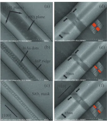
The starting point for the directed self-assembly pro-cess for InAs dots on InP is a SiO✷coated (001) InP wafer which has been ebeam patterned and wet etched to produce openings of width✇♦in the oxide, shown schematically in Fig. 1a. The oxide is only 20 nm thick to limit shadow-ing of the source material durshadow-ing growth and to preserve the ebeam pattern after the isotropic wet etch. The first of several aspects of patterned-substrate epitaxy critical to nan-otemplate fabrication is the selective nature of the growth. Using chemical beam epitaxy [5] with trimethyl-indium and cracked PH✸sources, conditions can be found that re-sult in growth exclusively on the exposed InP and not on the SiO✷mask. Second, if the openings in the oxide are aligned to specific crystallographic directions, the sidewall facets that develop during growth are crystallographic planes, and as such, are smooth, defect-free, and reproducible. Fig. 1b shows schematically the patterned-substrate growth in a [100] oriented stripe where the sidewalls are❢✶✶✵❣ planes.
The final aspect in the nanotemplate growth is the pref-erential migration of the group III species. The migration length of In adatoms is longer on the higher index facets
SiO2 InP InAs (a) (c) (d) [001] [010] [100] w o w (001) {110} (b)
Figure 1 (online color at: www.lpr-journal.org) Schematic of the directed self-assembly pro-cess: (a) patterned-substrate used for the nanotemplate growth, (b) nanotemplate obtained from InP growth on the patterned-substrate, (c) self-assembled dots grown on the nanotemplate, and (d) capped sample.
and, as such, they migrate off the❢✶✶✵❣ sidewalls and incor-porate on the top (001) plane. The result is the ridge shown in Fig. 1b, which is confined to the oxide opening, with no lateral growth on the❢✶✶✵❣ planes, and a top (001) facet re-duced to a width of✇.. Continued growth would complete the ridge with the elimination of the (001) plane, and lateral growth would commence, with the ridge overgrowing the oxide. For the nanotemplate, however, the ridge growth is stopped when the (001) plane is reduced sufficiently to di-rect the assembly of the quantum dots to the desired extent, as in Fig. 1b.
Since it is the group III species that dictates the incorpo-ration in III-V epitaxy, the deposition of InAs proceeds as does the InP, with the In adatoms migrating to the top (001) facet. Dot formation via the Stranski-Krastanow growth mode [2] occurs for InAs deposited in amounts exceeding the critical thickness, as shown schematically in Fig. 1c. Since growth proceeds by material deposition on the (001) surface and collection from the sidewalls, simple geomet-ric considerations [45] give a growth rate that exceeds the planar growth rate by up to a factor of✇♦❂✇; the ratio of the ridge base to ridge top. As such, the amount of InAs required for dot formation on the nanotemplate will de-pend on the geometry of the ridge which is dictated by the amount of InP deposited and the width of the stripe.
For optical characterization, the dots are capped with InP as shown in Fig. 1d. For structural characterization the quantum dots are left uncapped, keeping in mind that the capping process will modify the dots [45]. Plan view scanning electron microscopy (SEM) images of uncapped [100] oriented ridges of different base widths are shown
Figure 2 (online color at: www.lpr-journal.org) Left panel: (a– c) plane view SEM images of uncapped nanotemplate ridges aligned along the [100] direction. Right panel: (d–f) ridges aligned along the [0✖✶0] direction that have been repatterned to limit the nucleation of only one or two dots. The insets are schematics of the one and two dot configurations.
in the left panel of Fig. 2. Smooth, defect-free (001) and ❢✶✶✵❣ facets are evident. The three ridges were deposited in the same growth so that smaller openings result in smaller (001) top widths. Narrowing of the top width affects the dot formation in two ways. First, the amount of deposited material on the (001) top plane increases as✇♦❂✇ increases, and, as such, the dot height increases, as can be inferred from the contrast in the SEM images. Second, the decreased top width increases the spatial confinement and gives rise to dot ordering to the point where only a single row of dots will fit on the top (001) facet.
Although instructive for understanding the nanotem-plate growth process, ridges are not useful for the produc-tion of single dot devices. To obtain single dots from ridge structures, an additional patterned-substrate growth is re-quired. InP ridges are grown as before, but no dots are deposited. The nanotemplate is re-patterned with stripes perpendicular to the ridges, leaving the original oxide mask on. This leaves only a segment of the ridge exposed, the width of which can be reduced to the limits of the lithog-raphy. The InAs deposition is carried out as before, with the addition of an initial thin buffer layer of InP. SEM im-ages of three double-patterned ridges are shown in the right panel of Fig 2. In Fig. 2d, the second strip width is 120 nm, which is sufficient to allow the nucleation of only two dots along the ridge for✇ ❂ ✼✵ nm. Reduction of the second stripe width to 80 nm, as in Fig. 2e, limits the growth to
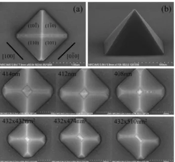
Figure 3 Upper panel: (a) top and (b) side views SEM images of a completed nanotemplate pyramid orient along the ❤✶✵✵✐ directions. Uncapped pyramidal nanotemplates in square (middle panel) and rectangular openings (lower panel), each supporting a single quantum dot.
a single dot. For a slighter wider ridge,✇ ❂ ✽✺ nm, as in Fig. 2f, two dots can again be supported, in this case, the dot molecule is aligned perpendicular to the ridge.
Ideally, one would like to spatially isolate a single dot using a single patterned-substrate growth. This can be achieved by replacing the stripe geometry with squares. Instead of ridges, growth in square openings results in pyramid structures with four crystallographic planes as sidewalls. For an opening with sides aligned along❤✶✵✵✐ directions, the four sidewalls are❢✶✶✵❣ planes. Growth of a completed pyramid in a❤✶✵✵✐ oriented square is shown in the top panel of Fig. 3, showing, again, smooth defect-free sidewalls inherent to crystallographically determined side-walls.
As with ridges, directed self-assembly using square openings entails dot deposition prior to pyramid completion. Using small incremental steps in the patterning, not only can the nucleation site of a single dot be spatially controlled, but also the lateral dimensions of the dot. This is shown in the middle panel of Fig. 3 where the base width of the pyramid is reduced from 414 nm to 408 nm. In each case, the top (001) apex of each pyramid only supports a single dot. Reducing the size of the top apex increases the spatial confinement of the dot, thus reducing its size. Again, the dot height increases for reduced lateral dimensions as✇♦❂✇ increases. One can go further and control the shape of the dot simply by using a rectangular geometry. This is shown in the lower panel of Fig. 3 where the aspect ratio of the rectangular opening is increased from 1 to 1.18. In each case, the pyramid apex contains only a single dot, the shape of which follows the geometry of the opening.
Fig. 3 highlights the versatility of the nanotemplate pro-cess. Not only can the spatial location of a single dot be controlled, but also, by virtue of the nanotemplate geometry, the dot size and shape as well. Control of the dot dimen-sions allows tuning of the electronic structure of the dot, and thus the emission energies and level spacings [49]. This is of particular relevance to entangled photon pair genera-tion [50–53], where the dot size and shape will determine whether the photon polarizations are entangled, or simply correlated [47].
3. Optical spectroscopy
Since the growth is completely selective, with the position of features controlled by the lithography, the nanotemplate structures can be separated by distances large enough to allow optical measurements to be readily performed on individual structures. The optical spectroscopy of the nan-otemplate structures is further simplified due to their high visibility in an optical microscope. Pyramidal nanotem-plates need no further processing, however, ridge structures of the type in Fig. 2a–c require deposition of a metal mask consisting of two metal gates separated by a small gap. The mask is necessary to isolate emission from only a short length of the ridge. Optical measurements are done at 4.2 K in a continuous flow helium cryostat using non-resonant, above bandgap excitation through a microscope objective. The luminescence is collected through the same microscope objective, dispersed using a single grating spectrometer and detected using a liquid-nitrogen cooled InGaAs diode array.
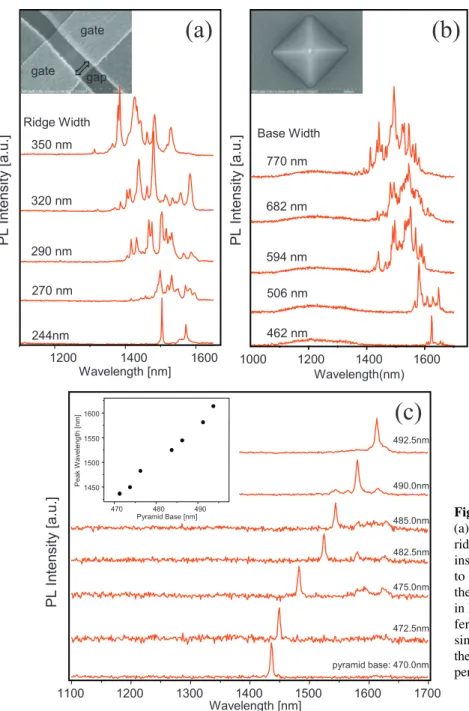
The photoluminescence (PL) from gated ridges of dif-ferent base widths grown in the same run is shown in Fig. 4a. Ridges with large base widths, expected to contain many dots, show a broad distribution of peaks centered around 1500 nm, typical of InAs/InP quantum dots [5]. As the ridge width is decreased, one expects a reduction in the number of dots and an increase in dot height. In the PL spectra, the latter corresponds to a progressing redshift of the emission spectrum, and the former to a progressive simplification of the spectrum. For sufficiently narrow gate gaps the re-duction of the top width leads to isolation of a single dot, the signature of which is a single dominant peak in the emission as observed in the bottom spectrum of Fig. 4a.
The luminescence spectra from pyramid structures as a function of base width is shown in Fig. 4b. Similar to the ridges, the PL shows a progressive redshift and a reduc-tion in the number of emission peaks with decreasing base width. For the smallest base width, the spectrum simplifies to a single peak associated with the emission from a sin-gle dot. The broad emission around 1.25 µm originates for impurity-related defects in the semi-insulating Fe-doped InP substrate. It is not evident in the ridge samples as a significant proportion of the substrate is covered by the Au gates.
From the middle panel in Fig. 3, there is a small range of pyramid sizes where one can expect control of the lateral dimensions of individual dots. The emission from single
gate gate gap 1000 1200 1400 1600 Wavelength(nm) 594 nm 506 nm 682 nm 462 nm 770 nm Base Width PL I n te ns it y [a.u.] 1200 1400 1600 PL I n te ns it y [a.u.] Wavelength [nm] 290 nm 270 nm 320 nm 244nm 350 nm Ridge Width
(a)
(b)
PL I n te ns it y [a.u.] 1100 1200 1300 1400 1500 1600 1700 Wavelength [nm] 492.5nm 490.0nm 485.0nm 482.5nm 475.0nm 472.5nm pyramid base: 470.0nm 470 480 490 1450 1500 1550 1600 P eak W a vel ength [nm ] Pyramid Base [nm](c)
Figure 4 (online color at: www.lpr-journal.org) (a) Photoluminescence from InAs dots in InP ridge nanotemplates of different base width. The inset shows an SEM image of a gated ridge used to isolate the emission from only those dots in the gap. (b) Photoluminescence from InAs dots in InP pryamidal nanotemplates (see inset) of dif-ferent base width. (c) Photoluminescence in the single dot regime for small incremental steps in the pyramid base width. The peak wavelength de-pendence on the base width is shown in the inset.
dot pyramids as the base dimension is reduced in small steps is shown in Fig. 4c for a sample grown on a S-doped substrate. The inset shows the peak wavelength blue-shift from 1614 nm to 1436 nm as the pyramid base is reduced from 492.5 nm to 470 nm. The blue-shift is consistent with increased lateral confinement as the dot’s lateral dimensions are reduced. These early studies are promising in regard to controlling the emission energy of individual quantum dots through nanotemplate geometry.
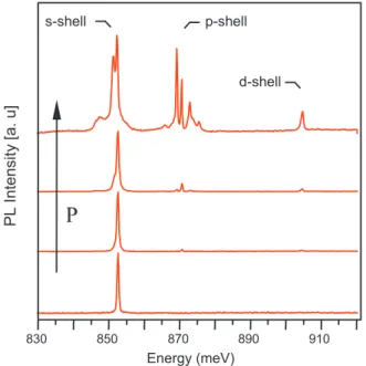
The electronic structure of single quantum dots is eluci-dated from the power dependent emission [54]. Fig. 5 shows the photoluminescence data collected as a function of exci-tation power from a single dot on a pyramidal nanotemplate. The spectra have been offset along the② axis for clarity of
presentation. At the lowest pump powers, a single peak at 852 meV is observed and identified as the recombination from a single exciton occupying the doubly spin degenerate s shell for which the orbital angular momentum, ▲ ❂ ✵. The linewidth of the exciton peak is resolution-limited to 60 µeV, similar to measurements on randomly nucleated InAs/InP dots [55], indicating that the optical quality of the dots is not affected by the nanotemplate process. At higher excitation intensity, a second emission line appears ✘ ✶ meV below X which is identified as the biexciton (XX), or single exciton annihilation in the presence of a second exciton of opposite spin. The 1 meV splitting is a result of Coulomb-induced renormalization, and can be viewed as the biexciton binding energy.
830 850 870 890 910 PL Intens it y [a. u] Energy (meV) s-shell p-shell d-shell
P
Figure 5 (online color at: www.lpr-journal.org) Photolumines-cence from a single InAs quantum dot as a function of excitation power for a dot in a pyramidal nanotemplate with bounds, ♣ and ❞ orbitals.
Concomitant with the appearance of the biexciton is the first excited state, the♣ shell, at 871 meV. For group ❉✷❞
symmetry, the♣ shell is characterized by doubly degener-ate,▲ ❂ ✝✶, single particle levels for both electrons and holes that can accommodate a maximum of four optically active excitons. The♣ shell in Fig. 5 reflects transitions associated with this 3X-6X occupation, at energies renor-malized by Coulomb interactions. The complexity of the ♣-shell emission is associated with a reduced symmetry of the dot [49] and concomitant mixing of the▲ ❂ ✝✶ states which removes the level degeneracy. A final additional peak at 905 meV appears at higher pumping powers and is associated with a transition from the❞-shell of the dot.
The▲ ❂ ✵ single particle levels for both electrons and holes can accommodate two optically active excitons. The two excitonic levels contributing to this peak are degenerate for complete rotational symmetry in the plane, group❉✷❞. The reduced symmetry lifts the degeneracy due to electron-hole exchange interaction [48] and leads to polarization dependent exchange splitting for the exciton. The fine struc-ture, or anisotropic exchange splitting (AES), is shown in the exciton and biexciton emission spectrum in Fig. 6. The two orthogonally polarized peaks contributing to the exci-ton emission at 843.7 meV are resolved by measuring the polarized PL from dot. The peaks contributing to the biexci-ton emission at 840.5 meV are similarly resolved, with the sign of the AES opposite that of the exciton. This behavior is expected from the biexciton cascade (see energy level diagram in Fig. 11) and will be discussed in more detail in Section IV. The inset in Fig. 6 shows the emission energy of the exciton, determined by fitting a single lorenzian to the
0 90 180 270 360 843.7 843.8 843.9 E n ergy (m e V )
Polarization angle [deg]
835 840 845 850 Horizontal polarization Vertical polarization Ph ot ol umi n esc enc e In tens it y [a.u.] Energy (meV) XX X X PLB1 PLA1 PLA2 PLB2
Figure 6 (online color at: www.lpr-journal.org) Emission from exciton complexes (X, XX, and X ) from a single InAs quan-tum dot showing polarized anisotropic exchange splitting of the exciton and biexciton lines. The inset shows the polariza-tion dependent emission of the exciton from which a value of ✁❆❊❙❂ 200 µeV is obtained. PL❆✶, PL❇✶, PL❆✷, and PL❇✷ cor-respond to transitions A1, B1, A2, and B2 in Fig. 10, respectively.
PL peak, as a function of polarization angle of a half-wave plate at the input of the monchromater. Using this method, splittings below the resolution of the spectrometer can be determined, and a value of✁❆❊❙ ❂ 200 µeV is obtained for this particular dot.
PL from single dots typically contain multiple emission lines corresponding to recombination of excitons with more than one charge state [56]. This is highlighted in Fig. 6 in which emission from a third peak is visible at 839.5 meV and identified as a negatively charged exciton, X , corre-sponding to electron-hole recombination in the presence of an additional electron. The Coulomb-induced renormal-ization results in an emission energy 4.2 meV below that of the exciton and, contrary to emission from the neutral exciton complexes, X does not possess any fine structure splitting [48].
Emission from exciton complexes of varying charge can arise from fluctuations in the local electronic environ-ment of the dot which effect the position of the Fermi level with respect to the quantum dot energy levels. Ideally, one would like to control the exciton charge state on an indi-vidual quantum dot. This can be accomplished utilizing metal-oxide-semiconductor or metal-semiconductor struc-tures whereby tunneling of the electrons in and out of the quantum dot is achieved via electric fields [42, 57–62]. A single quantum dot in a pyramidal nanotemplate forms an ideal geometry for devices requiring metal gates for applica-tion of electric fields and optical access for PL spectroscopy. Vertical fields can be applied across the intrinsic region of the pyramid using Au/Ti Schottky gates on the sidewalls of the pyramid and an n-doped substrate serving as a back
con-tact [41, 63]. An SEM image of a typical device is shown in the title figure where gates have been deposited on each of the four❢✶✶✵❣ sidewalls of the pyramid.
The Schottky gates are fabricated using an e-beam de-fined poly(methyl methacrylate) (PMMA) lift-off process, with alignment provided by trenches dry-etched into the substrate 50 µm from the pyramid. There is one pyramid per ebeam write field and each field contains a set of align-ment trenches providing independent alignalign-ment and true scalability. The gates are typically aligned with an accuracy of better than 50 nm to the apex of the pyramid as shown in plan view SEM images in Fig. 7a.
812 814 816 818 820 822 824 826 -2.5 -2.0 -1.5 -1.0 -0.5 0.0 Energy [meV] Gate Vol tage [ V ]
X
X
X
2 Vg SiO2 Ti/Au n-InP(a)
(b)
Figure 7 (online color at: www.lpr-journal.org) (a) SEM plan view image of a gated pyramid. (b) Contour plot of PL spectra as a function of bias applied to the top four gates. Single electron charging is evident from the discrete jumps in the emission energy at✘ 0.5 V and ✘ 1.5 V. The inset is a schematic of the cross-section of the device.
Vertical electric fields for single electron charging are obtained by biasing all four top gates relative to the back ohmic contact. A schematic of the cross-section of the n-i-Schottky diode configured for vertical fields is shown in the inset of Fig. 7b. Fig. 7b shows a contour plot of the PL spectra as function of bias applied to the top gates for a single dot in a pyramidal nanotemplate. At zero bias a dominant peak at 819.2 meV and a weaker satellite at 813.4 meV are observed. With increasing reverse bias there are discrete jumps in emission energy at particular voltages signifying single electron charging events. At high bias the emission from the dot quenches as the tunneling rate of photoexcited carriers out of the dot exceeds their radiative lifetime and carriers contribute to photocurrent.
The statistical nature of carrier capture processes for nonresonant excitation results in the coexistence of differ-ent charge states. One can iddiffer-entify, however, bias plateaus for which there is emission from only one charge state. Spectra from three such biases are shown in Fig. 8. The bottom spectrum is taken under high reverse bias condi-tions (❱● ❂ ✶✿✽❱ ) such that the Fermi level, ❊❋, in
the n-InP back contact lies below the energy levels of the dot. The dot, therefore, is empty of carriers, and the ob-served peak corresponds to the neutral exciton emission. With decreasing reverse bias, the bands flatten and the en-ergy levels in the dot are shifted below❊❋ resulting in
Energy [meV] PL In te n s ity [a .u .] VG=0V
X
2-n-sc EFX
VG=-1.8V VG=-1.1VX
-820 830 810 815 825Figure 8 (online color at: www.lpr-journal.org) PL spectra at biases corresponding to different charge states. Lefthand insets: band profiles under negative bias conditions. Righthand insets: configuration of the initial states involved in the transitions.
15 20 25 30 35 40 45 50 823.3 823.5 823.7 823.9 824.1 824.3 -0.5 -1.0 -1.5 -2.0 -2.5
X
X
-Ener gy (meV) Electric field (kV/cm) Gate Voltage [V]Figure 9 (online color at: www.lpr-journal.org) Emission en-ergies of X (black squares) and X (blue circles) as a function of vertical electric field. X has been offset by a constant energy to obtain a quadratic fit for both complexes simultaneously. The solid curve is a fit to❊ ❂ ❊✵✰ ♣❋ ✰ ☞❋✷
successive single electron charging. The second spectrum at❱● ❂ ✶✿✶❱ corresponds to the X emission whilst the third at❱●❂ ✵❱ is the doubly charged exciton, X✷ , corresponding to electron-hole recombination in the pres-ence of two additional electrons. The two emission lines from the X✷ relaxation is a consequence of two possible final states with parallel or anti-parallel spin orientations of the two remaining electrons and the concomitant dif-ference in s-p exchange energies [54, 61, 64]. The specific carrier occupation of the dot at each bias is a consequence of the particular geometry of the device together with the substrate doping and background carrier concentration in the pyramid [63].
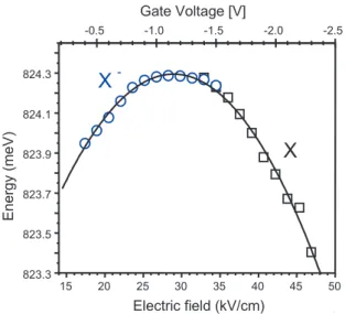
As well as single electron charging, an applied bias redshifts the energies of the exciton complexes due to the quantum confined Stark effect [65]. Fig. 9 shows the emis-sion energies of X and X as a function of applied field, with an offset added to X assuming a negligible reduction in dipole due to the additional electron [60]. The field is calculated by simultaneously solving Poisson’s equation and the continuity equations for electrons and holes, whilst utilizing the drift diffusion model for charge transport [63].
The Stark shift of the exciton complexes provide in-formation on the nature of carrier wavefunctions and, by comparison with theory, on the composition and geome-try of the dots [66]. The emission energy dependence on vertical field is well described by
❊ ❂ ❊✵✰ ♣❋ ✰ ☞❋✷✿ (1) where ❊✵ is the emission energy at zero field, ☞ is the polarizability of the electron and hole states responsible for the Stark shift, and♣ ❂ ❡r is the permanent excitonic dipole moment where ❡ is the electron charge and r is
the electron-hole separation. Fitting Eq. (1) to the data in Fig. 9 gives a built-in dipole♣❂❡ ❂ ✶✿✺✽ nm and a Stark shift☞ ❂ 2.7 µeV cm2/kV2. The built-in dipole results in an asymmetric Stark shift, peaking not at zero field, but rather at❋ ❂ ✸✵ kV/cm. The direction of the dipole is from dot apex to base and implies an electron charge density distribution that is above that of the hole at zero field [67]. This vertical electron-hole separation is consistent with a uniform In composition in the dot, contrary to InAs dots on GaAs where Ga diffusion must be assumed to account for a dipole directed from dot base to apex [66, 68].
4. Optical devices
4.1. Non-classical light sources
The ideal source of single photons should generate single photons on demand with a short dwell time between suc-cessive photon generation events and with✶✵✵✪ efficiency; every generated photon being collected by an optical sys-tem. The atomic-like density of states of quantum dots is a prerequisite for nonclassical light emission. If a photon is emitted from recombination of an excited state of the dot at✜ ❂ ✵, it is impossible for the dot to emit another photon immediately after, since it is necessarily in the ground state. On demand emission is provided by pulsed excitation, the dwell time determined by the excitation used and the excita-tion recombinaexcita-tion rate. It is the exciton recombinaexcita-tion that has been used to demonstrate single photon emission in the InAs/GaAs material system using second-order correlation spectroscopy for both randomly nucleated [10, 11, 13, 14] and site-controlled quantum dots [31, 32]. Demonstration of single photon emission from InAs/InP quantum dots [15] has proved more difficult due to the inferior performance with respect to dark counts of single photon InGaAs detec-tors compared to Si CCD devices.
For entangled photon pair generation, the sequential emission of photons from the biexciton and exciton decay has been proposed [69]. The process is shown schematically in Fig. 10a for a symmetric dot (❉✷❞symmetry group) for
which✁❆❊❙ ❂ ✵. The biexciton-exciton cascade emits
two contra-circularly polarized photons, either✛✰✛ or ✛ ✛✰, depending on which decay path (A or B) via the
intermediate two-fold degenerate exciton states (❥❳✶✐ or
❥❳✷✐) is taken. Since the path, and hence the polarization,
of the first and second photon, is unknown, the appropriate quantum mechanical description is the superposition of both probabilities, namely a polarization entangled photon pair✠ ❂ ♣✶
✷✭✛✰✛ ✰ ✛ ✛✰✮.
Entanglement in these schemes is destroyed, however, if the degeneracy of the two possible spin configurations of the intermediate neutral exciton ground state is lifted [47]. In anisotropic quantum dots the electron-hole exchange interaction splits the two excitonic states by✁❆❊❙(see in Fig. 10b) giving which-path information in the energy of the emission. There have been extensive efforts to remove
XX X1 vacuum 0 σ+ σ -σ -σ+ ∆AES
A
1B
1A
2B
2A
1B
1A
2B
2 HXX HX VXX VX X2 XX X1 vacuum 0 X2(a)
(b)
Figure 10 (online color at: www.lpr-journal.org) Schematic diagram of the biexciton-radiative cas-cade (a) a symmetric dot with✁❆❊❙❂ ✵ and (b) an asymmetric dot with zero biexciton binding energy such that PL❆✶❂ PL❇✷and PL❇✶❂ PL❆✷.
the✁❆❊❙through the application of external magnetic [70] and electric [43, 44] fields, or through spectral filtering [71], applied uniaxial stress [72], and quantum size and compo-sition engineering [50–53].
An alternative scheme [73,74] involves manipulation of the biexciton binding energy. Consider a quantum dot for which the biexciton binding energy is zero. In this case, the peak energies PL❆✶and PL❇✷in Fig. 6 are degenerate, as are PL❇✶and PL❆✷. In the energy level diagram of Fig. 10b this corresponds to two pairs of degenerate transitions, the ❆✶ ❇✷pair and the❇✶ ❆✷pair. These two pairs, being degenerate, provide two indistinguishable recombination pathways for the biexciton even in the presence of non-degenerate intermediate exciton states. In the presence of a non-zero✁❆❊❙, the two-photon wave function is entangled in the horizontal (H) and vertical (V) polarization degrees of freedom✠ ❂ ♣✶
✷✭❱❳❳❱❳✰ ❍❳❳❍❳✮.
The biexciton binding energy can be removed by pre-cisely balancing the competing Coulomb attractions and repulsion for excitons and biexcitons using an applied lat-eral electric field. The two optically active exciton states have energies
❊❳✶❀❳✷❂ ✎❡✵✵✰ ✎❤✵✵ ❱❡❤✵ ✁❊❳❝♦rr✞✁❆❊❙✷ (2)
where ✎❡✵✵ ✰ ✎❤✵✵ are the single particle energies, ❱❡❤✵ is the electron-hole attraction, and✁❊❳❝♦rr the correlation energy. Since the final state in the excitonic recombination is the vacuum, the above energies also define the PL peak positionsP ▲❆✷andP ▲❇✷. With an applied lateral field, P ▲❆✷andP ▲❇✷decrease due to a reduction in the single
particle energies (Stark shift). The redshift is small since it is compensated by a decrease with applied field of the electron-hole attraction and the correlation energy terms.
Similarly, the biexciton energy can be approximated by
❊❳❳ ❂ ✷✎❡✵✵✰✷✎❤✵✵✰❱❡❡✵✰❱❤❤✵ ✹❱❡❤✵ ✁❊❳❝♦rr✝✁❆❊❙✷ ✿
(3)
The energies of the photons emitted in transitions❆✶and ❇✶are given byP ▲❆✶❀❇✶❂ ❊❳❳ ❊❳✶❀❳✷: P ▲❆✶❀❇✶❂ ✔ ✎❡ ✵✵✰ ✎❤✵✵ ❱❡❤✵ ✁❊❳❝♦rr✝✁❆❊❙✷ ✕ ✰✂❱✵ ❡❡✰ ❱❤❤ ✷❱❡❤✵ ✄ ❬✁❊❝♦rr ❳ ✷✁❊❳❳❝♦rr❪ ✿ (4)
The first term in Eq. (4) is identical to Eq. (2) but with oppo-site contribution from the❆❊❙. The second term accounts for Coulomb interactions between the two electron-hole pairs building the biexciton and is approximately zero at zero field, since repulsion between like carriers is balanced by electron-hole attraction. The third term, comparing the correlation corrections of the biexciton to those of the ex-citon, defines the splitting between the PL lines of the two complexes. The field-driven separation of the electrons and holes decreases the electron-hole attraction driving the biexciton PL peak positions towards higher energies. For a sufficiently large electric field the interaction terms exactly cancel the correlation corrections, resulting in a degeneracy of the biexciton and exciton emission. Results from Full Configuration Interaction calculations [73, 74] are shown in Fig. 11a where the redshifting exciton and blueshifting biexciton result in removal of the biexciton binding energy at a field of 6.5 kV/cm.
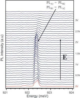
Photoluminescence experiments under applied electric field were performed on a gated ridge sample, the gates serving the dual purpose of isolating emission from a single dot and as Schottky gates for applying a lateral field. The spectra as a function of applied field are shown in Fig. 12 for an excitation intensity chosen to excite only the two neutral exciton ground states split by the electron-hole ex-change. From 0 V to 1.9 V, a small Stark shift is observed, with✁❆❊❙decreasing from 108 µeV to 56 µeV. At approx-imately 1.9 V, the X transition is crossed by the XX peak and corresponds to zero biexciton binding energy. The biex-citon continues to blueshift with further increases in bias,
0 1 2 3 4 5 6 7 8 9 0 1 2 3 En er g y ( m eV) Electric field (kV/cm) PLA1 = PLB2
X
XX
0.0 0.5 1.0 1.5 2.0 2.5 3.0 3.5 4.0 921.6 922.0 922.4 922.8 En er g y ( m eV)Bias voltage (Volts)
X
XX
PLB1 = PLA2
PLA1 = PLB2
PLB1 = PLA2
Figure 11 (online color at: www.lpr-journal.org) (a) Calculated PL transitions for the exciton and biexciton as a function of lateral electric field obtained from Fermi’s golden rule. (b) Peak energies extracted from Fig. 12 as a function bias voltage. X and XX are colour coded in the same manner used in (a).
921 922 923 924 PL i nt ens it y ( a.u) Energy (meV) 2V 1V 1.5V 0V 0.5V 3V 2.5V
E
PLA1 = PLB2 PLB1 = PLA2Figure 12 (online color at: www.lpr-journal.org) Electric field dependent PL spectra from a single quantum dot in a ridge nan-otemplate. For biases less than 1.9 V, the doublet corresponds to the two exciton transitions, whilst for biases greater than 1.9 V, the observed peak corresponds to the biexciton transition.
eventually disappearing due to the decreasing overlap be-tween the electron and hole wavefunctions and concomitant reduction of the oscillator strength of the transition. The field dependence of the exciton and biexciton energies is shown more clearly in Fig. 11b where the peak positions have been extracted from the PL spectra in Fig. 12. The field-induced shifts of the exciton and biexciton transitions have been colour-coded in the same manner as in Fig. 11a to facilitate comparison between the theory and experiment which are in qualitative agreement.
4.2. Microcavities
Quantum dots may generate non-classical light, but, by themselves, would make for very inefficient sources con-sidering the difficulties in extracting light from high index materials [75]. Efficient devices necessitate the coupling of a transition dipole of the dot to a single mode of a 3D microcavity [19,20]. The efficiency of collection is dictated by the ability to couple, both spectrally and spatially, the quantum dot and the cavity mode, as well as properties re-lated to the cavity mode itself. The collection efficiency can be quantified by calculating the spontaneous emission rate of a transition dipole of the dot into the cavity mode,✶❂✜❝, referenced to the total spontaneous emission rate in a homo-geneous medium,✶❂✜. The spontaneous emission rate of a transition dipole at positionr❡calculated in perturbation theory is given by [76] ✜ ✜❝ ❂ ✸◗✭✕❝❂♥✮✸ ✹✙✷❱ ✍✦✷ ❝ ✹✭✦❡ ✦❝✮✷✰ ✍✦❝✷ ❥ ❞ ✁ ❢✭r❡✮ ❥✷ ❥ ❞ ❥✷ (5)
where❞ is the electric dipole of the quantum dot embedded in a material of index ♥. ❢ is the mode spatial function describing the local field polarization and relative field amplitude, normalized at the field antinode.✦❡and✦❝are the transition dipole and cavity resonances, respectively, and✍✦❝is the loss-induced linewidth of the cavity mode.
The third term in Eq. (5) accounts for the spatial overlap of the dot with cavity field and highlights the importance of directed self-assembly in the fabrication of efficient non-classical light sources. The❛ ♣r✐♦r✐ knowledge of the dot position available from directed self-assembly allows for systematic spatial matching of the dot-cavity system. The second term in Eq. (5) accounts for the spectral overlap of the dot and the cavity mode. The ability to control the dot emission would be extremely beneficial in this regard. How-ever, spectral matching currently relies on cavity design, with various fine tuning methods used after fabrication to bring the dot and cavity mode into resonance [79–85].
For a perfectly coupled emitter-cavity system (✦❡❂ ✦❝)
and the quantum dot located precisely at the anti-node of the cavity field with a transition dipole of the same polar-ization as the cavity mode, Eq. (5) simplifies to the Purcell factor [86],❋P ❂ ✜❂✜❝❂ ✸◗✭✕❝❂♥✮✸❂✹✙✷❱ . The Purcell factor gives the enhancement of the spontaneous emission
Figure 13 SEM images of different types of microcavities: (a) mi-cropillar [77], (b) microdisk, and (c) photonic crystal defect cav-ity [78]. (d) Schematic of a pyramidal nanotemplate embedded in a photonic crystal microcavity.
rate due to the cavity itself, in particular, the mode qual-ity factor,◗ ❂ ✦❝❂✍✦❝ and the mode volume❱ . The three types of microcavities that have achieved high◗❂❱ ratios are shown in Fig. 13, each having advantages and disadvantages [87]. The following discussion will focus on 2D photonic bandgap structures based on perforated mem-branes [88]. 3D confined optical modes in these structures
are obtained by introducing a defect into a lattice of holes. The bandgap in the optical density of states due to the lattice confines the mode laterally, while total internal reflection at the membrane interfaces provides vertical confinement. A cross-section of the proposed structure is shown schematically in Fig. 13d. It consists of a single dot on a pyramidal nanotemplate located at the defect site of a photonic crystal membrane cavity. For an efficient source based on this structure, the three terms in Eq. (5) must be ad-dressed. Considering first the Purcell factor, it is necessary to identify a candidate cavity design with an appropriately high◗❂❱ ratio. This is more easily characterized in a real structure using a dot ensemble grown midway in the mem-brane, as opposed to nanotemplate-based dots. The dot ensemble acts as internal broadband source allowing for easy observation of the cavity modes in emission.
The specific cavities targeted are based on a triangular lattice of holes for which the photonic bandgap is for TE-like modes. The simplest defect is the removal of a single hole from the lattice. This defect supports two nominally degenerate, orthogonally polarized dipole-like modes [89] possessing modest◗-values with very small mode volumes ❱ ✘ ✵✿✺✭✕❂♥✮✸. Finite difference time domain (FDTD)
simulations of the electric field profiles of the two dipole-like modes are shown in the insets of Fig. 14. The emission from the single missing hole defect cavity is shown in the bottom spectrum in Fig. 14b, and consists of two peaks corresponding to the two modes supported by the cavity, the degeneracy lifted due to fabrication-induced imperfections.
The modest◗-values of these modes result from verti-cal radiation losses due to in-plane momentum components of the defect modes that lie within the light cone of the mem-brane’s cladding [90]. The vertical loses can be reduced through modifications of the defect geometry. A simple example [91] consisting of shifting the two①-axis holes outwards is shown in the inset in Fig. 14. This modification
Q-v a lue 0 20 40 60 80 100 120 0 200 400 600 800 1000 1200 850 870 890 910 930 950 En er g y [meV ] 2 hole shift [nm] PL I n te nsity [a.u.] Energy [meV] 800 850 900 950 30nm x-dipole y-dipole 0nm 60nm 15nm 45nm 75nm 90nm 105nm 2 hole shift: 120nm x-dipole
y-dipole 2 hole shift
(a)
(b)
Figure 14 (online color at: www.lpr-journal.org) (a) PL spectra of photonic crystal de-fect cavities with progressively shifted ①-axis holes. (b) ◗-values and peak energies of the ②-dipole mode extracted from (a). First two insets show the FDTD electric field pro-files of the two dipole modes supported by the cavity. The third inset shows an SEM im-age of the defect region of the single missing hole cavity, in-dicating the shift of the two ①-axis holes.
(a)
δr δx x y 830 840 850 Rel a tiv e P L Int e nsity [a.u.] Energy [meV] 140 180 220 820 840 860 880 E nergy [ m eV ] 2 hole shift δx[nm] δx=140nm δx=150nm δx=160nm δx=170nm δx=180nm δx=190nm(b)
10 20 30 40 50 60 140 160 180 200 220 2 hole shiftδ
x[nm] r = 0.24a ri= 0.8r 4 hole shi ftδ
r [nm ] 0 0 0.5 1.0 1.5 2.0 x10⁴ 2.5(c)
Figure 15 (online color at: www.lpr-journal.org) (a) Modifications of the defect geometry used to optimize the①-dipole mode. (b) PL spectra from defect cavities having different two hole shifts. The inset shows the resonant energies of the cavity mode as a function of✍①extracted from the PL spectra. (c) Contour plot of the◗-values of cavities with different✍①and✍rvalues.
primarily effects the②-dipole mode of the cavity, which has field antinodes located at the inner edges of these two holes. The PL spectra for a series of cavities where the two ①-axis holes are progressively shifted outwards is shown in Fig. 14a. Whereas the①-dipole mode is unaffected, the peak corresponding to the②-dipole mode initially shifts to lower energy and narrows, than starts to redshift and broaden for shifts exceeding 75 nm. The◗-values and en-ergies of the②-dipole mode extracted from the PL spectra are shown in Fig. 14b. A greater than 6-fold enhancement in the◗-value is achieved using this simple modification to the defect geometry.
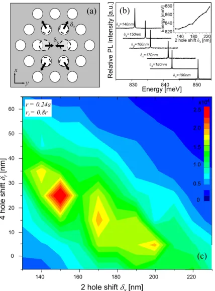
Greater enhancements in the◗-value can be achieved by increasing the parameter space of the modification to the defect geometry. These more extensive modifications [92] have been applied to optimize the①-dipole mode of the sin-gle missing hole defect cavity. As shown in Fig. 15a, two extra holes are added on the①-axis and shifted inwards by ✍①. The radii of four nearest-neighbour holes are reduced by 20% and their lattice sites are shifted radially outwards by✍r. A contour plot of the◗-values in this two parameter optimization is shown in Fig. 15c. Note that the local
max-ima in the figure are not real maxmax-ima, but rather, a result of discretization. The◗-values were extracted from the PL spectra of a series of cavities having different✍①and✍r. From Fig. 15c, there is a broad range of structural param-eters for which the◗-value exceeds 10,000, sufficient for the realization of efficient devices.
Modifications to the defect geometry will affect the resonance energy of the mode as well. The resonance shift as a function of✍①is shown in the inset of Fig. 15b and spans 50 meV for the range of structures investigated. Of this 50 meV, a range of resonant energies spanning 20 meV corresponds to cavities for which◗ exceeds 10,000. High ◗-value cavities covering a range of resonance energies are relevant in regard to tuning the cavity into resonance with the dot emission, in this case, simply by adjusting the position of two holes.
The optimized structure in Fig. 15c possesses a mea-sured◗-value of 28,000, limited by the spectrometer reso-lution. A FDTD simulation of this mode predicts◗=81,000. Such a high◗-value would push a coupled dot-cavity sys-tem into the strong coupling regime [22, 93–95], where spontaneous emission is a reversible process such that the
emitted photon could be reabsorbed by the dot before escap-ing the cavity. The system thus undergoes Rabi oscillations, allowing for the coherent transfer of quantum information between the photon and quantum dot. Such deterministic single photon sources have been demonstrated in coupled atom-cavity systems [96, 97] and allows for a more general quantum computation scheme [98] as compared to those based solely on flying qubits [99].
Given a high◗❂❱ cavity whose resonance energy can be tailored to a known quantum dot transition, one can ad-dress the issue of spatial alignment. This entails combining directed self-assembly with cavity fabrication and requires use of alignment marks etched into the substrate and an ad-ditional planarization growth. The pyramidal nanotemplate growth is carried out as before, except now, the pyramids are precisely positioned with respect to the alignment marks. The sample is repatterned to open large squares around the pyramid. The squares must be sufficiently large to accom-modate a photonic crystal cavity of sufficient size so that the◗-value is limited by vertical losses, typically 10 rings of holes [100]. A second patterned-substrate growth pla-narizes the pyramids through selective InP growth in these large openings. The photonic crystal defect cavities are fab-ricated in the planarized areas using alignment marks to precisely position the defect at the location of the pyramid.
The ultimate goal is a single quantum dot device and the envisioned process entails optical measurements prior to cavity fabrication to identify the emission energy of the dot so that the cavity design can be tailored to the dot. At this stage of development, the primary interest is in the ability to align the dot to the cavity. As such, the necessity for precise spectral alignment is eliminated through the use of a pyramidal nanotemplate having a top (001) apex of 100✂ 100 nm2. This is sufficiently large to support several dots
(see inset, Fig. 16c) and thus act as a broadband internal source, and at the same time sufficiently small to verify spatial alignment.
Fig. 16a shows the ebeam resist pattern on a test pyra-mid that has not been planarized so that the alignment can be verified. We note that the pyramid was exposed during the planarization growth of the other pyramids on the sam-ple. As a result, it has developed some asymmetry that is typical of overgrown pyramids where significant growth has occurred on the❢✶✶✵❣ sidewalls with concomitant de-velopment of nonequivalent❢✶✶✶❣ facets. Nonetheless, the tip of the completed pyramid can be seen roughly posi-tioned between the two①-axis holes, which corresponds to the central antinode of the①-dipole mode of the cavity, shown in Fig. 16b. The emission from a cavity fabricated on a planarized pyramid is shown in Fig. 16c and the very fact that emission is observed is indicative of successful spatial matching. Emission from a reference cavity employ-ing a randomly nucleated dot ensemble as an internal light source is also shown in Fig. 16c, and has been offset along the② axis for clarity of presentation. The lower resonance energy and◗-value of the pyramid-based cavity is a conse-quence of a less than nominal membrane thickness. Such errors should be expected from the complicated fabrication
(b) y x (a) 760 780 800 820 840 planar ensemble site-selected ensemble PL I n te nsity [a.u.] Energy [meV] (c)
Figure 16 (online color at: www.lpr-journal.org) (a) An SEM image of the ebeam resist pattern on an unplanarized completed pyramid. (b) FDTD electric field profile of the①-dipole mode of the cavity. (c) PL spectra from a cavity with site-selected InAs dots as an internal source and with a dot ensemble internal source. The inset shows a pyramidal nanotemplate supporting several dots.
process and can be dealt with using the fine tuning methods mentioned earlier. For example, the cavity resonance can by blue-shifted to the target energy through successive cycles of native oxide removal from the InP membrane [82].
5. Outlook
Progress on quantum dot-based nonclassical light sources has been extremely fast-paced in the last half decade, es-pecially in the area of cavity performance. The key perfor-mance measures for microcavities will continue to improve with advances in design and fabrication, paving the way for deterministic non-classical sources operating in the strong coupling regime. The reliability of dot-cavity coupling, however, must be addressed. The aim of the current review is to highlight the accelerating advances being made in this area. Further advances in the directed self-assembly process should result in consistent single dot nucleation to the point where the electronic properties of the dot can be tuned by virtue of the nanotemplate geometry.
With respect to gated nanotemplate structures, more versatile surface gating techniques will permit a single dot to be subjected to both vertical fields, for charge state con-trol, and lateral fields, for manipulation of the biexciton binding energy. Applying gates to dot-cavity structures
will allow for deterministic loading of a selected dot level, which, in principle, can be used as a gate-driven source of indistinguishable single photons.
Acknowledgements The authors would like to acknowledge the financial support of the Canadian Institute for Advanced Research, the Canadian Institute for Photonic Innovations, QuantumWorks, the Natural Sciences and Engineering Research Council and the Business Development Bank of Canada.
Dan Dalacu received the B. Sc. de-gree in physics from McMaster Uni-versity, Hamilton, Ontario in 1993, the M. Sc. degree in physics from Wa-terloo University, WaWa-terloo, Ontario, Canada in 1996 and the Ph. D. de-gree in physics from Universit´e de Montr´eal, Montr´eal, Qu´ebec in 2000. Since then he has been at the Na-tional Research Council of Canada in Ottawa with inter-ests in quantum dot-based optical devices.
Michael Reimer received his B. Sc. in Honours Physics (Co-operative program) at the University of Wa-terloo in 2000. From 2000–2002 he worked at JDS Uniphase as a Test En-gineer in optical switches for the Re-search and Development Team. He then moved to the Technical Uni-versity of Munich where he com-pleted a M. Sc. in Engineering Physics (coupled quan-tum dots) in 2004. Currently, Michael is completing his Ph. D. in Physics (gated individual quantum dots) through the University of Ottawa and under the su-pervision of Dr. Robin Williams at the National Re-search Council of Canada. He will then undertake a Post-doctoral Fellowship at the Technical University of Delft in The Netherlands where he will investigate quan-tum opto-electronics of a single quanquan-tum dot embedded in a nanowire.
Simon Fr´ed´erick received his B. Sc. and M. Sc. from Universit´e Laval, Qu´ebec city, Canada in 2003 and a Ph. D. degree from the University of Ottawa in 2008. Since then he is com-pleting a post-doctoral fellowship in the Walter Schottky Institute at the Technische Universit¨at M¨unchen, Germany thanks to the Alexander von Humboldt Foundation. His current research inter-ests include semiconductor nanostructures spectroscopy and their interactions with surface plasmon polariton states of metallic nanowires.
Danny Kim received his Ph. D. from the University of Toronto, Toronto, Ontario, Canada in 2007 and is cur-rently at the Naval Research Laboratory in Washington, DC, USA an a post-doctoral fellowship.
Jean Lapointe received his B. Sc. in physics from Laval University in 1984 and his Ph. D. in physics from SUNY Stony Brook in 1993. He joined the Institute for Microstruc-tural Sciences at the National Re-search Council in Ottawa, Canada in 1998 as a member of the nanofabrica-tion group. He was previously with the electrical standards group at the Institute for National Measurements Standards. His current research interests involve the fabrication of semiconductor-based micro and nanostructures using electron beam lithography and other semiconductor processing techniques.
Philip Poole is Group Leader of the Epitaxy Group at IMS-NRC in Ot-tawa. His research interests are in the areas of epitaxial growth of InP-based quantum dot structures for op-toelectronic devices that can take ad-vantage of the novel properties of quantum dots, such as multiwave-length and femtosecond modelocked lasers, and the use of selective area epitaxy to control the nucleation site of individual quantum dots for quantum information studies. Dr. Poole has 12 years of experi-ence at the NRC in the growth of III-V based materials using Chemical Beam Epitaxy.
Geof Aers received the B. Sc. degree in applied physics and the Ph. D. de-gree in theoretical physics from the University of Salford, Salford, UK, in 1974 and 1977, respectively. His primary research topic was surface plasmons. He held a NATO Postdoc-toral Research Fellowship at the The-oretical Physics Institute, University of Alberta, Canada, from 1977 to 1979 researching in surface plasmons and the properties of thin metal films. From 1979 to 1981, he was a Senior Research Associate in the Theory and Computational Science Division of the SERC Daresbury Laboratory, UK, responsible for an interuniversity collaboration on surface science cal-culations. In 1982, he joined the Physics Division of the National Research Council of Canada. He is cur-rently a Principal Research Officer with the Institute for Microstructural Science at the National Research Coun-cil (NRC) of Canada in Ottawa with research interests primarily in nanooptics and nanoelectronics.
Robin Williams received his B. A. in Physics and Theoretical Physics from the University of Cambridge in 1984 and his Ph. D. from the Univer-sity of London in 1988, specializing in Quantum Transport studies of low dimensional Systems. Since 1996 he has been a Research Officer with the Institute for Microstructural Sciences of the Canadian National Research Council, with inter-ests in the growth and optical properties of III-V semi-conductor materials.
W. Ross McKinnon received the B. Sc. and M. Sc. degrees in physics from Dalhousie University, Halifax, NS, Canada, in 1975 and 1976, re-spectively, and the Ph. D. degree in physics from the University of British Columbia, Vancouver, BC, Canada, in 1980. Since then he has been at the National Research Coun-cil of Canada in Ottawa, where he has worked on lithium ion batteries, high-temperature superconductors, InP-based transistors, and most recently biosensors.
Marek Korkusi´nski received his Ph. D. at the University of Ottawa, Canada, in 2004. He completed his postdoctoral fellowships at Purdue University and the National Research Council of Canada and became a per-manent staff member at the NRC In-stitute for Microstructural Sciences in 2005. Dr. Korkusi´nski’s interests include theory of correlated electron and electron-hole systems, and his main research focus is on theory of optical and electronic properties of both self-assembled and gated quantum dots.
Pawel Hawrylak is Principal Re-search Officer and Leader of the Quantum Theory Group at the In-stitute for Microstructural Sciences (IMS). His interests are focused on theoretical and computational NanoScience, and in particular on the electronic and optical properties of correlated electrons in semicon-ductor nanostructures. Dr. Hawrylak is a Fellow of the American Physical Society, Canadian Institute for Ad-vanced Research, and the Royal Society of Canada. He is a recipient of the Humboldt Research Award, CAP Brockhouse Medal and NRC Outstanding Re-search Award.
References
[1] P. Michler, Topics Appl. Phys. 90, 315 (2003).
[2] I. N. Stranski and L. von Krastanow, Akad. Wiss. Lit. Mainz Math.-Naturwiss K1. IIb 146, 797 (1939).
[3] P. M. Petroff, Topics Appl. Phys. 90, 1 (2003).
[4] R. P. Mirin, J. P. Ibbetson, K. Nishi, A. C. Gossard, and J. E. Bowers, Appl. Phys. Lett. 67, 3795 (1995).
[5] P. J. Poole, J. McCaffrey, R. L.Williams, J. Lefebvre, and D. Chitrani, J. Vac. Sci. Technol. B 19(4), 1467 (2001). [6] N. Carlsson, T. Junno, L. Montelius, M. E. Pistol,
L. Samuelson, and W. Seifert, J. Crystal Growth 191, 347 (1998).
[7] H. Folliot, S. Loualiche, B. Lambert, V. Drouot, and A. L. Corre, Phys. Rev. B 58, 10700 (1998).
[8] P. Hawrylak and M. Korkusi´nski, Nonlinear Optics 29, 329 (2002).
[9] A. J. Shields, Nat. Photonics 1, 215 (2007).
[10] P. Michler, A. Kiraz, C. Becher, W. V. Schoenfeld, L. Zhang, E. Hu, and A. Imamogl˘u, Science 290, 2282 (2000). [11] C. Santori, M. Pelton, G. Solomon, Y. Dale, and Y.
Ya-mamoto, Phys. Rev. Lett. 86(8), 1502 (2001).
[12] C. Becher, A. Kiraz, P. Michler, A. Imamogl˘u, W. V. Schoenfeld, P. M. Petroff, L. Zhang, and E. Hu, Phys. Rev. B 63, 121312 (2001).
[13] V. Zwiller, H. Blom, P. Jonsson, N. Panev, S. Jeppesen, T. Tsegaye, E. Goobar, M. E. Pistol, L. Samuelson, and G. Bj¨ork, Appl. Phys. Lett. 78(17), 2476 (2001).
[14] E. Moreau, J. M. G´erard, I. Bram, L. Manin, and V. Thierry-Mieg, Appl. Phys. Lett. 79(18), 2865 (2001).
[15] T. Miyazawa, K. Takemoto, Y. Sakuma, S. Hirose, T. Usuki, N. Yokoyama, M. Takatsu, and Y. Arakawa, J. J. Appl. Phys. 44, L620 (2005).
[16] K. J. Vahala, Nature 424, 839 (2003).
[17] J. M. G´erard, Topics Appl. Phys. 90, 269 (2003). [18] E. Yablonovitch, Phys. Rev. Lett. 58, 2059 (1987). [19] D. Englund, D. Fattal, E. Waks, G. Solomon, B. Zhang,
T. Nakaoka, Y. Arakawa, Y. Yamamoto, and J. J. Vuˇckovi´c, Phys. Rev. Lett. 95, 013904 (2005).
[20] W. H. Chang, W. Y. Chen, H. S. Chang, T. P. Hsieh, J. I. Chyi, and T. M. Hsu, Phys. Rev. Lett. 96, 117401 (2006).
[21] A. Badolato, K. Hennessy, M. Atat¨ure, J. Dreiser, E. Hu, P. M. Petroff, and A. Imamogl˘u, Science 308, 1158 (2005). [22] K. Hennessy, A. Badolato, M. Winger, D. Gerace, M. Atat¨ure, S. Gulde, S. F¨alt, E. L. Hu, and A. Imamogl˘u, Nature 445, 896 (2007).
[23] K. H. Lee, A. M. Green, R. A. Taylor, D. N. Sharp, J. Scrim-geour, O. M. Roche, J. H. Na, A. F. Jarjour, A. J. Turberfield, F. S. F. Brossard, D. A. Williams, and G. A. D. Briggs, Appl. Phys. Lett. 88, 193106 (2006).
[24] T. I. Kamins, and R. S. Williams, Appl. Phys. Lett. 71, 1201 (1997).
[25] R. Tsui, R. Zhang, K. Shiralagi, and H. Goronkin, Appl. Phys. Lett. 71, 3254 (1997).
[26] T. Umeda, K. Kumakura, J. Motohisa, and T. Fukui, Phys-ica E 2, 714 (1998).
[27] R. Williams, G. Aers, P. Poole, J. Lefebvre, D. Chithrani, and B. Lamontagne, J. Crystal Growth 223, 321 (2001). [28] D. L. Huffaker, C. P. Hains, N. Nuntawong, Y. C. Xin,
P. S. Wong, L. Xue, S. R. L. Brueck, and L. Lester, J. Appl. Phys. 99, 033503 (2006).
[29] J. M. Benoit, L. L. Gratiet, G. Beaudoin, Michon, G. Saint-Girons, R. Kuszelewicz, and I. Sagnes, Appl. Phys. Lett. 88, 041113 (2006).
[30] T. Ujihara, Y. Yoshida, W. S. Lee, and Y. Takeda, Appl. Phys. Lett. 89, 083110 (2006).
[31] T. P. Hsieh and J. I. Chyi, Appl. Phys. Lett. 90, 073105 (2007).
[32] M. H. Baier, E. Pelucchi, E. Kapon, S. Varoutsis, M. Gallart, I. Robert-Philip, and I. Abram, Appl. Phys. Lett. 84, 648 (2004).
[33] H. Z. Song, T. Usuki, S. Hirose, K. Takemoto, Y. Nakata, N. Yokoyama, and Y. Sakuma, Appl. Phys. Lett. 86, 113 (2005).
[34] S. Kiravittaya, A. Rastelli, and O. G. Schmidt, Appl. Phys. Lett. 87, 243112 (2005).
[35] Lateral Alignment of Epitaxial Quantum Dots, edited by O. Schmidt (Springer, Berlin, 2007).
[36] D. Chithrani, R. L. Williams, J. Lefebvre, P. J. Poole, and G. C. Aers, Appl. Phys. Lett. 84(6), 978 (2004).
[37] C. Schneider, M. Strauß, T. S¨unner, A. Huggenberger, D. Wiener, S. Reitzenstein, M. Kamp, S. H¨ofling, and A. Forchel, Appl. Phys. Lett. 92, 183101 (2008). [38] Z. G. Xie, and G. S. Solomon, Appl. Phys. Lett. 87, 093106
(2005).
[39] T. S¨unner, C. Schneider, M. Strauß, A. Huggenberger, D. Wiener, S. H¨ofling, M. Kamp, and A. Forchel, Optics Lett. 33, 1759 (2008).
[40] P. Gallo, M. Fellici, K. A. Atlasov, K. F. Karlsson, A. Rudra, A. Mohan, B. Biasiol, L. Sorba, and E. Kapon, Appl. Phys. Lett. 92, 263101 (2008).
[41] M. E. Reimer, D. Dalacu, J. Lapointe, P. J. Poole, D. Kim, G. C. Aers, W. R. McKinnon, and R. L. Williams, Appl. Phys. Lett. 94, 011108 (2009).
[42] R. J. Warburton, C. Sch¨aflein, D. Haft, F. Bickel, A. Lorke, K. Karrai, J. M. Garcia, W. Schoenfeld, and P. M. Petroff, Nature 405, 926 (2000).
[43] K. Kowalik, O. Krebs, S. L. A. Lemlˆaitre, P. Senellart, P. Voisin, and J. A. Gaj, Appl. Phys. Lett. 86, 041907 (2005).
[44] B. D. Gerardot, S. Seidl, P. A. Dalgarno, R. J. Warburton, D. Granados, J. M. Garcia, K. Kowalik, O. Krebs, K. Karrai, A. Badolato, and P. M. Petroff, Appl. Phys. Lett. 90, 041101 (2007).
[45] J. Lefebvre, P. J. Poole, J. Fraser, G. C. Aers, D. Chithrani, and R. L. Williams, J. Crystal Growth 234, 391 (2002). [46] P. J. Poole, G. C. Aers, A. Kam, D. Dalacu, S. Studenikin,
and R. L. Williams, J. Crystal Growth. 310, 1069 (2008). [47] C. Santori, D. Fattal, M. Pelton, G. S. Solomon, and Y.
Ya-mamoto, Phys. Rev. B 66, 045308 (2002).
[48] M. Bayer, G. Ortner, O. Stern, A. Kuther, A. A. Gor-bunov, A. Forchel, P. Hawrylak, S. Fafard, K. Hinzer, T. L. Reinecke, S. N. Walck, J. P. Reithmaier, F. Klopf, and F. Sch¨afer, Phys. Rev. B 65, 195315 (2002).
[49] W. Sheng and P. Hawrylak, Phys. Rev. B 75, 035326 (2005). [50] R. Seguin, A. Schliwa, S. Rodt, K. P¨otchke, U. W. Pohl,
and D. Bimberg, Phys. Rev. Lett. 95, 257402 (2005). [51] R. J. Young, R. M. Stevenson, A. J. Shields, P. Atkinson,
K. Cooper, D. A. Ritchie, K. M. Groom, A. I. Tartakovskii, and M. S. Skolnick, Phys. Rev. B 72, 113305 (2005). [52] A. Greilich, M. Schwap, T. Berstermann, T. Auer, R.
Oul-ton, D. R. Yakovlev, M. Bayer, V. Stavarache, D. Reuter, and A. Wieck, Phys. Rev. B 73, 045323 (2006).
[53] N. Chauvin, B. Salem, G. Bremond, G. Guillot, C. Bru-Chevallier, and M. Gendry, J. Appl. Phys. 100, 073702 (2006).
[54] P. Hawrylak, Phys. Rev. B 60, 5597 (1999).
[55] D. Kim, H. Lefebvre, J. Lapointe, M. E. Reimer, J. Mckee, P. J. Poole, and R. L. Williams, phys. stat. sol. c 3, 3840 (2006).
[56] J. J. Finley, A. D. Ashmore, A. Lemaˆıtre, D. J. Mowbray, M. S. Skolnick, I. E. I. P. A. Maksym, M. Hopkinson, and T. F. Krauss, Phys. Rev. B 63, 073307 (2001).
[57] B. T. Miller, W. Hansen, S. Manus, R. J. Luyken, A. Lorke, J. P. Kotthaus, S. Huant, G. Medeiros-Ribeiro, and P. M. Petroff, Phys. Rev. B 60, 6764 (1997).
[58] F. Findeis, M. Baier, A. Zenner, M. Bichler, Abstreiter, U. Hohenester, and E. Molinari, Phys. Rev. B 63, 121309 (2001).
[59] M. Baier, F. Findeis, A. Zrenner, M. Bichler, and G. Ab-streiter, Phys. Rev. B 64, 195326 (2001).
[60] J. J. Finley, M. Sabathil, P. Vogl, G. Abstreiter, R. Oul-ton, A. I. Tartakovskii, D. J. Mowbray, M. S. Skolnick, S. L. Liew, A. G. Cullis, and M. Hopkinson, Phys. Rev. B 70, 201308(R) (2004).
[61] M. Ediger, G. Bester, A. Badolato, P. M. Petroff, K. Karrai, A. Zunger, and R. J. Warburton, Nat. Phys. 3, 774 (2007). [62] R. J. Young, S. J. Dewhurst, R. M. Stevenson, A. J. Shields,
P. Atkinson, K. Cooper, and D. A. Ritchie, Appl. Phys. Lett. 91, 011114 (2007).
[63] M. E. Reimer, W. R. McKinnon, J. Lapointe, P. J. Poole, G. C. Aers, D. Kim, M. Korkusi´nski, P. Hawrylak, and R. L. Williams, Physica E 40, 1790 (2008).
[64] A. Wojs and P. Hawrylak, Phys. Rev. B 55, 13066 (1997). [65] D. A. B. Miller, D. S. Chemla, T. C. Damen, A. C. Gossard,
W. Wiegmann, T. H. Wood, and C. A. Burrus, Phys. Rev. B 32, 1043 (1985).
[66] P. W. Fry, I. E. Itskevich, D. J. Mowbray, M. S. Skolnick, J. J. Finley, J. A. Barker, E. P. O’Reilly, L. R. Wilson, I. A. Larkin, P. A. Maksym, M. Hopkinson, M. Al-Khafaji, J. P. R. David, A. G. Cullis, G. Hill, and J. C. Clark, Phys. Rev. Lett. 84, 733 (2000).
[67] M. E. Reimer, D. Dalacu, J. Lapointe, P. J. Poole, G. C. Aers, W. R. McKinnon, and R. L. Williams, phys. stat. sol. b 246, 828 (2009).
[68] J. A. Barker and E. P. O’Reilly, Phys. Rev. B 61, 13840 (2000).
[69] O. Benson, C. Santori, M. Pelton, and Y. Yamamoto, Phys. Rev. Lett. 84, 2513 (2000).
[70] R. M. Stevenson, R. J. Young, P. Atkinson, K. Cooper, D. A. Ritchie, and A. J. Shields, Nature 439, 197 (2006). [71] N. Akopian, N. H. Lindner, E. Poem, Y. Berlatzky, J. Avron,
and D. Gershoni, Phys. Rev. Lett. 96, 130501 (2006). [72] S. Seidl, M. Kroner, A. H¨ogele, K. Karrai, R. Warburton,
A. Badolato, and P. M. Petroff, Appl. Phys. Lett. 88, 203113 (2006).
[73] M. E. Reimer, M. Korkusi´nski, D. Dalacu, J. Lefebvre, J. Lapointe, P. J. Poole, G. C. Aers, W. R. McKinnon, P. Hawrylak, and R. L. Williams, Phys. Rev. B 78, 195301 (2008).
[74] M. E. Reimer, M. Korkusi´nski, D. Dalacu, J. Lefeb-vre, J. Lapointe, P. J. Poole, G. C. Aers, W. R. McKin-non, P. Hawrylak, and R. L. Williams, arXiv:0706.1075v1 [quant-ph].


![Figure 13 SEM images of different types of microcavities: (a) mi- mi-cropillar [77], (b) microdisk, and (c) photonic crystal defect cav-ity [78]](https://thumb-eu.123doks.com/thumbv2/123doknet/14150995.471788/13.892.89.371.97.497/figure-images-different-microcavities-cropillar-microdisk-photonic-crystal.webp)