HAL Id: hal-01574542
https://hal.archives-ouvertes.fr/hal-01574542
Submitted on 15 Aug 2017
HAL is a multi-disciplinary open access
archive for the deposit and dissemination of
sci-entific research documents, whether they are
pub-lished or not. The documents may come from
teaching and research institutions in France or
abroad, or from public or private research centers.
L’archive ouverte pluridisciplinaire HAL, est
destinée au dépôt et à la diffusion de documents
scientifiques de niveau recherche, publiés ou non,
émanant des établissements d’enseignement et de
recherche français ou étrangers, des laboratoires
publics ou privés.
Data Transmissions at 1.98 µm in cm-long SiGe
Waveguides
Manon Lamy, Christophe Finot, Julien Fatome, Mickael Brun, Pierre Labeye,
Sergio Nicolleti, Adonis Bogris, Dimitris Syvridis, Mohammed Ettabib, David
Richardson, et al.
To cite this version:
Manon Lamy, Christophe Finot, Julien Fatome, Mickael Brun, Pierre Labeye, et al.. Data
Transmis-sions at 1.98 µm in cm-long SiGe Waveguides. 19th International Conference on Transparent Optical
Network (ICTON 2017), Jul 2017, Gérone, Spain. �hal-01574542�
Data Transmissions at 1.98 µm in cm-long SiGe Waveguides
Manon Lamy1, Christophe Finot1, Julien Fatome1, Mickael Brun2, Pierre Labeye2, Sergio Nicolleti2, Adonis Bogris3,4, Dimitris Syvridis3, Mohammed A. Ettabib5,
David J. Richardson5, Periklis Petropoulos5, Kamal Hammani1
1 Laboratoire Interdisciplinaire Carnot de Bourgogne (ICB), UMR 6303 CNRS – Université de Bourgogne Franche-Comté, 9 Avenue Alain Savary, BP 47870, F-21078 Dijon Cedex, France
2
CEA-Leti MINATEC Campus, 17 rue des Martyrs 38054 Grenoble Cedex 9, France 3
Department of Informatics and Telecommunications, National and Kapodistrian University of Athens, Panepistimiopolis, Ilissia, 15784, Athens, Greece
4 Department of Informatics, Technological Educational Institute of Athens, 12210 Egaleo, Athens, Greece 5
Optoelectronics Research Centre, University of Southampton, Highfield, Southampton, SO17 1BJ, UK e-mail: [email protected]
ABSTRACT
We demonstrate an error-free transmission of 10-Gbit/s optical signals along a SiGe waveguide at a wavelength of 1.98 m. Bit error rate measurements confirm the absence of penalty during the transmission through a 2.5-cm long waveguide having a width of 2.2 m.
Keywords: SiGe waveguides, mid-infrared telecommunications. 1. INTRODUCTION
So far, silicon photonics has attracted much attention for applications in the telecommunication C-band. However, more recently, a shift towards middle infrared (Mid-IR) wavelengths has also been proposed [1]. Indeed, further in the Mid-IR, the nonlinear losses decrease drastically and even vanish beyond 2.2 µm, paving the way to a significant improvement of performance.
At the same time, it is now established that the usual spectral band exploited for optical telecommunications is close to reaching saturation, approaching the so-called ‘capacity crunch’ [2]. Therefore, the recent emergence of thulium doped fiber amplifiers (TDFA) has mainly focused the attention on the wavelengths around 2 µm [3]. This trend has stimulated studies of dedicated photonic components such as InP-based modulators [4]-[5] or arrayed waveguide gratings [6]. High bit rate communications over short distances [7] but also over optical links exceeding a hundred meters have already been successfully demonstrated mainly in low-loss hollow core bandgap photonic crystal fibers [8]-[9].
However, high bit-rate transmission at 2 µm into silicon-based waveguides still call for experiments. In this paper, we focus our attention on Silicon Germanium (SiGe) waveguides. Such components have been thoroughly studied in the C-band [10] where their nonlinear properties have been beneficial for ultrafast optical processing [11]-[13]. However, such waveguides are expected to reach even better performance at mid-IR wavelengths [14]-[15]. Even though they have been used to convert a signal from mid-IR to C-band [16], no high bit-rate transmission has been reported so far. Here, we demonstrate, for the first time, an error-free transmission of a 10-Gbit/s on-off keying signal at 1.98 µm in a 2.5-cm long SiGe waveguide.
2. DESIGN AND PROPERTIES OF THE SI-GE WAVEGUIDE
The device consists of several epi-layers of Si1-xGex grown on a Si substrate. First, a 1.4-µm thick SiGe layer
with 20 % germanium concentration (x = 0.2) was grown by reduced pressure chemical vapor deposition (RP-CVD) to control precisely the Germanium concentration and thus preserve uniformity. Then, standard photolithography and deep reactive ion etching were used to form the strips (see Fig. 1a). Finally, the waveguides were encapsulated with a 12-µm Si cladding layer epitaxially grown with the same RP-CVD technique.
In the following, we focus our attention on a 2.2-µm wide strip waveguide with 5-µm wide input and output tapers. The total length of the strip is 2.5 cm given each taper is 0.5 mm long. The refractive index of the SiGe layer is about 3.54 at 1.98 µm [17]-[18] whereas the silicon has an index close to 3.45. This leads to a predominant mode shown in Fig. 1b and being TE0,0 with an effective index of 3.50.
Butt-coupling is implemented to inject and collect the light into the 2.2 µm SiGe waveguide by means of lensed fibers. First-of-all, the experimental spectral transmission of the component has been measured thanks to an amplified spontaneous source (ASE) and is reported in Fig. 1c. The average total fiber-to-fiber losses are close to 26 dB. We can also observe the oscillatory nature of the transmission function. Such a wavelength dependence is attributed to the multimode nature of the waveguide. More precisely, the waveguide is not
single-mode at these wavelengths and can handle two TE single-modes and two TM single-modes with almost identical effective indices.
Figure 1. (a) Sketch of the waveguide before encapsulation (b) Field of the TE fundamental mode for a waveguide design similar to the experiments: the width is 2.2 µm and height 1.4 µm (c) Waveguide coupling efficiency according to the input wavelength. The dashed vertical line indicates the wavelength of our continuous
wave source used in the following setup.
3. EXPERIMENTAL SETUP AT 2 m
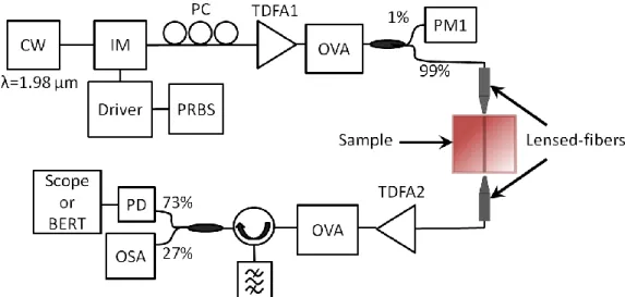
In order to demonstrate the suitability of SiGe waveguides for high speed optical transmissions around 2.0 µm, we have implemented the experimental set-up depicted in Fig. 2. The transmitter is based on a laser diode (CW) centered at a wavelength of 1.98 µm and intensity-modulated by means of a lithium-niobate modulator. The
transmitted signal corresponds to a 231-1 pseudo-random bit sequence (PRBS) at 10 Gbit/s encoded by a
Non-Return-to-Zero On-Off-Keying modulation format. A polarization controller (PC) is inserted after the intensity modulator so as to mitigate the polarization sensitivity of the SiGe waveguide. Two optical variable attenuators (OVA) are inserted into the set-up: the first one is used to control the power injected into the device and thus adjust the optical signal–to-noise-ratio (OSNR) at the receiver, whereas the second one preserves a constant power on the photodiode (PD). A power meter and an optical spectrum analyzer (OSA) measure the power before and after the transmission, respectively. Fiber-to-fiber transmission losses of 30 dB are reached at 1.98 µm. The OSA is also used to evaluate the OSNR of the received signal. The PD can be connected either to a high speed sampling oscilloscope or to a bit error rate tester (BERT) in such a way to monitor the output eye diagrams or perform the bit error rate measurements, respectively. For the back-to-back reference configuration, the sample and the lensed fibers are replaced by an equivalent amount of losses induced by the OVA.
Figure 2. Experimental set-up for the 10 Gbit/s optical transmission at 1.98 µm. CW : continuous wave ; IM: intensity modulator ; PC : polarization controller ; TDFA : thulium doped fiber amplifier ; OVA : optical variable attenuator ; PM : power meter ; PRBS : pseudo-random bit sequence ; OSA : optical spectrum analyzer
4. EXPERIMENTAL VALIDATION OF THE 10 GBIT/S TRANSMISSION AT 2 m
Error-free transmissions have been achieved through the 2.5-cm long SiGe waveguide. Fig. 3 illustrates the typical eye diagrams monitored during these experiments. Both eye diagrams recorded in the back-to-back configuration and after transmission into the waveguide appear well open and do not exhibit any visible degradation.
Figure 3. Eye diagrams for (a) back-to-back configuration and (b) SiGe waveguide output.
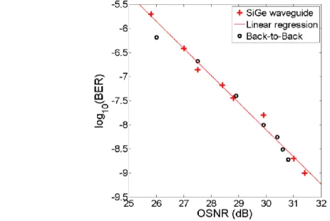
In order to further assess the quality of the transmission, we have performed bit error rate measurements as a function of the OSNR, as summarized in Fig. 4. The results obtained for the back-to-back configuration and for the SiGe waveguide appear very similar and confirm that the transmission through the waveguide does not induce any detrimental distortions. Complementary measurements have demonstrated BER lower than 10-12 (error free).
Figure 4. BER as a function of OSNR for a 2.5-cm long 2.2-m wide SiGe waveguide. The black circles are associated with the back-to-back configuration while red crosses indicate BER measurements at the output of
the waveguide. The red line corresponds to the associated linear regression.
5. CONCLUSIONS
We have shown for the first time to our knowledge, the error free transmission of a 10 Gbit/s optical signal in a 2.5-cm long Silicon Germanium waveguide at a wavelength of 1.98 µm. Despite the fact that the waveguide appears slightly multimode, no significant power penalty has been recorded on the BER measurements. This experimental study confirms that silicon-based integrated photonics is a serious candidate for enabling transmission in the Mid-IR around 2 µm. Moreover, it should be noticed that such SiGe waveguides are more nonlinear in this spectral region than in the C-band [17] therefore, our results call for further studies on nonlinear processing at 2 µm.
ACKNOWLEDGEMENTS
This work was supported by the European Union within the Seventh Framework Programme FP7/2007-2013 under Grant 288304 (STREP CLARITY) and within the framework of the operational Program FEDER-FSE Bourgogne 2014/2020. It was also supported by the Région Bourgogne (Pari Photcom), by the Agence Nationale de la Recherche (Labex Action ANR-11-LABX-0001-01) and by Carnot Arts Institute (PICASSO 2.0 project).
REFERENCES
[1] R. Soref: Group IV Photonics: Enabling 2 µm communications, Nature Photon, vol. 9, pp. 358-359, May 2008.
[2] D.J. Richardson: Filling the Light Pipe, Science, vol. 330, pp.327-328, Oct. 2010.
[3] Z. Li et al.: Thulium-doped fiber amplifier for optical communications at 2 µm, Opt. Express, vol. 21, pp. 9289-9297, Apr. 2013.
[4] M.U. Sadiq et al.: 10 Gb/s InP-based Mach-Zehnder modulator for operation at 2 μm wavelengths, Opt.
Express, vol. 23, pp. 10905-10905, May 2015.
[5] N. Ye et al.: InP-Based Active and Passive Components for Communication Systems at 2 μm. J.
Lightwave Technol., vol. 33, pp. 971-975, Mar. 2015.
[6] H. Zhang et al.:, Dense WDM transmission at 2 μm enabled by an arrayed waveguide grating, Opt. Lett., vol. 40, pp. 3308-3308, Jul. 2015.
[7] K. Xu et al.:, Transmission of IM/DD Signals at 2 µm Wavelength Using PAM and CAP, IEEE Photonics
J. vol. 8, Oct. 2016.
[8] M.N. Petrovich et al.: First Demonstration of 2 µm Data Transmission in a Low-Loss Hollow Core Photonic Bandgap Fiber, in ECOC, Optical Society of America, Amsterdam, 2012, paper Th.3.A.5. [9] M.N. Petrovich et al.: Demonstration of amplified data transmission at 2 µm in a low-loss wide bandwidth
hollow core photonic bandgap fiber, Opt. Express, vol. 21, pp. 28559-28569, Nov. 2013.
[10] K. Hammani et al.: Optical properties of silicon germanium waveguides at telecommunication wavelengths, Opt. Express, vol. 21, pp. 16690-16701, Jul. 2013.
[11] M.A. Ettabib et al.: PSA-based phase regeneration of DPSK signals in a silicon germanium waveguide,
ECOC, 2015.
[12] M.A. Ettabib et al.: All-optical Phase Regeneration with Record PSA Extinction Ratio in a Low-birefringence Silicon Germanium Waveguide, J. Lightwave Technol., vol. 34, pp. 3993-3998, Sep. 2016. [13] M.A. Ettabib et al.: Polarization Insensitive Wavelength Conversion in a Low-Birefringence SiGe
Waveguide, IEEE Photon. Technol. Lett. vol. 28, pp. 1221-1224, Feb. 2016.
[14] M. Brun et al.: Low loss SiGe graded index waveguides for mid-IR applications, Opt. Express, vol. 22, pp. 508-518, 2014.
[15] P. Barritault et al.: Mlines characterization of the refractive index profile of SiGe gradient waveguides at 2.15 µm, Opt. Express, vol. 21, pp. 11506-11515, May 2013.
[16] K. Hammani et al.: Towards nonlinear conversion from mid- to near-infrared wavelengths using Silicon Germanium waveguides, Opt. Express, vol. 22, pp. 9667-9674, Apr. 2014.
[17] N.K. Hon, R. Soref, and B. Jalali: The third-order nonlinear optical coefficients of Si, Ge, and Si1-xGex in the midwave and longwave infrared, J. Appl. Phys., vol. 110, 011301, Jul. 2011.
[18] J. Humlicek et al.: Infrared refractive-index of germanium-silicon alloy crystals, Appl. Opt., vol. 31, pp. 90-94, Jan. 1992.