HAL Id: hal-00272200
https://hal.archives-ouvertes.fr/hal-00272200
Submitted on 14 Apr 2008
HAL is a multi-disciplinary open access
archive for the deposit and dissemination of
sci-entific research documents, whether they are
pub-lished or not. The documents may come from
teaching and research institutions in France or
abroad, or from public or private research centers.
L’archive ouverte pluridisciplinaire HAL, est
destinée au dépôt et à la diffusion de documents
scientifiques de niveau recherche, publiés ou non,
émanant des établissements d’enseignement et de
recherche français ou étrangers, des laboratoires
publics ou privés.
Single Carbon Nanotube Transistor at GHz Frequency
Julien Chaste, Lorentz Lechner, Pascal Morfin, Gwendal Fève, Takis Kontos,
Jean-Marc Berroir, Christian Glattli, Henri Happy, Perti Hakonen, Bernard
Plaçais
To cite this version:
Julien Chaste, Lorentz Lechner, Pascal Morfin, Gwendal Fève, Takis Kontos, et al.. Single Carbon
Nanotube Transistor at GHz Frequency. Nano Letters, American Chemical Society, 2008, 8 (2),
pp.525. �hal-00272200�
J. Chaste, L. Lechner, P. Morfin, G. F`eve, T. Kontos, J.-M. Berroir,1, 2 D.C. Glattli,1, 2, 4 H. Happy,5 P. Hakonen,3 and B. Pla¸cais1, 2, ∗
1Ecole Normale Sup´erieure, Laboratoire Pierre Aigrain, 24 rue Lhomond, 75005 Paris, France 2CNRS UMR8551, Laboratoire associ´e aux universit´es Pierre et Marie Curie et Denis Diderot, France
3Low Temperature Laboratory, Helsinki University of Technology, Otakaari 3A, Espoo, 02015 Finland 4Service de Physique de l’Etat Condens´e, CEA Saclay, F-91191 Gif-sur-Yvette, France
5Institut d’Electronique, de Micro´electronique et de Nanotechnologie,
UMR-CNRS 8520, BP 60069, Avenue Poincar´e, 59652, Villeneuve d’Asq, France (Dated: January 2, 2008)
We report on microwave operation of top-gated single carbon nanotube transistors. From trans-mission measurements in the 0.1–1.6 GHz range we deduce device transconductance gm and
gate-nanotube capacitance Cg of micro- and nanometric devices. A large and frequency-independent
gm∼ 20 µS is observed on short devices which meets best dc results. The capacitance per unit gate
length ∼ 60 aF/µm is typical of top gates on conventional oxide with ǫ ∼ 10. This value is a factor 3–5 below the nanotube quantum capacitance which, according to recent simulations, favors high transit frequencies fT = gm/2πCg. For our smallest devices, we find a large fT ∼ 50 GHz with no
evidence of saturation in length dependence.
PACS numbers:
Carbon nanotube field effect transistors (CNT-FETs) are very attractive as ultimate, quantum limited devices. In particular, ballistic transistors have been predicted to operate in the the sub-THz range [1, 2]. Experimen-tally, a state-of-the-art cut-off frequency of 30 GHz has been reached in a low impedance multi-nanotube device [3], whereas 8 GHz was achieved with a multigate single nanotube transistor [4]. Indirect evidence of microwave operation were also obtained in experiments based on mixing effects or channel conductance measurement in single nanotubes [5–9].
The extraordinary performances of nanotubes as molecular field effect transistors rely on a series of unique properties. High-mobility ”p-doped” single walled nan-otubes can be obtained by CVD-growth, with a semi-conducting gap ∆ ∼ 0.5–1 eV (diameter 1-2 nm) [10]. Low Schottky-barrier contacts, with Pd metallisation, and quasi-ballistic transport result in a channel resistance Rds approaching the quantum limit, h/4e2 = 6.5 kΩ for a 4-mode single walled nanotube [11]. High sat-uration currents, limited by optical phonon emission, allow large biases, Ids ∼ 20 µA at Vds & 1 V in short nanotubes [12, 13]. The above numbers and the good gate coupling explain the large transconductances, gm ∼ Ids/∆ & 10 µS, observed in dc experiments [1]. In the ac, an intrinsic limitation is given by the transit frequency fT = gm/2πCg, where Cgis the gate-nanotube capacitance. Here Cg = CgeoCQ/(Cgeo+ CQ) is the se-ries combination of the quantum and geometrical capac-itances, CQ and Cgeo. Ultrathin oxide coating in CNT-FETs allows to approach the quantum limit with a ca-pacitance per unit gate length lg, Cgeo/lg > CQ/lg =
∗Electronic address: [email protected]
G D S Cgs0 Cds0 Cgd0 Cgd Rgd Cgs Rgs g .Vm gs Rgd
A)
B)
D
S
S
G
G
FIG. 1: Panel A : scanning electron microscope image of a single carbon-nanotube double-gate transistor. Gate length is 300 nm. Panel B : small-signal equivalent circuit of the carbon-nanotube transistor. Extrinsic components are dis-played outside the dashed rectangle. Notations are explained in the text.
4e2/hvF ∼ 400 aF/µm for vF ∼4 × 10⁵ m/s, a typical value for semiconducting NTs [14].
Beside basic interest for quantum limited nano-devices, single nanotube transistors offer new opportunities for fast charge detection due to unique combination of short time response and high charge sensitivity. At present, charge counting experiments performed in nanotube or semiconducting quantum dots use either single electron
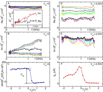
2 0 1 2 -5 0 0 1 2 -5 0 0 1 2 -2 0 0 1 2 0 2 -2 -1 0 1 2 0 4 -2 -1 0 1 2 0 200 0 1 2 0 2 f (GHz) D A E R e ( S a 2 1 ) x 1 0 4 I m ( S a 2 1 ) x 1 0 4 I m ( S P 2 1 ) x 1 0 4 g m ( S ) R e ( S P 2 1 ) x 1 0 4 B V ds =-0.55V F f (GHz) f (GHz) V g (V) V ds =0 C gd C V g (V) d I m [ S P 2 1 ] / 2 Z 0 d ( a F ) Im Re f (GHz) V ds =-0.55V V ds =-0.55V V ds =0 V ds =0 S 0 2 1 x 1 0 3 f (GHz)
FIG. 2: A 3 µm gate transistor. Transmission amplitude S21
as function of frequency. Background contribution (inset of panel A), passive zero-bias (panels A and B) and active bi-ased (panels D,E) contributions. Panels A and D (resp. B and E) have same scales for direct data comparison. Lines correspond to Vg= −2–2V with an increment of 0.4V. Panel
C gives the slope hdℑ[Sp
21(ω)]/dωi as function of gate voltage.
It shows a discontinuity at the opening of channel conduc-tance associated with the gate-drain capaciconduc-tance. Panel F shows device transconductance.
transistors [15, 16] or quantum point contact detectors [17] which operate on microsecond timescales. High sen-sitivity of NT-FET has been demonstrated recently by monitoring tunneling events between the nanotube and a nearby gold particle [18] at the dc limit. Perform-ing such experiments with quantum dots at nanosec-ond timescales would allow to extend charge counting in the coherent regime relevant for full quantum elec-tronics [19]. Given the shot noise limitation of a nan-otube detector of bandwidth 1/τ = 1ns−1, overestimated by the poissonian value pIdsτ /e = 250 electrons for Ids ∼ 10 µA, single charge resolution requires a charge gain gmτ /Cg &250 or equivalently a transit frequency fT = gm/2πCg&40 GHz.
In this letter we demonstrate room-temperature broad-band GHz operation (f = 0.1–1.6 GHz) of nano-transistors made of a single carbon nanotube, with lg = 0.3 µm and 3 µm (channel lengths 1 and 3.5 µm respec-tively). Our main results are the high gm∼10–20 µS in short tubes, and the scaling Cg ∝lg. From the latter we deduce Cg/lg ∼60 aF/µm, in accordance with previous low-frequency determinations [20], and fT ∼50 GHz for our lg= 300 nm devices.
Double-gate carbon nanotube transistors were fabri-cated by e-beam lithography in a coplanar strip-line
ge-0 1 2 -30 0 -2 -1 0 1 0 30 -2 0 2 -10 0 A V g = -1 -1 V [ 0 . 2 V ] g m ( µ S ) R e ( S a 2 1 ) x 1 0 4 B f (GHz) V g (V) V g (V) I d s ( µ A )
FIG. 3: Characterisation of a 300 nm gate transistor. Transmission amplitude of active contribution (panel A) and transconductance (panel B). Inset shows hysteresis in the dc characteristics as Vg is swept.
ometry, with two symmetric top gates (see Fig.1), on oxidized high-resistivity silicon substrates (resistivity 3– 5 kΩ.cm). Nanotubes were synthetized from nano pat-terned catalyst pads using a standard CVD recipe. Pal-ladium contact evaporation is followed by multistep ox-idation of thin aluminium, for a total oxide thickness of ≃6 nm, and finally gold-gate deposition. This process provides full oxidation of Al into Al2O3 with ǫ ≃ 9.8. From sample geometry and dielectric constants, we esti-mate Cgeo/lg∼100 aF/µm.
Devices were characterized in a standard S-parameter measurement using an RF probe station and a network analyzer. Attenuators (−6 dB and −10 dB), followed by bias tees, are mounted directly at the input and out-put ports of the station to minimize standing waves in the Z0 = 50 Ω cables due to large impedance mismatch Rds/Z0 ∼ 300. To compensate for small voltage gain, Z0gm ∼10−3, output signals are amplified by two 0.1– 2 GHz bandwidth low noise amplifiers in series. As a consequence, S-parameter measurement is restricted to the transmission coefficient S21(Vds, Vg), which in turn can be accurately calibrated.
Data reduction and analysis are based on the standard equivalent circuit of Fig.1-B. Extrinsic elements, Cgs0∼ Cds0 ∼10–20 fF, estimated from independent reflection measurements, and Cgd0 ∼ 2 fF measured as explained below, are minimized by the coplanar sample design. The gate capacitance Cg = Cgd + Cgs is splitted into gate-drain Cgd and gate-source Cgs contributions. These are associated to charge relaxation resistances Rgd and Rgs. We have Rgd ≫ 1/Cgdω in the OFF state (Vg & 1 V)
and Rgd≪1/Cgdω in ON state (Vg.0 V). Considering that Z0Cgs0ω ∼ 10−2, Z0Cgd0ω ∼ 10−3 and Z0gm ∼ 10−3 in the low-frequency range ω/2π ≤ 1.6 GHz of our experiment, we obtain S21 = S0 21+ S p 21(Vg) + S a 21(Vds, Vg) with S0 21 ≈ 2Z0ωCgd0 (1) S21p ≈ 2Z0ωCgd/(1 + ωCgdRgd) (2) Sa 21 ≈ −2Z0gm+ ∆S p 21(Vds) (3) being, respectively, the background transmission ampli-tude in the pinched state, the passive contribution at the onset of channel conduction in the zero bias state, and the active contribution under bias. Note that ∆S21p = S21p (Vds) − S21p (0) constitutes the imaginary part of Sa
21. In order to check the validity of our analysis, we first consider the case of long FETs (lg = 3 µm) where gate capacitance contributions are easily resolved. Typical datas are exhibited in Figs.2. The inset of Fig.2.A shows both quadratures of the background transmission S0
21(f ). From the slope of ℑ(S21)(f ) and Eq.(1) we deduce the0 small Cgd0 ∼ 1.5 fF. Substraction of this contribu-tion, keeping zero bias conditions, gives the Vg-dependent passive contribution S21p (f ) shown in (Figs.2.A,B). In the ON state ℑ(S21p ) has a linear frequency dependence, whose slope is plotted in Fig.2-C as a function of Vg. The pinch-off transition appears here as a strong discontinu-ity associated with the divergence of the charge relax-ation resistance Rgd. From the step amplitude and using Eq.(2), we deduce Cgd≃170 aF. This value is very rep-resentative of the five long samples which we have mea-sured with an average of 160 aF and a standard deviation of 50 aF. A small monotonic dependence in ℜ(S21p )(Vg) (Fig.2.A) is also observed which is possibly due to a resid-ual substrate conduction, not taken into account in our analysis.
The active contribution (Figs.2.D-E) is obtained from the bias dependence of S21(f ) at constant Vg. The in-phase signal ℜ(Sa
21)(f ) is prominent and almost fre-quency independent. Slow frequency oscillations are reminiscent of calibration imperfections. Averaging ℜ(Sa
21) over 0.2–1.6 GHz gives, according to Eq.(3), the transconductance as function of Vg shown in Fig.2.F. It has a maximum gm . 3 µS close to the maximum ob-served at the dc ON-OFF transition. Representative values are gm . 1–4 µS. The small negative part, ℑ(Sa
21) ∼ −ℑ(S p
21) in Fig.2.E, is a capacitive contribu-tion due to a shift of the pinch-off under bias. Altogether, these measurements show that one can quantitatively an-alyze the dynamical properties of a single nanotube tran-sistor. With gm ∼1.5µS and Cg ∼85aF (per gate fin-ger), the transit frequency of the 3 µm device of Fig.2 is fT ∼3 GHz.
For short NT-FETs (lg = 300 nm in Fig.1) we ob-serve smaller Cgd and larger gm due to smaller channel resistance. Example shown in Fig.3 represents a new state-of-the-art for RF operation with a maximum of gm(Vg) & 20 µS (double gate fingers). Gate drain
ca-pacitance is Cgd ≃ 35 aF (standard deviation 25 aF). Average values for the six short NT-FETs measured are gm≃12 µS and Cgd ≃35 aF (double gate fingers). As seen on the dc characteristics in the inset of Figs.3.B, hys-teresis is observed in these measurements which has been omitted elsewhere for clarity. Comparing our data for the 300 nm and 3 µm devices shows that, within experimen-tal uncertainty, Cgd scales with lg. Assuming symmetric distribution of gate-drain and gate-source capacitances at zero bias, we obtain Cg/lg≃2Cgd/lg≃60 aF/µm. With gm∼10µS and Cg < 30aF (per gate finger), the transit frequency of the 300 nm device of Fig.3 is fT &50 GHz. These measurements show that NT-FET performances do improve drastically upon gate size reduction down to the nanometric scale (factor of 15 in fT for a factor 10 in size). We now discuss possible routes for improve-ments. First one is to increase gm by reducing access resistance due to the ungated NT sections at drain and source (see Fig.1-A). This effect is significant on devices using deposited CNTs, it is minimized with in situ CVD-grown NTs which are naturally p-doped in the absence of gating. Actually ungated regions are needed to re-duce direct gate-drain/source capacitive coupling. Our values for gate capacitance are close to estimate for the geometrical contribution and in accordance with previ-ous low-frequency measurements in similar top-gated de-vices [20]. They are still smaller than above numbers for the quantum capacitance. One may wonder whether better performance could be achieved by working closer to the quantum limit in using high-κ and/or thinner ox-ides. This would improve gate coupling, but at the same time slow-down electron dynamics due to the screening of electronic interactions as discussed in Ref.[21]. In the ab-sence experimental data and theoretical model, we shall rely on recent numerical simulations showing that transit frequency is maximized for CQ &3–5 × Cgeo [14]. This condition which is close to our experimental realization. The most promising route is further size reduction below 100 nm as we have not observed evidence for saturation down to 300nm. Finally noise performance remain to be characterized, in particular the conditions for shot-noise limited resolution.
In conclusion, we have demonstrated high-transconductance SWNT-FET properties up to 1.6 GHz. We observe that high sensitivity is preserved, and that gate capacitance scales with gate length down to 300 nm. Transit frequencies as high as 50 GHz have been in-ferred, indicating that nanotube FETs are promising fast sensors.
Acknowledgments
Authors acknowledge fruitful discussions with S. Galdin-Retailleau, P. Dollphus, J.P. Bourgoin, V. Derycke, and G. Dambrine. The research has been sup-ported by french ANR under contracts ANR-2005-055-HF-CNT, ANR-05-NANO-010-01-NL-SBPC, and EC
4 STREP project CARDEQ under contract IST-FP6- 011285.
[1] A. Javey, J. Guo, Q. Wang, M. Lunstrom, H. Dai, Nature 424, 654 (2003).
[2] P.J. Burke, Solid-State Electronics 48, 1981 (2004). [3] A. Le Louarn, F. Kapche, J.-M. Berthoux, H. Happy, G.
Dambrinne, V. Derycke, P. Chenevier, N. Izard, M. F. Goffman, J.-P. Bourgoin , Appl. Phys. Lett. 90, 233108 (2007).
[4] PD. Wang, Z. Yu, S. McKernan, J. Burke, IEEE Trans on Nanotechnology 4, 400 (2007).
[5] J. Appenzeller, D.J. Frank, Appl. Phys. Lett. 84, 1771 (2004).
[6] Z. Yu, C. Rutherglen, P.J. Burke, Appl. Phys. Lett. 88, 233115 (2006).
[7] S. Li,Z. Yu, S.-F. Yen, W.C. Tang, P.J. Burke, Nano Letters 4, 753 (2004).
[8] S. Rosenblatt, H. Lin, V. Sazonova, S. Tiwari, and P. L. McEuen, Appl. Phys. Lett. 87, 153111 (2005).
[9] A. A. Pesetski, J. E. Baumgardner, E. Folk, J. X. Przy-bysz, J. D. Adam, and H. Zhang, Appl. Phys. Lett. 88, 113103 (2006).
[10] T. Durkop, S.A. Getty, E. Cobas, M.S. Fuhrer, Nano Letters 4, 35 (2004).
[11] L. Hermann, T. Delattre, P. Morfin, J.-M. Berroir, B. Pla¸cais, D.C. Glattli, T. Kontos, Phys. Rev. Lett. 99, 156804 (2007).
[12] Z. Yao, C. L. Kane, and C. Dekker, Phys. Rev. Lett. 84,
2941 (2000).
[13] B. Bourlon, D.C. Glattli, B. Pla¸cais, J.M. Berroir, L. Forro, A. Bachtold, Phys. Rev. Lett. 92, 026804 (2004) [14] H. Cazin d’Honincthum, S. Baldin-Retailleau,
A. Bournel, P. Dollphus, J.P. Bourgoin, cond-mat/arXiv:0709.3051.
[15] M.J. Biercuk, D.J. Reilly, T.M. Buehler, V.C. Chan, J.M. Chow, R.G. Clark, C.M. Marcus, Phys. Rev. B 73, 201402(R) (2006).
[16] L. Roschier, M. Sillanpaa, W. Taihong, M. Ahlskog, S. Iijima, P. Hakonen, J. Low Temp. Phys. 136, 465 (2004). [17] S. Gustavsson, R. Letrucq, B. Simovic, R. Schleser, T. Ihn, P. Studerus, K. Ensslin, D.C. Driscol, A.C. Gos-sard,Phys. Rev. Lett. 96, 076605 (2006)
[18] A. Gruneis, M.J. Esplandiu, D. Garcia-Sanchez, A. Bach-told, Nano Lett. 7, 3766 (2007).
[19] G. F`eve, A. Mah´e, J.-M. Berroir, T. Kontos, B. Pla¸cais, D.C. Glattli, A. Cavanna, B. Etienne, Y. Jin, Science 316, 1169 (2007).
[20] S. Ilani, L.A.K. Donev, M. Kindermann, P.L. McEuen, Nature Physics 2, 687 (2006).
[21] J. Gabelli, G. F`eve, T. Kontos, J.-M. Berroir, B. Pla¸cais, D.C. Glattli, B. Etienne, Y. Jin, M. B¨uttiker, Phys. Rev. Lett. 98, 166806 (2007).