HAL Id: hal-00931763
https://hal.archives-ouvertes.fr/hal-00931763
Submitted on 1 Jul 2019HAL is a multi-disciplinary open access
archive for the deposit and dissemination of sci-entific research documents, whether they are pub-lished or not. The documents may come from teaching and research institutions in France or abroad, or from public or private research centers.
L’archive ouverte pluridisciplinaire HAL, est destinée au dépôt et à la diffusion de documents scientifiques de niveau recherche, publiés ou non, émanant des établissements d’enseignement et de recherche français ou étrangers, des laboratoires publics ou privés.
Fabrication of a 3GHz oscillator based on
Nano-Carbon-Diamond-film-based guided wave
resonators
Roland Salut, Celine Gesset, Gilles Martin, Badreddine Assouar, Philippe
Bergonzo, Rodolphe Boudot, Omar Elmazria, Sylvain Ballandras
To cite this version:
Roland Salut, Celine Gesset, Gilles Martin, Badreddine Assouar, Philippe Bergonzo, et al.. Fabrication of a 3GHz oscillator based on Nano-Carbon-Diamond-film-based guided wave resonators. Microelec-tronic Engineering, Elsevier, 2013, 112, pp.133 - 138. �10.1016/j.mee.2013.03.096�. �hal-00931763�
Fabrication of a 3 GHz oscillator based
on Nano-Carbon-Diamond-film-based
guided wave resonators
Roland Salut a, Celine Gesset b, Gilles Martin a, Badreddine Assouar c, Philippe Bergonzo b,
Rodolphe Boudot a, Omar Elmazria c, Sylvain Ballandras a
a FEMTO-ST, CNRS-UFC-ENSMM-UTBM UMR 6174, 32 Avenue de l’Observatoire, 25044 Besançon, France
b CEA/LIST/DETECS/SSTM, CEA-Saclay, Bât 451, 91191 Gif-sur-Yvette Cedex, France c IJL, UMR 7198 CNRS-UHP Nancy I, Bd des Aiguillettes, BP 239, 54506 Vandoeuvre les Nancy, France
Abstract
We have investigated the possibility to use carbon-diamond layers exhibiting nano-sized grains for the fabrication of SAW resonators. One of the main purpose was to check the influence of the grain size on the resonator’s spectral signature and to evaluate the fabrication of high frequency sources along this approach. We have investigated various material combinations on Nano-Carbon-Diamond (NCD) layers grown along different techniques (nano-seeding, BEN, followed by MPCVD). The best configuration was based on ZnO/NCD material combination provided the piezoelectric layer was deposited on the so-called nucleation surface of the NCD. Numerous resonators have been fabricated on such substrates, allowing to characterize and exploit the resonance near 3 GHz. An oscillator then was built using such a configuration: its stability has been measured near 10–7 and its phase noise was found near
Keywords
Surface Acoustic Wave, E-beam lithography, Nanocrystalline diamond, RF resonator, Oscillator
1. Introduction
A lot of work has already been dedicated to evaluate the interest of Diamond-Like Carbon (DLC) films for the development of high frequency Surface Acoustic Wave (SAW) devices for various Radio-Frequency (RF) applications [1], [2], [3]. The main interest of such material consists of its very high acoustic phase velocities, typically ranging from 9 to 12 km s−1 when
used as SAW waveguide. The absence of piezoelectric properties of this material however requires the use of a piezoelectric film to excite and detect the waves. As a consequence, the quality of the final device exploiting such material is directly affected by the quality of the piezoelectric layer and the diamond layer as well. Until now, rather modest values of the quality coefficient of SAW resonances on such layered substrate has been reported [4], [5] and only a few studies have been devoted to comprehensively understand the actual limit of these devices and how to overcome the corresponding limitations.
In this work, the possibility to use DLC layers exhibiting nano-sized grains has been investigated for the fabrication of surface acoustic waveguides and more particularly resonators based on such materials. One of the main purposes of this work was to check the influence of the grain size on the quality of the resonator spectral signature and to evaluate the possibility to fabricate high frequency sources along this approach. Considering the results found in the literature [6], [7] and others from a previous work [8], a simple material combination has been considered in that purpose, i.e. Zinc Oxyde (ZnO) deposited using sputtering technique on Nanocrystalline diamond (NCD) layers grown along different techniques based on Microwave Plasma assisted Chemical Vapor Deposition (MPCVD). The different NCD deposition approaches are described and the main characteristics of each material are presented. From all achieved tests, the best identified configuration was based on ZnO/NCD material combination, provided the piezoelectric layer was deposited on the so-called nucleation surface of the NCD. The process consists in growing the NCD layer on a rather thick substrate and then to separate it from its growing support, yielding a self-supported diamond substrate with a high quality surface roughness. Numerous resonators have been fabricated on such substrates, allowing to characterize and exploit resonances near 3 GHz. An oscillator has then been built using such a configuration, but using directly the tip probing conditions instead of dicing and packaging the final device (an operation rather complicated when using self-supported diamond). The stability of the oscillator has been measured near 10−7and its phase noise was found near −100 dBc Hz−1 at 10 kHz. These values are explained
by the fact the resonator was not optimized at first for the exploited mode and operating frequency and the second significant noise contributions were added by the oscillator loop itself. Consequently, large improvements can be expected along the proposed approach. In the first section of the paper we briefly recall the chosen waveguide configuration, showing the dispersion analysis used to design the resonator. We shortly report information about the NCD, the piezoelectric film and the electron beam lithography process. Characterization results of single-port and double-port resonators also are presented. Finally, the fabrication and characterization of the 3 GHz oscillator is described in detail and discussed as a conclusion.
2
. Design of nanocrystalline diamond based saw devices
2.1.
Analysis of dispersion behavior
At first, the typical geometry considered in that work is presented. Although many configurations can be achieved, the simplest one was preferred as an effective implementation of the designed devices was targeted. In that purpose, tricky material combinations requiring numerous etching and/or deposition steps that may prevent the achievement of test vehicles have been avoided. Fig. 1 shows the selected structure and defines axis orientations and layer dimensions.
Fig. 1. Typical waveguide configuration considered for the dispersion analysis. The piezoelectric layer thickness is varied to find the best operating point.
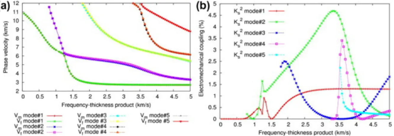
The piezoelectric layer considered to excite and detect the guided waves is C-axis-oriented ZnO. The principal wave parameters have then been computed from the effective permittivity of the material stack top surface. Only non-leaky waves are considered in the present study for reducing as much as possible insertion losses of final devices. Dispersion curves for the selected material configuration are reported in Fig. 2.
Fig. 2. Dispersion curves for the ZnO/Diamond configuration (a) wave velocity and (b) electromechanical coupling.
The most favorable operating point has then been selected considering the following criteria: highest electromechanical coupling (Ks2), mode purity, smallest velocity dispersion (when
possible). The use of mode #3 was expected as the most favorable, with a (frequency) × (thickness) product varying between 1.75 and 2.25 km s−1, leading to a 400 nm
thick ZnO layer to operate near 5 GHz.
2.2. Propagation under periodic grating
Finite Element/Boundary Element Model (the so-called FEA-BIM) have been used to simulate the wave propagation under periodic aluminum grating and to derive mixed matrix parameters to optimize the resonator structures. Particularly, we have studied the evolution of the phase velocity, the electromechanical coupling factor, the reflection coefficient versus the electrode shape along the analysis procedure described in [9]. Contrary to the case of semi-infinite substrate, the actual material stack and targeted working frequency must be considered for
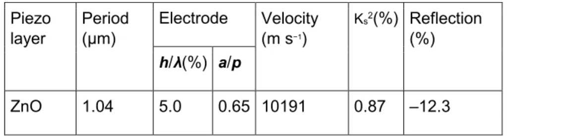
this analysis. Hence, the identified optimal electrode shape is specific to the considered configuration. The electrode relative height and metal ratio are then deduced from the corresponding dispersion curves and reported in Table 1, together with the expected propagation characteristics of the wave.
Piezo layer Period (µm) Electrode Velocity (m s−1) Ks2(%) Reflection (%) h/λ(%) a/p ZnO 1.04 5.0 0.65 10191 0.87 –12.3
Table 1. Mixed matrix parameters vs material configurations, with “h” the thickness of aluminum, “λ” the wavelength, “a” the width and “p” the period of the electrodes.
2.3. Mixed matrix simulation
Both single and double-port devices have been considered for this design step. Fully synchronous devices and structures with a resonant cavity have been simulated. Very optimistic results have been obtained using parameters of Table 1, as reliable information concerning material losses for the diamond and the piezoelectric layers was not accessible. The only important feature here was to adapt the structure to negative reflection mirrors; that is why the cavity is 20.5 µm long (10,25 λ), allowing for the resonance to be located near the center of the stop band. The number of finger pairs in the transducers was set to 40 to favor a maximum signal dynamic. Mirrors are typically composed of 200 electrodes to promote the maximum wave reflection efficiency. The aperture was chosen wide enough to avoid diffraction effects. These patterns were also found compatible with reasonable E-beam process duration.
3. Fabrication of the resonators
The optimized parameters have been considered for the fabrication of resonators operating near 5 GHz. Since material samples were quite small (a few cm2) and the needed resolution
quite high (period 1 µm), the suitable mean to define the electrodes is the Electron Beam Lithography (EBL). In fact, this technique is really dedicated for research [10] and has already been used for that purpose [11]. Typical feature of NCD as well as the Electron Beam Lithography process are briefly describe and some examples of resonators are shown. For each kind of devices (single and double port), we show experimental results.
3.1. Diamond growth on silicon
NCD layer are grown thanks to Microwave Plasma assisted Chemical Vapor Deposition (MPCVD). Three types of gases are exploited, namely Ar, H2 and CH4, and various surface
preparations have been investigated for the preparation of self supported diamond substrates, in order to optimize the seeding conditions.
The process of fabrication is reported in Fig. 4. After cleaning the silicon wafer (roughness = 2 nm RMS), the NCD layer is grown either by BEN (Bias Enhanced Nucleation)-MPCVD [12] where the ion bombardment itself induces the nucleation, or by nanoseeding [13]where the surface is seed with diamond nanoparticles (size 10 nm). As these approaches are slow (200 nm h−1), the substrates are then placed in a standard MPCVD
reactor to obtain a thick layer of polycrystalline diamond (P = 4500 W, P = 100 hPa,
T = 840 °C, %CH4 = 5%, %N2 = 1%, t = 100 h, thickness = 300 µm). Finally, the silicon wafer
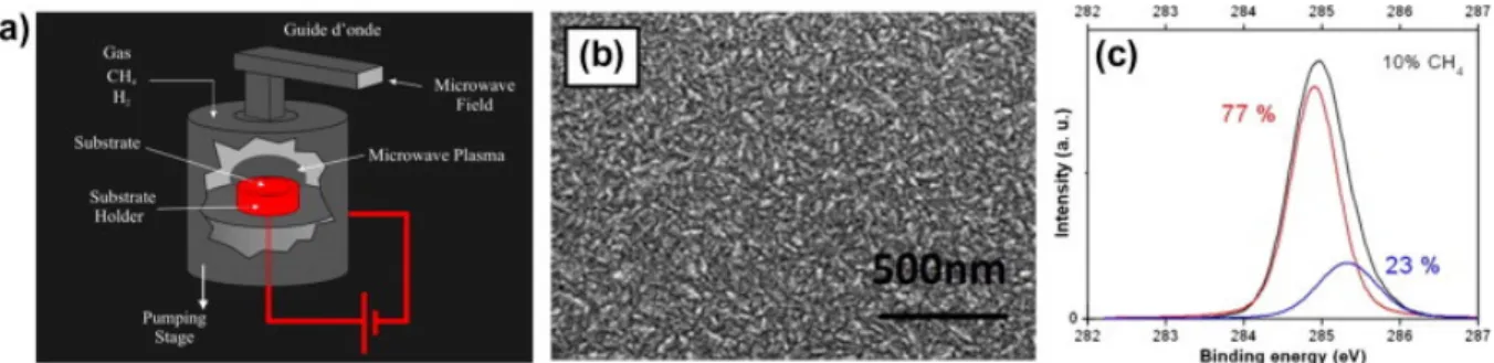
and XPS (Fig. 3c). The XPS spectrum shows a high contribution (77%) of the carbon sp3 (characteristic of the diamond), and only 23% of a less organized phase.
Fig. 3. Nanocrystalline growth – (a) principle of the MPCVD growing chamber, (b) SEM view of a diamond film grown using a 10% CH4 plasma and (c) characterization by XPS.
Fig. 4. Fabrication of self-supported substrate of nanocrystalline diamond – A highly polished substrate of silicon is used, nanocrystalline and polycrystalline diamond layers are then deposited, and the silicon is finally removed thanks to wet etch.
The best result has been obtained with the nanoseeding method compared to the BEN-MPCVD. The RMS roughness of the final diamond substrate is strictly faithful to the initial one, 2 nm.
Finally, the 450 nm thick layer of ZnO is deposited by RF sputtering. A zinc cathode is used, and the process operates at T = 450 °C, P = 100 W and a gas mixture Ar : O2 (1:2).
3.2. E-beam writing technology
Here the implemented E-beam process is described to achieve reliable test vehicles. The main steps are presented on Fig. 5 and listed in this short summary. After cleaning the sample, a 260 nm thick layer of PMMA is deposited on the substrate by centrifugation, and then a conductive layer (15 nm of chromium) is sputtered on the PMMA surface to allow the charge evacuation. The exposure is then performed by means of a Raith e_line system operating at 15 kV and 30 pA. The used clearing dose is 170 µC cm−2. After removing the Cr layer, the
resist is developed in a MIBK:IPA (1:3) bath for 45 s and rinsed in IPA. Finally, aluminum evaporation performed at 1 nm min−1, enables to get a 50 nm thick layer. The sample is then
Fig. 5. EBL process – First, a 260 nm layer of PMMA is spin-coated on the substrate and a layer of chromium is sputtered. Then, the electronic resist is exposed with a 15 keV energy beam and developed. Finally, the 50 nm Aluminum layer is deposited and the substrate is immersed in Acetone for the final step of lift-off.
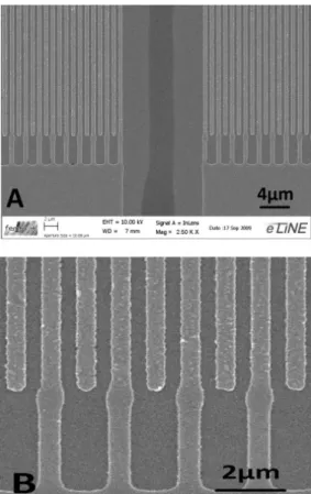
Twenty to thirty resonators are typically built on a given sample, yielding statistical assessment of the device operation. After lift-off, the devices are characterized thanks to a high resolution SEM, and two pictures are presented on Fig. 6.
Fig. 6. SEM pictures of a double port resonator – (A) overview around the cavity and (B) zoom on the fingers.
4. Characterization and integration of the resonators
4.1. Simple and double port resonators
Most fabricated devices have been found free of defects and measured. The first result was obtained with a simple port resonator on a Diamond/ZnO substrate, and is presented on Fig. 7. This kind of configuration shows a good agreement with expectations. The deduced phase velocity is
v
= 10,600 m s−1 and the slope reveals a significant level of loss, which can beattributed to the high roughness of the substrate which leads both to poor definition of the electrodes and propagation loss.
Fig. 7. Experimental admittance for a simple port resonator on a Si/Diamond/ZnO substrate. As the phase rotation was quite small for a single port resonator and the parameters to adjust a negative-resistance-based oscillator hardly achievable in practice, a double port resonator has been implemented with the hope to get rid of these difficulties and to allow the fabrication of a feed-back oscillator, much simpler to achieve. Fig. 8 shows an example of such a device built on a self-supported substrate for which the NCD has been grown using the nanoseeding method. The theory assessment has allowed to point out a ZnO thickness higher than the expected one (500 nm for 400 nm expected). Nevertheless, these results show that the films operate well enough to allow a reliable analysis of the obtained results.
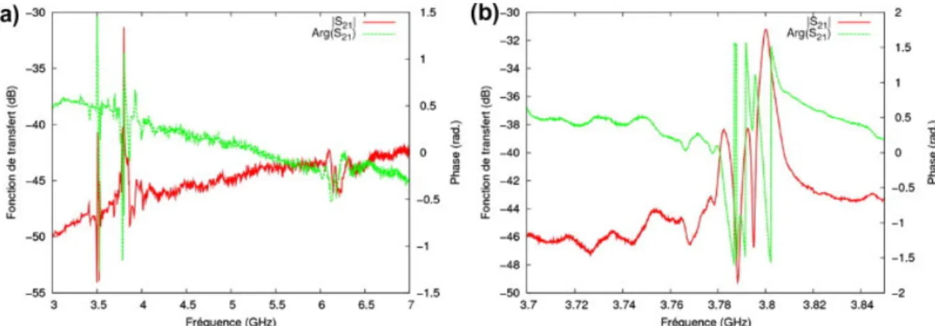
Fig. 8. Example of double-port resonator transfer function (a) wide spectrum and (b) zoom near the first mode #2.
4.2. Integration
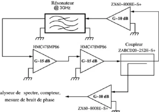
Although the response dynamics remains rather small and the insertion losses notably high (about 28 dB), we decided to build an oscillator stabilized using the end-of-the-stop-band resonance of the second mode. As we did not manage to die the diamond, the connection between the resonator and the phase-locking electronics has been achieved via tip probing, which leads to the use of a cable with a notable length imposing a 45 dB amplification to meet the Barkhausen conditions. Fig. 9 shows the oscillator scheme and the corresponding components nomenclature.
Fig. 9. Scheme of the implemented oscillator.
Fig. 10 shows the phase noise measurement for this oscillator. The typical noise figure at 10 kHz is found near −100 dBc Hz−1. A loaded quality factor Q of the resonator of many
thousands has been deduced from this result whereas experimental characterization provides a value of about one thousand. It seems to indicate the large part of the amplifier loop to the phase noise. One can also evaluate a short term relative stability from this phase noise measurement of 3.10−9 for 1 s. This estimation is achieved considering a continuous 1/f3 slope
until 1 Hz, which appears a bit hypothetic accounting for the thermal sensitivity of the exploited mode (near –40 ppm K−1). One should better keep in mind a value of 10−7 for 1 s experimentally
Fig. 10. (a) Phase noise measurement of the oscillator and (b) short term stability of the oscillator (Allan variance).
5. Conclusion
In this work, high frequency resonators have been developed for frequency source applications. These resonators have been manufactured using Electron Beam Lithography on ZnO/Diamond substrate, exploiting the nucleation side of the NCD exhibiting small arithmetic averaged roughness (2 nm RMS) compatible with a reliable and reproducible lithography step. nanocrystalline diamond films and substrates have also been used to minimize the acoustic losses expected in standard poly-crystal diamond-like carbon films due to large grain overlays [14], expected to favor acoustic diffusion along the surface propagation. Single and double port resonators have been built in the 3–6 GHz frequency range. Double port resonators have been found compatible with the oscillator application, yielding a first oscillator demonstration near 3 GHz. Considering the operation condition of this oscillator, one should improve the corresponding stability characteristics without too much efforts, simply developing an adapted packaging of the resonator and a robust low noise amplifier loop, to reach or to overtake standard characteristics, for instance −90 dBc Hz−1 at 1 kHz and a floor noise of −165 dBc Hz−1
[15].
Acknowledgement
This work is supported by the French Direction Générale de l’Armement (DGA) under Grant #636974 0680238016.
References
[1] O. Elmazria, F. Benedic, M. El Hakiki, H. Moubchir, M.B.Assouar, F.O. Silva. Diamond and Related Materials, 15 (2006), pp. 193-198
[2] A. Hachigo, H. Nakahata, K. Itakura, S. Fujii, S. Shikata. Proc. of the IEEE Ultrasonics Symposium (1999), pp. 325-328
[3] M. Pereira da Cunha, E.L. Adler, D.C. Malocha. Proc. of the IEEE Ultrasonics Symposium, 1 (2000), pp. 283-286
[4] H. Nakahata, et al. Proc. of the IEEE Ultrasonics Symposium (1998), pp. 319-322
[5] S. Fujii, S. Kawano, T. Umeda. Proc. of the IEEE Ultrasonics Symposium (2007), pp. 2367-2370
[6] I.T. Tang, H.J. Chen, W.C. Hwang, Y.C. Wang, M.P.Houng, Y.H. Wang. Journal of crystal growth, 262 (2004), pp. 461-466
[7] W.C. Shih, R.C. Huang. Vacuum, 83 (2008), pp. 675-678
[8] Roland Salut, Céline Gesset, Samuel Saada, VentsislavYantchev, Badreddine Assouar, Fabien Bénédic, PhilippeBergonzo, Frank Omnes, Vincent, Edon, Denis Rémiens, Omar ElMazria, Ilia Kartadjiev. Proc of the IEEE Ultrasonics Symposium (2009), pp. 927-930
[9] S. Ballandras, A. Reinhardt, V. Laude, A. Soufyane, S.Camou, W. Daniau, T. Pastureaud, W. Steichen, R. Lardat, M. Solal, P. Ventura. Journal of Applied Physics, 96 (12) (2004), pp. 7731-7741
[10] L. Pain, S. Tedesco, C. Constancias. Physique, 7 (2006), pp. 910-923
[11] P. Kirsch, M.B. Assouar, O. Elmazria, M. El Hakiki, V.Mortet, P. Alnot. IEEE Transactions on Ultrasonics, Ferroelectrics, and Frequency Control, 54 (7) (2007), pp. 1486-1491
[12] J.C. Arnault, S. Saada, S. Declos, L. Rocha, L. Intiso, R.Polini, A. Hoffman, S. Michaelson, P. Bergonzo. Chemical Vapor Deposition, 14 (7–8) (2008), pp. 187-195
[13] J.C. Arnault, S. Saada, M. Nesladek, O.A. Williams, K.Haenen, P. Bergonzo, E. Osawa.
Diamond and Related Materials, 17 (7–10) (2008), pp. 1143-1149
[14] T. Uemura, S. Fujii, H. Kitabayashi, K. Itakura, A.Hachigo, H. Nakahata, S. Shikata, K. Ishibashi, T. Imai. Japenese Journal of Applied Physics, 41 (2002), pp. 3476-3479
[15] S. Fujii, Y. Takada, H. Harima. Proc. of the Frequency Control Symposium (2005), pp. 499-502