HAL Id: hal-01864468
https://hal.archives-ouvertes.fr/hal-01864468
Submitted on 6 Oct 2019
HAL is a multi-disciplinary open access
archive for the deposit and dissemination of
sci-entific research documents, whether they are
pub-lished or not. The documents may come from
teaching and research institutions in France or
abroad, or from public or private research centers.
L’archive ouverte pluridisciplinaire HAL, est
destinée au dépôt et à la diffusion de documents
scientifiques de niveau recherche, publiés ou non,
émanant des établissements d’enseignement et de
recherche français ou étrangers, des laboratoires
publics ou privés.
Using multifunctional standardized stack as universal
spintronic technology for IoT
Mehdi B. Tahoori, Sarath Mohanachandran Nair, Rajendra Bishnoi, Sophiane
Senni, Jad Mohdad, Frédérick Mailly, Lionel Torres, Pascal Benoit, Abdoulaye
Gamatié, Pascal Nouet, et al.
To cite this version:
Mehdi B. Tahoori, Sarath Mohanachandran Nair, Rajendra Bishnoi, Sophiane Senni, Jad
Mo-hdad, et al.. Using multifunctional standardized stack as universal spintronic technology for IoT.
DATE: Design, Automation and Test in Europe, Mar 2018, Dresden, Germany.
pp.931-936,
�10.23919/DATE.2018.8342143�. �hal-01864468�
l)Karlsruhe Institute ofTechnology, Germany
3) 2)LIRMM, UMR CNRS 5506, University ofMontpellier, France
Univ. Grenoble Alpes, CNRS, CEA, INAC-SPINTEC, F-38000 Grenoble, France
4)Transilvania University ofBrasov,29B-dul Eroilor, 500036 Brasov, Romania
Abstract- For monolithic heterogeneous integration, fast yet low-power processing and storage, and high integration density, the objective of the ED GREAT project is to co-integrate multiple digital and analog functions together within CMOS by adapting the Magnetic Tunneling Junctions (MTJ s) into a single baseline technology enabling logic, memory, and analog functions, particularly for Internet of Things (loT) platforms. This will lead to a unique STT-MTJ cell technology called Multifunctional Standardized Stack (MSS). This paper presents the progress in the project from the technology, compact modeling, process design kit, standard cells, as well as memory and system level design evaluation and exploration. The proposed technology and toolsets are giant leaps towards heterogeneous integrated technology and architectures for loT.
I. INTRODUCTION
Billions of Smart Connected Devices are sold every year with an increase of both the number and complexity for these systems. The interest for developing smart connected systems (Smart Sensors, Secure Elements, etc.) based on an "Internet of
Things" (loT) is growing fast. The number of Internet-connected devices surpassed the number of human beings on the planet in 2011, and by 2020, Internet-connected devices are expected to number between 26 billion and 50 billion. New applications in loT will require storing and computing ever-increasing amounts of data in battery-powered systems. The main components of loT devices are autonomous battery-operated smart embedded systems comprising communication circuits, sensors, computing/processing devices as well as integrated memories. These smart connected devices embed RF circuits for communications, digital circuits for data processing, memory for data storage as well as analog circuits such as sensors, filters, and converters. To reduce the fabrication costs and improve system integration, it is desirable to have all these functionalities on the same die and using the same fabrication technology.
A Non-Volatile Memory (NVM) based technology that would allow realizing digital, RF and analog functions on the same chip could enhance the integration and reduce the cost for the fabrication of high-end embedded platform for smart connected loT systems, push forward their miniaturization, decrease their power consumption (by reducing the power consumptions of memory and sensor interfaces blocks by 5x or lOx), enhance their security and improve their reliability while meeting the high performance requirements.
The Magnetic Tunnel function (MTJ), as the building block of non-volatile magnetic memory (MRAM) such as Spin
Transfer Torque (STT), is a multilayered nanostructure whose
used for memory and/or logic functions ("processing/storing"). The MTJ, however, can also be used as a variable resistance for analog applications, including magnetic field or current sensor ("sensing"). So far, these different functions have been achieved separately, using dedicated optimized magnetic tunnel junction stacks. The idea of the GREAT project is to adapt the STT-MRAM to a single baseline technology allowing performing logic and analog functions in the same SoC. This will lead to a unique STT-MRAM MTJ cell which we call
Multifunctional Standardized Stack (MSS). The basic idea consists in using a standard perpendicular STT-MTJ in memory mode with additional permanent magnets around it, generating an in-plane bias magnetic field to change its behavior for sensors or RF application. This requires only one additional lithography step whose additional cost will be very low compared to the gain offered by the co-integration.
For memory applications, MTJs can have adjustable retention by playing with the diameter of the stack thus allowing to minimize the switching current according to the specified retention. For RF and sensor functions, patterned permanent magnets (for instance made of CoCr alloy or NdFeB) can be added on the two sides of the MTJ pillars, as this is done to bias magnetoresistive heads in hard disk drives. For the spin transfer oscillator, the size and shape of the permanent magnet biasing layer will be adjusted to produce a horizontal field in the order of half of the effective perpendicular anisotropy field (-lkOe) so that the free layer magnetization will be tilted at about 30°. For sensor applications, we will develop a sensor sensitive to the out-of-plane component of the field. First, the diameter of the pillar will be increased compared to the MSS used for memory functions. Besides, the size and shape of the permanent magnet biasing layer will be adjusted to produce a horizontal field slightly larger than the effective perpendicular anisotropy field (-1kOe) so that the free layer magnetization will be pulled in-plane by this biasing field. When submitted to an out-of-in-plane field to be sensed, the free layer magnetization will rotate upwards or downwards producing a resistance change proportional to the out-of-plane field amplitude.
In this paper we focus on the development in the modeling, process design kit, standard cell, memory evaluation and system level analysis in the scope of this European project. We also show how these pieces of the flow can be combined for cross-layer hybrid design and evaluation.
The rest of this paper is organized as follows. The process design kit is explained in Section II. Section III is devoted to variability analysis. Section IV describes the cross-layer
]1.
b
4
3
1e-05 le-10 1'e- 5
RER
2 00 0.s
..,f >. I:n u C':i t:: CDro
0 ...J co:i "0 I:n ctli C\.i Q) a: 0 C\iumbe of corrected bits
o
le-OS 1e- 10 1e-15
WER 0 "=t 0 OJ T"" til 0
.s
~ >-(J 0 c: co Q) ~ 0 ...J CD ~ 0 ~ "=t 0 C\IFig. 8. Effect of ECCs on write latency for WER of 1 x 10-18
technology node (45 nm) as shown by the higher value of (JIll in this node. Furthermore, due to the high value of(J for the latencies, a large timing margin is required to keep the error rates within acceptable limits. However, using a smaller technology node helps with both read and write energy reduction. Fig. 7 presents the overall latencies for different values of input Read Error Rate (RER) and Write Error Rate (WER). It can be seen that for lower values of target error rates, high timing margins are required.
Fig. 7. Overall read and write latencies for various error rates.
Table 1: Overall latency and energy values for 45 nm and 65 nm technology nodes for a memory array of 1024x 1024
Another approach is to reduce the timing margin and employ appropriate Error Correcting Codes (ECCs) to correct errors in the tail of the distribution. The effect of various ECC schemes on the write latency is shown in Fig. 8. The figure shows that compared to the case with no ECC (O-bit correction), there is a drastic improvement in latency by using an ECC with one-bit error correction. However, the improvement in latency for higher bit error correction is comparatively less. 00- 0 S ~ >. 0 u 0 t:: 0 CD Cii CD ..J ~ ~ ~
s:
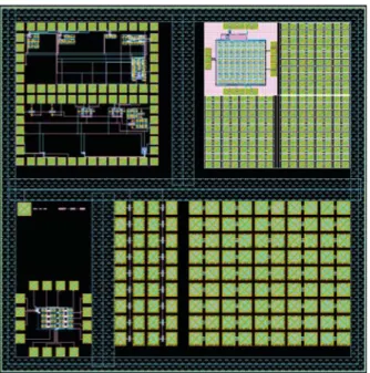
0C\J 45nm 65nm Nominal Jl () Nominal Jl () Write Latency (ns) 4.9 14.7 1.82 4.4 12.1 1.32 Write Energy (pI) 159.0 425.0 3.73 272.8 512.2 2.79 Read Latency (ns) 1.2 1.7 0.08 1.22 1.5 0.05 Read Energy (pI) 3.4 4.8 0.002 4.8 5.7 0.001Fig. 6. Layout of the first demonstrator, embedding test structures and circuits from different partners
feedback using an MSS-based programmable current source, has also been proposed and will be integrated in the SoC.
Some of these IPs as well as test structures have been embedded in a first test chip (Fig. 6) whose testing results will be used as a feedback to prepare the final demonstrator.
III. VARIABILITY ANALYSIS IN STT-MRAM
Like any nano-scale device, STT-MRAM is also affected by manufacturing variations as the technology scales down in the magnetic fabrication process as well as the CMOS process. In addition, the impact of process variation on the magnetic devices exacerbates the stochastic switching behavior of the MTJ. Therefore, quantifying the effect of these variations at the memory architecture level is important for a realistic estimation for the performance, energy and reliability for STT-MRAM. To this end, we have developed a Variation Aware Estimator Tool for STT-MRAM (VAET-STT) [6], an early stage design
exploration tool for STT-MRAM, which considers process variation, stochastic switching and reliability requirements in its analysis and memory configuration optimization.
The VAET-STT tool is built on the top of NVSim [2] and extends it to account for variability in both the bit-cell and peripheral components. The impact of variability causes the latency and energy of the bit-cell and peripherals to follow distributions instead of being a single (nominal) value as shown in Table 1. The table shows the nominal values (variation-unaware values obtained from NVSim) of the latency and energy along with the mean (Il) and standard
deviation (J) of the distributions at two different technology nodes (45 nm and 65 nm).
From Table 1, we see that Il is much higher than the
nominal values. It can also be seen that the effect of variations in write and read latencies is more pronounced in the smaller
Report total performance, total energy and total area System-level configuration such as processor type cache levels, cache-size, etc. Applications based on MiBench & SPEC2000/2006 benchmarks
File Parser- Extract runtime, read/write memory accesses, hit/miss rates & instruction-per-cycle
A. Circuit level
First, a Process Design Kit (PDK) is developed with the device-level parameters, as discussed in Sec. II. This PDK is then used as an input for circuit-level simulation through SPICE. Thus, single bit cells and flip-flops based on MRAM, sense amplifiers, and write circuits can be analyzed. For SPICE simulation, a template file is created for the netlist, stimulus and Measurement Descriptive Language (MDL) after performing several independent simulations. Next, the SPICE simulation generates output measurement file that is then parsed to extract the required cell level parameters such as switching current, delay and energy values. These values are updated into the cell configuration file of the VAET-STT tool.
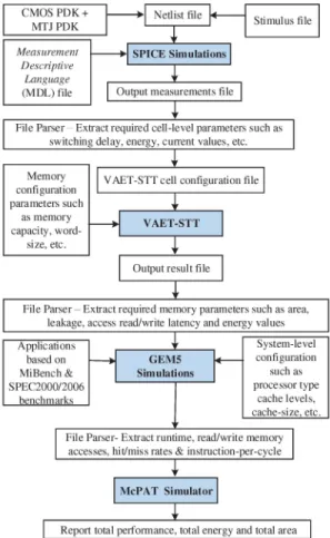
Fig. 10. Hybrid design exploration framework, MAGPIE flow
suite executed on an Exynos 5 Octa SoC model integrating STT-RAM memory at cache level. According to gained insights, MAGPIE improves the productivity by significantly reducing the design exploration.
Memory configuration parameters such as memory capacity, word-size, etc. CMOSPDK+ MTJPDK
File Parser - Extract required cell-level parameters such as switching delay, energy, current values, etc.
File Parser - Extract required memory parameters such as area, leakage, access read/write latency and energy values
Measurement Descriptive
Language
(MDL) file
,Rl;ladJp _rloo (n=:;)
Fig. 9. Read disturb probabilities for different read periods.
IV. CRoss-LAYER HYBRID MEMORY DESIGN EXPLORATION FRAMEWORK
The MAGPIE (Manycore Architecture enerGy and Performance evaluatIon Environment) [8] is a framework with the aim to explore the impact of STT-MRAM on real systems requiring a cross-layer investigation where device, circuit, memory, and system levels are taken into account. Such a simulation platform could be a fast and cost-effective solution to provide essential feedback to enhance the development of STT-MRAM devices. Fig. 10 describes the cross-layer simulation environment for hybrid design exploration.
MAGPIE is built upon three mature and popular tools: the gem5 full-system simulator, the McPAT and VAET-STT power/energy and area estimation tools for CMOS, SOl and emerging non-volatile memory technologies. MAGPIE promotes a script-oriented approach that assists a designer in the design and evaluation tasks.
The MAGPIE evaluation flow considers input parameters comprising information related to the software and hardware components of a target system. The software-related inputs include a gem5 execution script file for each workload/application to be executed, together with the underlying operating system supported by the considered full-system simulator. From the hardware perspective, a number of parameters of the target manycore architectures are required: types and number of cores, memory hierarchy and its technology-specific properties, and the interconnect type.
The VAET-STT tool helps the designer in analyzing the trade-offs between the energy and performance requirements against the target reliability requirements. Moreover, it provides realistic estimations which can better reflect the chip behavior after fabrication. The results show that the variation-aware latency and energy values are significantly higher than those of the nominal case, highlighting the importance of variation-aware analysis.
B. Memory level
Memory-level evaluation is performed thanks to VAET-STT, built on top of NVSIM[3],which is described in Section III. Based on circuit-level data of single bit cell (Section II) and the desired memory architecture information such as capacity, data width, and type of memory (e.g. Cache, RAM, CAM), VAET-STT estimates the access time, the access energy, and the total area of a complete memory chip taking the impact of variations also into account. This tool also includes optimization settings (e.g. buffer design optimization) and various design constraints to facilitate a variation-aware design space exploration before the fabrication of the actual memory chip.
c.
System levelMemory-level information is extracted from the previous step to explore the impact of different memory technologies at system level. An accurate performance simulator (gemS [4])is used to simulate a single-core or a multi-core architecture with its memory hierarchy. GemS generates a detailed report of the system activity including the number of memory transactions (e.g. number of reads/writes, number of hits/misses) and the execution time. This activity information is then used by McPAT [5], a power and area estimator tool at architecture level. Extending the exploration framework with McPAT allows us to analyze not only the energy consumption related to the memory components, but also to evaluate the energy of the complete system including the processor cores, buses, and memory controller.
Fig. 11. Energy breakdown by component when executingbodytrackkernel on big.LITTLE architecture
D. Results
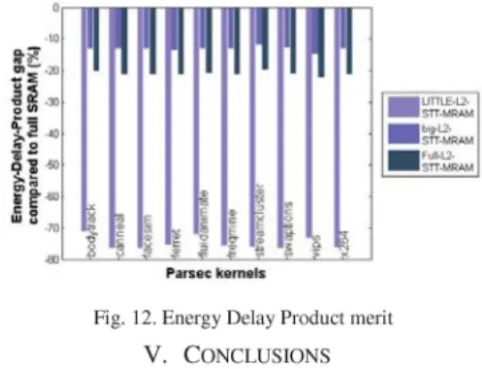
Fig. 11 provides a summary of typical results obtained with MAGPIE. The following evaluation scenarios are considered: big.LITTLE architecture where all cache memories are in SRAM (i.e., our reference scenario, referred to as Full-SRAM); similar architecture but the L2 cache of the LITTLE cluster is now in STT-MRAM (LITTLE-L2-STT-MRAM), similar architecture but the L2 of the big cluster is in STT-MRAM (big-L2-STT-MRAM), and similar architecture where L2 caches of both clusters are in STT-MRAM (Full-L2-STT-MRAM).
Fig. 12 shows for each kernel its execution time, energy and Energy-Delay-Product (EDP), for the LITTLE-L2-STT-MRAM, big-L2-STT-MRAM and Full-L2-STT-MRAM scenarios compared to the Full-SRAM reference scenario. Here, a 45 nm memory technology is used for illustration.
As expected, putting STT-MRAM in the L2 caches can increase the execution time due to its well-known higher write latency compared to SRAM. Only the scenario with STT-MRAM in the L2 cache of the LITTLE cluster reduces the execution time, up to 50% compared to Full-SRAM. Nevertheless, the overall energy consumption is improved in all scenarios, at least up to 17%. The EDP plotted in Fig. 12 is the product between execution time and energy consumption. It shows that the penalty observed on the execution time when introducing STT-MRAM in L2 caches is compensated by the enabled energy savings.
Fig. 12. Energy Delay Product merit V. CONCLUSIONS
In this paper we reviewed the objectives and activities in this European project and presented our preliminary results. This project which spans from technology level all the way to architecture and system, is based on the Multifunctional Standardized Stack (MSS) to enable the use of spintronics for analog and digital sub-systems of loT platforms. This leads to better integration of embedded & mobile communication systems and a significant decrease of their power consumption.
VI. ACKNOWLEDGMENT
This work was supported by the European Union under Horizon-2020 Program as part of the GREAT project (http://www.great-research.eu/) under grant agreement No 687973. We would like to warmly thank people who worked on the technology in the framework of this project at Spintec Laboratory (Ricardo Sousa, Nathalie Lamard, Laurent Vila, Ursula Ebels, Lucian Prejbeanu), at Singulus (Juergen Langer, Jerzy Wrona) and at TowerJazz (Philippe Azoley, Yakov Roizin).
REFERENCES
[1] K.Jabeur, et al. "Comparison of Verilog-A compact modelling strategies
for spintronic devices," Electronics Letters, pp. 1353-1355,2014. [2] L. Barthe, et al. "The secretblaze: A configurable and cost-effective
open-source soft-core processor." IPDPSW, pp. 310-313,2011. [3] X. Dong, et al. "NVSim: A Circuit-Level Performance, Energy, and
Area Model for Emerging Nonvolatile Memory," TCAD, vol. 31, no. 7, pp.994-1007,2012.
[4] N. Binkert, et al. "The gemS simulator," ACM SIGARCH Computer Architecture News, vol. 39, no. 2, pp. 1-7,2011.
[5] S. Li, et al. "Mcpat: an integrated power, area, and timing modeling framework for multicore and manycore architectures," MICRO-42. pp. 469-480, 2009.
[6] S.M. Nair, et al. "VAET-STT: A Variation Aware Estimator Tool for STT-MRAM based Memories," DATE, pp. 1456-1461,2017. [7] T. Delobelle, et al. "MAGPIE: System-level Evaluation of Manycore
Systems with Emerging Memory Technologies," Workshop on Emerging Memory Solutions Technology, Manufacturing, Architectures, DATE 2017.